- DL manuals
- National Semiconductor
- Motherboard
- CLINK3V28BT-85
- User Manual
National Semiconductor CLINK3V28BT-85 User Manual
Summary of CLINK3V28BT-85
Page 1
Channel link evaluation kit user manual national semiconductor corporation interface products lit# clink3v28bt-85-um rev 2.1 date: 10/12/2005 page 1 of 28 channel link demonstration kit user manual p/n clink3v28bt-85 rev 2.1 interface products.
Page 2: Table of Contents
Channel link evaluation kit user manual national semiconductor corporation interface products lit# clink3v28bt-85-um rev 2.1 date: 10/12/2005 page 2 of 28 table of contents introduction ............................................................................................................ 3 con...
Page 3: Introduction:
Channel link evaluation kit user manual national semiconductor corporation interface products lit# clink3v28bt-85-um rev 2.1 date: 10/12/2005 page 3 of 28 introduction: national semiconductor - interface products group channel link evaluation kit contains a transmitter (tx) board, a receiver (rx) bo...
Page 4
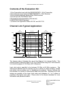
Channel link evaluation kit user manual national semiconductor corporation interface products lit# clink3v28bt-85-um rev 2.1 date: 10/12/2005 page 4 of 28 contents of the evaluation kit: 1) one transmitter board with the ds90cr287mtd - 28 bit transmitter 2) one receiver board with the ds90cr288amtd ...
Page 5: Power Connection:
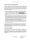
Channel link evaluation kit user manual national semiconductor corporation interface products lit# clink3v28bt-85-um rev 2.1 date: 10/12/2005 page 5 of 28 how to set up the evaluation kit: the pcb routing for the tx input pins (txin) have been laid out to accept incoming data from a 60-pin idc conne...
Page 6
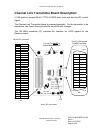
Channel link evaluation kit user manual national semiconductor corporation interface products lit# clink3v28bt-85-um rev 2.1 date: 10/12/2005 page 6 of 28 channel link transmitter board description: j1 (60 position) accepts 28 bit lvttl/lvcmos data, clock and also the pd* control signal. The channel...
Page 7
Channel link evaluation kit user manual national semiconductor corporation interface products lit# clink3v28bt-85-um rev 2.1 date: 10/12/2005 page 7 of 28 jumper settings for the tx board jumper purpose settings /pd powerdown = on = off (jp2) vcc gnd vcc gnd (on: tx is operational; off: tx powers do...
Page 8
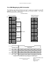
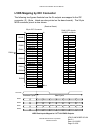
Channel link evaluation kit user manual national semiconductor corporation interface products lit# clink3v28bt-85-um rev 2.1 date: 10/12/2005 page 8 of 28 tx lvds mapping by idc connector the following two figures illustrate how the tx inputs are mapped to the idc connector (j1) (note – labels are a...
Page 9
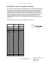
Channel link evaluation kit user manual national semiconductor corporation interface products lit# clink3v28bt-85-um rev 2.1 date: 10/12/2005 page 9 of 28 tx board options: 50 ohm termination for txin on the tx demo board, the 29 inputs have an option for 50 ohm terminations. There are 0402 pads for...
Page 10
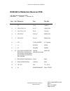
Channel link evaluation kit user manual national semiconductor corporation interface products lit# clink3v28bt-85-um rev 2.1 date: 10/12/2005 page 10 of 28 bom (bill of materials) transmitter pcb: hsl demo board schematic rev1 hsl8txr1 revision: 1 channel link item qty reference part pkg size 1 1 c1...
Page 11
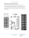
Channel link evaluation kit user manual national semiconductor corporation interface products lit# clink3v28bt-85-um rev 2.1 date: 10/12/2005 page 11 of 28 rx channel link receiver board: j1 (60 position) provides access to the 28 bit lvttl/lvcmos, clock outputs. The channel link receiver board is p...
Page 12
Channel link evaluation kit user manual national semiconductor corporation interface products lit# clink3v28bt-85-um rev 2.1 date: 10/12/2005 page 12 of 28 selectable jumper settings for the rx board jumper purpose settings /pd powerdown = on = off (jp1) vcc gnd vcc gnd (on: rx is operational; off: ...
Page 13
Channel link evaluation kit user manual national semiconductor corporation interface products lit# clink3v28bt-85-um rev 2.1 date: 10/12/2005 page 13 of 28 lvds mapping by idc connector the following two figures illustrate how the rx outputs are mapped to the idc connector (j1) (note – labels are al...
Page 14
Channel link evaluation kit user manual national semiconductor corporation interface products lit# clink3v28bt-85-um rev 2.1 date: 10/12/2005 page 14 of 28 rx optional: series termination for rxout on the rx demo board, there are 29 outputs that have an 0402 pad in series (which are shorted out). Th...
Page 15
Channel link evaluation kit user manual national semiconductor corporation interface products lit# clink3v28bt-85-um rev 2.1 date: 10/12/2005 page 15 of 28 bom (bill of materials) receiver pcb: hsl demo board schematic rev1 hsl8rxr1 revision: 1 channel link item qty reference part pkg size 1 1 c1 10...
Page 16
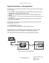
Channel link evaluation kit user manual national semiconductor corporation interface products lit# clink3v28bt-85-um rev 2.1 date: 10/12/2005 page 16 of 28 typical connection / test equipment the following is a list of typical test equipment that may be used to generate signals for the tx inputs: 1)...
Page 17: Typical Waveshapes
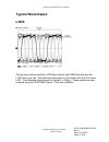
Channel link evaluation kit user manual national semiconductor corporation interface products lit# clink3v28bt-85-um rev 2.1 date: 10/12/2005 page 17 of 28 typical waveshapes lvds the plot above shows both the lvds data channel with prbs data and also the lvds clock over laid. Note that the clock pa...
Page 18: Rxout
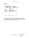
Channel link evaluation kit user manual national semiconductor corporation interface products lit# clink3v28bt-85-um rev 2.1 date: 10/12/2005 page 18 of 28 rxout the plot above shows both the recovered prbs data and also the regenerated clock overlaid. Note that the clock transitions slightly before...
Page 19: Troubleshooting
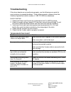
Channel link evaluation kit user manual national semiconductor corporation interface products lit# clink3v28bt-85-um rev 2.1 date: 10/12/2005 page 19 of 28 troubleshooting if the demo boards are not performing properly, use the following as a guide for quick solutions to potential problems. If the p...
Page 20: Additional Information
Channel link evaluation kit user manual national semiconductor corporation interface products lit# clink3v28bt-85-um rev 2.1 date: 10/12/2005 page 20 of 28 additional information for more information on channel link transmitters/receivers, refer to the national’s lvds website at: www.National.Com/ap...
Page 21: Appendix
Channel link evaluation kit user manual national semiconductor corporation interface products lit# clink3v28bt-85-um rev 2.1 date: 10/12/2005 page 21 of 28 appendix cable and connector the next few pages provide a full description of the cable and connector. For product request please contact 3m and...
Page 22
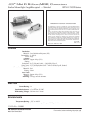
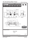
3m electronic products division 6801 river place blvd. Austin, tx 78726-9000 for technical, sales or ordering information call 800-225-5373 .050 ″ mini d ribbon (mdr) connectors surface mount right angle receptacle — shielded 102xx-1210ve series 140 important notice to purchaser all statements, tech...
Page 23
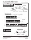
3m electronic products division 6801 river place blvd. Austin, tx 78726-9000 for technical, sales or ordering information call 800-225-5373 .050 ″ mini d ribbon (mdr) connectors surface mount right angle receptacle — shielded 102xx-1210ve series contact 3m part dimensions contact quantity 3m part nu...
Page 24
3m electronic products division 6801 river place blvd. Austin, tx 78726-9000 for technical, sales or ordering information call 800-225-5373 .050 ″ mini d ribbon (mdr) connectors surface mount right angle receptacle — shielded 102xx-1210ve series contact dimensions contact quantity a ± .002 b ± .002 ...
Page 25
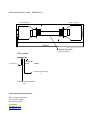
Cable assembly part number mdr26-5-6.5 3m mdr 10126-6000 3mmdr 10126-6000 2 meters spectra strip cable skew clear twin ax part number mdr26-5-6.5 cable length connector type 6.5 ft 2 meter number of twin-ax pairs 5 connector number of positions 26 cable assemby ordering information. Alliance technol...
Page 26
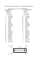
National semiconductor channel link cable assembley pinout alliance technology part number mdr26-5-6.5c pin assignment pin assignment side a side b 3m mdr part 3m mdr part 10126-6000 10126-6000 1 no connect 26 no connect 2 txout0gnd+ 25 txoutgnd- 3 no connect 24 no connect 4 txout1- 23 rxin1 - 5 txo...
Page 27
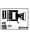
/pd +3.6v max +3.6v max hsl8tx hsl demo board schematic 1 1 monday, august 21, 2000 1 title size document number rev date: sheet of vcc1 lvds_vcc lvds_gnd vcc1 pll_vcc pll_gnd txin12 txin23 txin8 txin6 txin14 txin24 txin19 txin5 txin10 txin21 txin11 txin22 txin9 txin15 txin13 txin7 txin18 txin25 txo...
Page 28
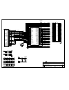
/pd +3.6v max +3.6v max hsl8rx hsl demo board schematic 1 1 monday, august 21, 2000 1 title size document number rev date: sheet of lvds_vcc pll_vcc vcc1 lvds_gnd vcc1 pll_gnd lvds_vcc pll_vcc pll_gnd pll_vcc pll_gnd lvds_vcc rxin3+ gnd1 rxin1+ rxclkin- rxin1- rxin0- lvds_gnd rxin0+ rxin3- gnd1 rxcl...


