National Semiconductor DS90C3202 Specifications

Manual is about: 3.3V 8 MHz to 135 MHz Dual FPD-Link Receiver

Summary of DS90C3202

  • Page 1

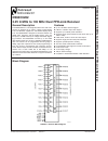
    Ds90c3202 3.3v 8 mhz to 135 mhz dual fpd-link receiver general description the ds90c3202 is a 3.3v single/dual fpd-link 10-bit color receiver is designed to be used in liquid crystal display tvs, lcd monitors, digital tvs, and plasma display panel tvs. The ds90c3202 is designed to interface between ...

  • Page 2

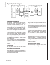
    Typical application diagram 20147102 figure 2. Lcd panel application diagram functional description the ds90c3201 and ds90c3202 are a dual 10-bit color transmitter and receiver fpd-link chipset designed to transmit data at clocks speeds from 8 to 135 mhz. Ds90c3201 and ds90c3202 are designed to inte...

  • Page 3

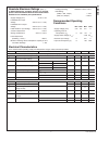
    Absolute maximum ratings (note 1) if military/aerospace specified devices are required, please contact the national semiconductor sales office/ distributors for availability and specifications. Supply voltage (v dd ) −0.3v to +4v lvcmos/lvttl input voltage −0.3v to (v dd + 0.3v) lvcmos/lvttl output ...

  • Page 4

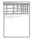
    Electrical characteristics (continued) over recommended operating supply and temperature ranges unless otherwise specified. Symbol parameter conditions min typ max units receiver supply current iccrw receiver supply current worst case (figures 2, 4) c l = 8 pf, worst case pattern default register se...

  • Page 5

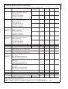
    Receiver switching characteristics over recommended operating supply and temperature ranges unless otherwise specified. Symbol parameter condition/ reference min typ max units clht lvcmos/lvttl low-to-high transition time, c l = 8pf, (figure 5) (note 8) register addr 28d/1ch, bit [2] (rclk)=0b (defa...

  • Page 6

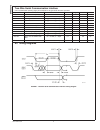
    Two-wire serial communication interface over recommended operating supply and temperature ranges unless otherwise specified. Symbol parameter conditions min typ max units f sc s2clk clock frequency 400 khz sc:low clock low period r p = 4.7k Ω, c l = 50pf 1.5 us sc:high clock high period r p = 4.7k Ω...

  • Page 7

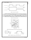
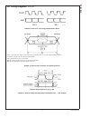
    Ac timing diagrams (continued) 20147103 figure 2. “worst case” test pattern 20147104 figure 3. Incremental test pattern 20147105 figure 4. Typical and max icc with worse case and incremental pattern 20147106 figure 5. Lvcmos/lvttl output load and transition times ds90c3202 www.National.Com 7.

  • Page 8

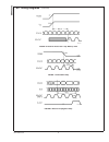
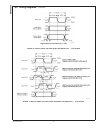
    Ac timing diagrams (continued) 20147107 figure 6. Receiver phase lock loop wake-up time 20147108 figure 7. Powerdown delay 20147109 figure 8. Receiver propagation delay ds90c3202 www.National.Com 8.

  • Page 9

    Ac timing diagrams (continued) 20147110 figure 9. Rfb: lvttl level programmable strobe select 20147111 ritol ≥ cable skew (type, length) + source clock jitter (cycle to cycle) (note 11) + isi (inter-symbol interference) (note 12) cable skew — typically 10 ps–40 ps per foot, media dependent please se...

  • Page 10

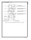
    Ac timing diagrams (continued) 20147113 registeraddress 29d/1dh bit [2:1] = 00b figure 12. Receiver rsrc and rhrc output setup/hold time — pto enabled 20147114 figure 13. Receiver rsrc and rhrc output setup/hold time adjustment — pto disabled ds90c3202 www.National.Com 10

  • Page 11

    Ac timing diagrams (continued) 20147115 figure 14. Receiver rsrc and rhrc output setup/hold time adjustment — pto enabled ds90c3202 www.National.Com 11.

  • Page 12

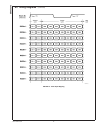
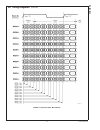
    Ac timing diagrams (continued) 20147116 figure 15. Lvds input mapping ds90c3202 www.National.Com 12.

  • Page 13

    Ac timing diagrams (continued) 20147117 figure 16. Receiver ritol min and max ds90c3202 www.National.Com 13.

  • Page 14

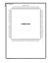
    Pin diagram ds90c3202 receiver 20147118 ds90c3202 www.National.Com 14.

  • Page 15

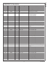
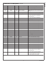
    Ds90c3202 pin descriptions pin no. Pin name i/o pin type description 1 s2dat i/op digital two-wire serial interface – data 2 s2clk i/p digital two-wire serial interface – clock 3 vddp1 vdd pll power supply for pll circuitry 4 vssp1 gnd pll ground pin for pll circuitry 5 vssp0 gnd pll ground pin for ...

  • Page 16

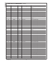
    Ds90c3202 pin descriptions (continued) pin no. Pin name i/o pin type description 46 vdd2 vdd lvttl o/p pwr power supply pin for lvttl outputs and digital circuitry 47 rxea0 o/p lvttl o/p lvttl level data output 48 rxea1 o/p lvttl o/p lvttl level data output 49 rxea2 o/p lvttl o/p lvttl level data ou...

  • Page 17

    Ds90c3202 pin descriptions (continued) pin no. Pin name i/o pin type description 92 rxoa4 o/p lvttl o/p lvttl level data output 93 rxoa5 o/p lvttl o/p lvttl level data output 94 rxoa6 o/p lvttl o/p lvttl level data output 95 vdd5 vdd lvttl o/p pwr power supply pin for lvttl outputs and digital circu...

  • Page 18

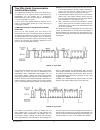
    Two-wire serial communication interface description the ds90c3202 operates as a slave on the serial bus, so the s2clk line is an input (no clock is generated by the ds90c3202) and the s2dat line is bi-directional. Ds90c3202 has a fixed 7bit slave address. The address is not user configurable in anyw...

  • Page 19

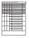
    Ds90c3202 two-wire serial interface register table address r/w reset bit # description default value 0d/0h r pwdn [7:0] vender id low byte[7:0] = 05h 0000_0101 1d/1h r pwdn [7:0] vender id high byte[15:8] =13h 0001_0011 2d/2h r pwdn [7:0] device id low byte[7:0] = 28h 0010_1000 3d/3h r pwdn [7:0] de...

  • Page 20

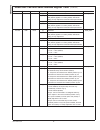
    Ds90c3202 two-wire serial interface register table (continued) address r/w reset bit # description default value 26d/1ah r/w none [7] reserved 0000_0000 [6:4] lvds input skew control for rxe channel b, 000 (default) applies to no delay added, one buffer delay per step adjustment towards thold improv...

  • Page 21

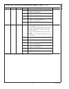
    Ds90c3202 two-wire serial interface register table (continued) address r/w reset bit # description default value 30d/1eh r/w none [7:5] reserved 0000_0000 [4] i/o disable control for rxe channel a, 1: disable, 0: enable (default) [3] i/o disable control for rxe channel b, 1: disable, 0: enable (defa...

  • Page 22

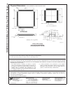
    Physical dimensions inches (millimeters) unless otherwise noted 128-pin tqfp package order number ds90c3202vs ns package number vjx128a national does not assume any responsibility for use of any circuitry described, no circuit patent licenses are implied and national reserves the right at any time w...