- DL manuals
- NEC
- Monitor
- Diamond Scan 51
- Service Manual
NEC Diamond Scan 51 Service Manual
Summary of Diamond Scan 51
Page 1
Models multisync v520 multisync v521 multisync mv521 diamond scan 51 color monitor (model no. N0501 series) service manual better service better reputation better profit /mitsubishi nec-mitsubishi electric visual systems.
Page 2
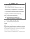
Product safety caution 1. When parts replacement is required for servicing, always use the manufacturer’s specified replacement. 2. Comply with all caution and safety-related notes on the product display chassis and picture tube. 3. When replacing the component, always be certain that all the compon...
Page 3: Contents
Contents page no. Precautions .................................................................................................................... 1 specifications ................................................................................................................ 3 pin adjustment table ...
Page 4
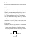
1 precautions follow these safety and servicing precautions to prevent damage and to protect against potential hazards such as electrical shock and x-rays. 1.1 safety precautions 1-1-1 warnings 1. For safety purpose, do not attempt to modify the circuit board, and always disconnect the ac power befo...
Page 5
C) reverse the ac plug at the ac outlet and repeat the steps for ac voltage measurements for each exposed metal part. D) voltage reading must not exceed 0.3 volts rms, equivalent to 0.2 milliampere ac. Any value ex- ceeding this limits ill constitute a potential shock hazard and must be corrected im...
Page 6
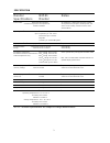
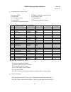
Specification note: technical specifications are subject to change without notice. Monitor specifications n0501 monitor notes picture tube diagonal: viewable image size: radius: 38cm(15inch) 35cm(13.8inch) 1080mm 90° deflection, 0.28mm trio dot pitch, medium short persistence phosphor, multi-layered...
Page 7
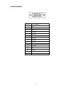
Pin assignment 1 2 3 4 5 6 7 8 9 10 11 12 13 14 15 pin no. Mini d-sub-15p 1 red 2 green 3 blue 4 ground 5 ground 6 ground 7 ground 8 ground 9 no pin 10 ground 11 ground 12 sda 13 h.Sync. 14 v.Sync. 15 scl 4.
Page 8
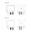
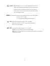
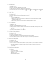
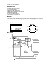
Controls ”select”: to display osm windows, mode changes, or activate the degaussing or osm window color selection. Control button (-,+): without osm — adjust the contrast. With osm — select icon and adjust. ”reset”: return the adjustment item to the factory setting. Power indicator led: the led indi...
Page 9
6 multisync mv521 diamand scan 51.
Page 10
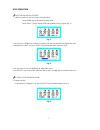
Osd operation „p „p „p „p „p function value adjustment if osd off, press up key to increase contrast value, press down key to decrease contrast value. Press select key to display osd and brightness icon is active (fig. 1) fig. 1 press up key or down key to select icon right or left and the selected ...
Page 11
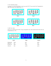
2. Color temperature select if selected icon is 9300/7500/6500/user color icon, press select key to select color temperature for 9300, 7500, 6500 or user defined (fig 4 – 7). 3. Osd color select if osd icon is selected, press select key to change osd color, there are three kinds of osd color can be ...
Page 12
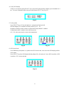
4. Sync osd display if exit icon is selected, press select key to close osd menu and then display sync information for 2 sec. This sync information will not be close until release select key (fig. 11). 5. Factory mode press select key + up key and power on, system enter factory mode. Osd will displa...
Page 13
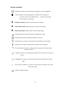
Function explanation brightness: adjusts the overall image and background screen brightness. Contrast: adjusts the image brightness in relation to the background. (contrast control is also effective with “-, +” button even through osm window is not existing.) r red color control: adjust the red cont...
Page 14
Degauss: select the degauss icon on “icon select window” and push “select” button. It will eliminate the stray magnetic field and correct the scan the electron beam, and will affect the purity, focus, convergence. Caution: allow a minimum interval of 20 minutes to elapse between uses of the degauss ...
Page 15: 0 0
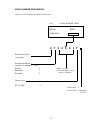
Serial number information refer to the serial number information shown below. Ex.) serial number label model n0501 serial no. ∗∗∗∗∗∗∗∗∗ 0 y 1 y 0 0 0 0 00001 ~ on ward (start from 00001 ~ when month is changed.) manufactured year : ( last digit ) manufactured month : january to september 1 to 9 octo...
Page 16
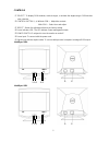
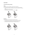
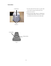
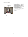
Disassembly tilt / swivel base fixing, removing fixing this product consists of the multisync monitor and the tilt / swivel base. When fixing the tilt / swivel base to the multisync monitor, please follow the steps below. • push the six hooks of the tilt / swivel base into the six holes at the botto...
Page 17
Cabinet back 1.Turn the monitor crt face down on a clean static free surface to prevent scratching crt face. 2.Remove the screw “b”. 3.Raise the signal cable vicinity of a cabinet back and lightly hit part (figure 1 reference) of a top of the cabinet back and remove the cabinet back. Cabinet back sc...
Page 18
Main board and crt board 1. Unsolder the gnd wire from main board assy 2. Disconnect the connector “p201”, “p202”, “s204” and “s205” from the crt board assy. 3. Disconnect the crt board assy from the crt 4. Disconnect the connector “s301” and “p102” from the main board assy. 5. Remove the anode cap ...
Page 19
Adjustment specifications table of contents page (1) adjustment & inspection tools .......................................................................................................... 17 (2) timing table .............................................................................................
Page 20
N0501 adjustment specifications ver. 1.1 2000,11,16 (1) adjustment & inspection tools: (a) color analyzer (b) signal generator charoma 2135 (c) multi meter (d) hi-voltage probe (e) convergence meter (f) demagnetizer (g) power meter (h) automatic alignment system (i) ddc write & inspection system (2)...
Page 21
(5) b+ adjustment (a) mode: no. 12. (b) pattern: full white. (brightness just cut off) (c) adjust vr101 to make the cathode of d112 has 13.6v. (d) check other power source should be 78 ¡Ó ¡Ó ¡Ó ¡Ó ¡Ó 2v, 6.2v ¡Ó ¡Ó ¡Ó ¡Ó ¡Ó 0.3v, 53.5v ¡Ó ¡Ó ¡Ó ¡Ó ¡Ó 1.5v, -11.5 ¡Ó ¡Ó ¡Ó ¡Ó ¡Ó 0.5v. (6) x-ray test (...
Page 22
(b) cut off adjustment 1. Select the color mode 9300k 2. Cut off adjustment: video signal off (0.Vp-p), bright control set to mex., adjust the screen vr(g2), at the brightness 1~1.5fl. (3.4~5.1 cd/m2) 3. Adjust vr210, vr230 and vr250 to make x=283, y=297, with readjusting g2 to keep the brightness b...
Page 23
(13) power saving function inspection (a) mode: no. 12 (b) pattern: any pattern (c) inspection 1. It should be into power off mode when the both horizontal sync and vertical sync are disable after 4 seconds. Check the led color “orange” and the power consumption must be less then 5w. 2. The picture ...
Page 24
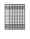
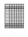
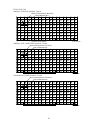
(18) timing sheet for n0501/n0701 p re s e t m o d e n o . 1 2 3 4 5 6 s ig n a l n a m e v g a 3 5 0 v g a 4 0 0 v g a 4 8 0 m a c ii 8 0 0 * 6 0 0 8 5 1 4 /a (3 5 k ) (5 6 ) x g a r e s o lu tio n 6 4 0 * 3 5 0 6 4 0 * 4 0 0 6 4 0 * 4 8 0 6 4 0 * 4 8 0 8 0 0 * 6 0 0 1 0 2 4 * 7 6 8 d o t c lo c k ...
Page 25
P re s e t m o d e n o . 7 8 9 1 0 11 1 2 s ig n a l n a m e 6 4 0 * 4 8 0 e v g a 4 0 0 8 0 0 * 6 0 0 6 4 0 * 4 8 0 8 0 0 * 6 0 0 1 0 * 7 (6 0 ) (7 5 ) (v e s a ) (6 0 ) (8 5 ) (7 5 ) (v e s a ) r e s o lu tio n 6 4 0 * 4 8 0 6 4 0 * 4 0 0 8 0 0 * 6 0 0 6 4 0 * 4 8 0 8 0 0 * 6 0 0 1 0 2 4 * 7 6 8 d...
Page 26
P re s e t m o d e n o . 1 3 1 4 1 5 1 6 17 1 8 s ig n a l n a m e m a c ii 8 0 0 * 6 0 0 1 0 * 7 (7 0 ) 1 0 * 7 (7 5 ) 640*480 1 2 * 1 0 (6 0 ) (4 9 .7 k ) (8 5 ) (v e s a ) (v e s a ) (120) (v e s a ) r e s o lu tio n 8 3 2 * 6 2 4 8 0 0 * 6 0 0 1 0 2 4 * 7 6 8 1 0 2 4 * 7 6 8 640*480 1 2 8 0 * 1 ...
Page 27
P re s e t m o d e n o . 19 2 0 s ig n a l n a m e 800*600 1 0 2 4 * 7 6 8 (100) (8 5 ) r e s o lu tio n 800*600 1 0 2 4 * 7 6 8 d o t c lo c k (m h z ) 67.50 9 4 .5 fh (k h z ) 63.92 6 8 .6 7 7 fv (h z ) 100.03 8 5 to ta l (d o t) 1056 1 3 7 6 (u s ) 15.64 1 4 .5 6 1 d is p (d o t) 800 1 0 2 4 (u s...
Page 28
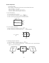
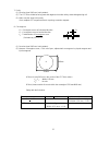
Distortion adjustment factory mode setting *after completion of adjustment exit the factory mode and data will be saved. Signal : all signals cross hatch perform the adjust for signal no. 14 in step 6-1~3. Perform the adjust for above all signal in step 6-4,5. 1. Picture tilt adjustment (1) receive ...
Page 29
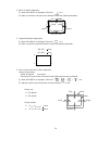
4. Side pincushion adjustment (1) when osm menu is displayed, select the “ “ icon. (2) make sure that the side pincushion distortion meets the following standards. 1.5mm 1.8mm 1.5mm 1.8mm 1.8mm 1.8mm 1.8mm 1.8mm 5. Trapezoid distortion adjustment (1) when osm menu is displayed, select the “ “ icon. ...
Page 30
A b 270mm 203mm a zone (a circle 203 mm in the center of the crt face center) c h , c v : within 0.35 mm c s : no rule b zone (areas outside of zone a within the rectangle of 270 mm × 203 mm) safety with the list below. C h 0 .3 5 m m h c v o k c a lc u la te c s a n d ju d g e w ith in 0 .5 0 m m →...
Page 31
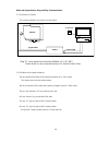
Write and inspection for plug and play communication 1. C onstruction of system this system should be connected as shown below. Monitor program disk pc signal cable fixture power cable note: pc clock speed should be below 266mhz. Os is pc-dos. Fixture board can be connected directly to pc without pr...
Page 32
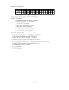
0 1 2 3 4 5 6 7 8 9 a b c d e f 00 00 ff ff ff ff ff ff 00 38 a3 1d 25 01 01 01 01 10 18 09 01 02 0c 1c 15 78 ea b4 18 a1 55 48 99 25 20 10 48 4c ff ee 00 31 59 45 59 61 59 71 4a 81 40 30 01 01 01 01 01 01 30 2a 00 98 51 00 2a 40 30 70 40 13 00 0e cb 10 00 00 1e 00 00 00 fd 00 37 78 1f 50 46 0b 00 0...
Page 33
*+set assembly code + 1 space + serial no. + * set assembly code depends on the crt and destination. Serial no. Descriptions: y: manufactured year (last digit) ex. 0 à 2000 m: manufactured month 1 ~ 9, x(october), y(novenber), z(december) s: serial no. ( 5digits) 00001 ~ onward (restart when month i...
Page 34
Trouble shooting refer to user’s manual trouble shooting section before using this chart. Table of contents page 1. No operation, power led flash ....................................................................................... 32 2. No operation, power led off ...................................
Page 35
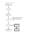
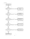
1. No operation, power led flash 1. Dc p/s o/p voltage set at 17v,current set at 600ma. Positive connect to c130”+”. Negative connect to u102-pin 5. 2. Scope set at 10v/div, 10us/div, probe connect to q102-gate and u102pin 5. Power led flash check u102 u102 pin6 pulse o/p power sw turn off failure r...
Page 36
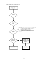
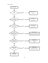
2. No operation, power led off 1. Dc p/s o/p voltage set at 17v,current set at 200ma. Positive connect to c112”+”. Negative connect to c105”-“. 2. Scope set at 10v/div, 10us/div, probe connect to q101-gate and c105”-“. Power sw turn off check f101 check q101 check u101 u101 pin6 pulse o/p power sw t...
Page 37
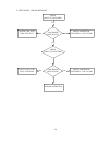
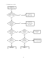
3. Video noise, unsynchronous check horizontal frequency c114 to gnd check q101 g-s frequency syncronize with h-sync check horizontal frequency c132 to gnd check c132, r139, d115, r138, r140 normal operation check q101 g-s frequency syncronize with h-sync check c114, r116 d109, r115, r117 yes yes no...
Page 38
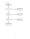
4. No video no video yes check screen control clockwise yes check u201 pin 5, 8, 11 signal level yes check u201 pin 18, 20, 23 signal level trouble in u201 clamp(pin 15) u201 12v voltage yes check u203 pin 1, 2, 3 signal level check cathode video level problem in crt yes yes trouble in u203 r220, r2...
Page 39
5. No raster check u301 pin 3, u402 pin 4 h/v sync no raster power supply check check b+ check u301 pin 7, u402 pin 23,24 h/v sync check t301 pin 3 voltage 68v(at h-freq. 31.5khz) trouble in mcu u701 trouble in u301, u402 trouble in u102,q102,d114,d111,l102 or deflection yoke trouble in q307, q308,t...
Page 40
6. Trouble in h. V sync trouble in hor. Or ver. Sync check connector s702 (pin3,4), signal trouble in signal cable check u701(pin 40,39) h/v sync. Signal trouble in h/v sync line & q301, q401 check u701(pin 32,33) h/v sync. Signal check u701(pin 5) voltage 5v? Check u301(pin 3) u402(pin 4) check u70...
Page 41
7. Pincushion poor pincushion poor parabola wave check u402 pin 9 parabola check u401 pin 4 sync input check u701 (pin 32) output check c431, r432 check 12v & u402 check q314~q316, d308 no no no yes yes yes 38.
Page 42
Circuit description table of contents page 1. Power supply circuit ................................................................................................................. 40 2. Mcu ................................................................................................................
Page 43
1. Power supply circuit outline this power supply unit adopts the switching mode technology, and is an off-line mode type unit that provided several different dc outputs. The scanning frequency is available in different values ranging from 31 khz to 69 khz. Moreover, it is capable to operate at an a...
Page 44
2) the power supply mos fet q101 carries out the on/off operation of the control unit, by means of u101 ka3842a. Ka3842a is a pwm (pulse width modulation) ic chip, with 16 v starting voltage and 10 v cut-off voltage. The following list shows the pin layout of ka3842a pulse width modulation ic chip. ...
Page 45
Dc/dc the dc/dc voltage is dc 45 volts, and since the set-up voltage is variable from 60 volts to 160 volts, it is variable depending on the horizontal synchronism. The frequency band is variable from 31 khz to 65 khz. The voltage is fed back from the fly-back transformer (fbt). The dc/dc output vol...
Page 46
2. Mcu monitor mcu specification frequency specification h-freq. : 29.5k – 70khz v-freq. : 43 – 160hz judge polarity only when frequency is 31.5 khz and 37.8 khz support composite sync detection system architecture 1. Mcu – weltrend wt6016, 16k bytes rom size 2. Eeprom – 24c04 series, 4k bit, with i...
Page 47
3.Power saving – 2 pins (pmus, pmuo) for power saving control – if hf > 70khz or hf 23khz, enter power saving mode (suspend). – enter power saving mode after 3 sec when condition met. – enter suspend mode first for 3 sec before enter off mode if off mode condition met. Mode h-sync freq. V-sync freq....
Page 48
Iic interface 1. Ddc1/ddc2b – vesa ddc1/ddc2b is supported. 2. Auto alignment – i²c auto alignment protocol is supported. Timing table total 24 modes. 1. Factory mode – 20 modes mode resolution h-sync. V-sync. H polarity v polarity 1 vga 350 31.5khz 70hz + - 2 vga 400 31.5khz 70hz - + 3 vga 480 31.5...
Page 49
Pin definition pin name description i/o 1 da2 pin-balance pwm o 2 da1 h position pwm o 3 da0 h size pwm o 4 reset low reset i 5 vdd +5v i 6 vss ground i 7 osc o 8mhz crystal out o 8 osc i crystal in i 9 pb5 eeprom/osd sda i/o 10 pb4 eeprom/osd scl o 11 pb3 test pattern o 12 pb2 cs1 o 13 pb1 cs0 o 14...
Page 50
General description the wt6016 is a member of wt60xx microcontroller family. It is specially designed for digital con- trolled multi-sync monitor. It contains 8-bit cpu, 16k bytes rom, 288 bytes ram, 14 pwms, parallel i/ o, sync processor, timer, one ddc interface (slave mode i²c interface with ddc1...
Page 51
Pin description pin no. 40 42 pin name i/o descriptions 1 1 da2 o d/a converter 2. Open-drain output. External applied voltage can up to 10v. 2 2 da1 o d/a converter 1. Open-drain output. External applied voltage can up to 10v. 3 3 da0 o d/a converter 0. Open-drain output. External applied voltage c...
Page 52
Sync processor the sync processor can : (1) separate the composite sync signal; (2) calculate hsync and vsync frequencies; (3) detect polarities of hsync and vsync input; (4) control the output polarities of hso and vso pin; (5) generate free-running horizontal and vertical sync signals for burn-in ...
Page 53
Frequency calculation horizontal frequency and vertical frequencies calculation are done by using one 10-bit up counter. After power is on, the sync processor calculates the vertical frequency first (h/v bit = ”0”). A 31.25khz clock counts the time interval between two vsync pulses, then sets the fr...
Page 54
Test pattern generation a self-test pattern signal comes out from pin pb3/pat. It can generate a cross hatch picture, a inverted cross hatch picture, a whit epicture or a black picture. 8 × 8 cross hatch inverted 8 × 8 cross hatch white picture black picture the test pattern signal is generated when...
Page 55
Ddc interface the ddc interface is a slave mode i ² c interface with ddc1 function. It is fully compatible with vesa ddc1/2b standard. The functional block diagram is shown in the below. Data buffer shift register address compare 1 address register 0 1 0 0 0 0 mux mux enack addr r/w vsync msb intern...
Page 56
If a low level occurs on the scl pin in ddc state, the ddc interface will switch to ddc2b state immediately and set the ddc2b bit to “1”. No interrupt will be generated. But, if there is no valid device address and it receives 128 vsync pulses while the scl is high level, it will lock into ddc2b sta...
Page 57
(5) data bytes transmit/receive if the rw bit is “1”, the shift register will load data from the data buffer (reg#18h) before the data byte is transmitted and shift out data to the sda pin before the rising edge of the scl clock. If the rw bit is “0”, the shift register will shift in data on the ris...
Page 58
Pull low scl pull low scl pull low scl data byte data byte scl 1 1 0 0 0 0 0 0 a a a sda in sda out into write reg#19h to release shift register to data buffer ddc2b=1 addr=0 r/w=0 start=0 stop=1 ddc2b=1 addr=0 r/w=0 start=0 stop=0 ddc2b=1 addr=0 r/w=0 start=0 stop=0 ddc2b=1 addr=0 r/w=0 start=1 sto...
Page 59
3. 2-wire serial cmos e ² ropm outstanding features § internally organized 512 × 8 (4k) § two-wire serial interface § bidirectional data transfer protocol § write protect pin for hardware data protection § 16-byte page write modes § partial page writes are allowed § self-timed write cycle (10 ms max...
Page 60
4. Horizontal deflection signal processing lm1290: 1. Full-automatic synchronization from 22 khz to 90 khz. No component changeover nor external adjustment is required. 2. Dc control h phase and duty cycle. 3. The resistance corresponds to the frequency programmable down to vco. 4. X-ray input inval...
Page 61
1. Pin 1. Fmin: lower limit frequency of this setting. Fmin = 5.6 × 10 8 / (rmin*500) fmin = 29.1 khz, rmin = 18.7k Ω (when the frequency is 30khz or more) fmin = 22.8 khz, rmin =24k Ω (when the frequency is 24khz or more) 2. Pin 2. Polarity of h/hv: c pol = 0.1uf, io = ± 1ua , vo = 1-e-t/rc 3. H/hv...
Page 62
5. Vertical compensation and geometrical compensation of the raster lm1295: 1. Vertical scanning frequency : 50 to 100hz. 2. Dc control compensation amplitude 3. Temperature stability of the vertical amplitude : 1%. 4. Dynamic vertical deflection compensation corresponding to the secondary anode vol...
Page 63
1. V-height (pin-2): the amplitudes of the +v and –v drive currents are controlled by means of the 0v to 4v voltage of this pin. The current can be raised by raising by raising the voltage. The control range is approximately 1.8 to 1. 2. 4v cap (pin 3): 4 v cap (capacitor), 10 uf capacitor. 3. V-syn...
Page 64
11. Output of the parabola and bow-shaped parabola (pin 14): the amplitude and the polarity of the ramp signal are controlled by means of the para cntrl (pin 12), and the amplitude and polarity of the parabola are controlled by the bow cntrl (pin 13). In both cases, the control is carried out in the...
Page 65
6. Full bridge current driver vertical deflection booster tda4866 1. Fully built-in type construction, with practically no external component. 2. High-grade amplification of the linear sawtooth wave signal. 3. High-efficiency dc coupling vertical bridge circuit. 4. Powerless vertical shift 5. Deflec...
Page 66
7. Horizontal drive and power supply output circuit diagram description of the circuit: 1) r1, t1 and q2 compose the horizontal driving circuit, and the transistor q1 generates a horizontal output through the driving signal. Ib1 = i cpmax / q1h femin i b2 ¡Ü ¡Ü ¡Ü ¡Ü ¡Ü 3i b1 di/dt ¡Ü ¡Ü ¡Ü ¡Ü ¡Ü 3....
Page 67
8. Horizontal amplitude control circuit diagram description of the circuit: 1) the diodes d1 and d2 compose the bipolar modulation circuit, and have the function of controlling the currents of the oils dy(lpp) and lm(lm) through voltage modulation carried out by utilizing vm. B+ = vm +vcs therefore,...
Page 68
9. Fly-back line erasing unit & spot erasing unit circuit diagram description of the circuit: 1) the vertical blanking circuit completes by q1, q2, q3 and peripheral circuit. The vertical sync pulse applied to r3, r12 connected to q5 base. Q5 is invert amplifier, then mixer with q1 base together for...
Page 69
10. Video amplifier system with on-screen display lm1281 (u201) outstanding features: * three-channel video amplifier bandwidth 85 mhz @ -3 db (4 vp-p output) * osd ttl input, bandwidth 50 mhz * high-speed video/osd changeover * high impedance dc contrast control above the 0-4v, 40db range * high im...
Page 70
Test circuits figure 2 lm1281 osd video preamp demonstration board schematic red osd input green osd input blue osd input osd input select red video in green video in blue video in video contrast red drive adj. Green drive adj. Blue drive adj. Rgb cutoff adj. Red video out** green video out** blue v...
Page 71
11. Monolithic triple 13.5ns crt driver 68.
Page 72
69.
Page 73
70
Page 74
71.
Page 75
12. On screen display features • horizontal sync input may be up to 100 khz. • on-chip pll circuitry up to 90mhz pixel rate for multi-sync operation. • programmable horizontal resolutions up to 1524 dots per display row. • 538 bytes display registers to control full screen display. • full screen dis...
Page 76
1.0 connection diagram (16 pins pdip 300 mil package) 2.0 pin descriptions 1 2 3 4 5 6 7 8 9 10 11 12 13 14 15 16 mtv016-n vssa vco rp vdda hflb ssb sda sck vss rout gout bout fbkg htone vflb vdd name i/o pin# function vssa - 1 analog ground. This ground pin is used to internal analog circuitry. Vco...
Page 77
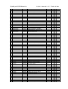
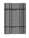
Replacement parts list 1) multisync v520 parts list b: asia, c: china, r: australia, t: toshiba, l: lg, o: orion 74 assy code part no description location q'ty alt remark 1 cabinet front assy 10100552 cabinet front 1 2 cabinet front assy 11300351 push buttom(a)-fuction key 1 3 cabinet front assy 113...
Page 78
75 53 crt board a/i ej044148 diode "t" 1n4148 d204 1 54 crt board a/i ej044148 diode "t" 1n4148 d205 1 55 crt board a/i ej044148 diode "t" 1n4148 d210 1 56 crt board a/i ej044148 diode "t" 1n4148 d211 1 57 crt board a/i 80000451 diode/t 1/2w 1ss83 d212 1 58 crt board a/i 80000051 diode/t 1/2w 1ss82 ...
Page 79
76 106 crt board a/i r0319110 jumper wire ai/t 15mm j27 1 107 crt board a/i r0319110 jumper wire ai/t 7.5mm j28 1 108 crt board a/i r0319110 jumper wire ai/t 7.5mm j29 1 109 crt board a/i r0319110 jumper wire ai/t 7.5mm j3 1 110 crt board a/i r0319110 jumper wire ai/t 7.5mm j30 1 111 crt board a/i r...
Page 80
77 159 crt board a/i fa040221 carbon 1/8w(t) 5% 220ohm r270 1 160 crt board a/i fa240223 carbon 1/4w(t) 5% 22kohm r278 1 161 crt board a/i fa240223 carbon 1/4w(t) 5% 22kohm r280 1 162 crt board a/i fa040472 carbon 1/8w(t) 5% 4.7kohm r282 1 163 crt board a/i fa040112 carbon 1/8w(t) 5% 1.1kohm r284 1 ...
Page 81
78 212 main board a/i ga322645 elect 85oc/t 22u/35v m c109 1 213 main board a/i gb747153 ceramic y5p(b)/t 470p/50v k c110 1 214 main board a/i ge210352 plastic pei/t 0.01u/50v j c111 1 215 main board a/i gb910358 ceramic z5v(f)/t 0.01u/50v z c112 1 216 main board a/i ga310655 elect 85oc/t 10u/50v m ...
Page 82
79 265 main board a/i gf210262 mef cap box 0.001u/63v j c315 or 266 main board a/i gf247262 mef cap box 0.0047u/63v j c316 1 267 main board a/i gf247252 mef cap box 0.0047u/50v j c316 or 268 main board a/i ga347455 elect 85oc/t 0.47u/50v m c317 1 269 main board a/i ga322725 elect 85oc/t 220u/16v m c...
Page 83
80 318 main board a/i gf210462 mef cap box 0.1u/63v j c448 1 319 main board a/i gf210452 mef cap box 0.1u/50v j c448 or 320 main board a/i ga347555 elect 85oc/t 4.7u/50v m c450 1 321 main board a/i ge268252 plastic pei/t 0.0068u/50v j c601 1 322 main board a/i ge210352 plastic pei/t 0.01u/50v j c603...
Page 84
81 371 main board a/i ejac0018 diode/t 1a 1n4937 d322 1 372 main board a/i ej044148 diode "t" 1n4148 d323 1 373 main board a/i ejac0018 diode/t 1a 1n4937 d324 1 374 main board a/i ej044148 diode "t" 1n4148 d325 1 375 main board a/i ejac0018 diode/t 1a 1n4937 d328 1 376 main board a/i ejac0018 diode/...
Page 85
82 424 main board a/i r0319110 jumper wire ai/t 15mm j133 1 425 main board a/i r0319110 jumper wire ai/t 15mm j134 1 426 main board a/i r0319110 jumper wire ai/t 17.5mm j135 1 427 main board a/i r0319110 jumper wire ai/t 17.5mm j136 1 428 main board a/i r0319110 jumper wire ai/t 17.5mm j137 1 429 ma...
Page 86
83 477 main board a/i r0319110 jumper wire ai/t 12.5mm j61 1 478 main board a/i r0319110 jumper wire ai/t 7.5mm j62 1 479 main board a/i r0319110 jumper wire ai/t 20mm j64 1 480 main board a/i r0319110 jumper wire ai/t 10mm j66 1 481 main board a/i r0319110 jumper wire ai/t 10mm j67 1 482 main board...
Page 87
84 530 main board a/i eaa09456 tr npn 2sc945p to-92(t) (n.P.S.) q107 or 531 main board a/i eba09281 tr pnp ksa 928a to-92(t) (samsung) q108 1 532 main board a/i eba10205 tr pnp 2sa1020y to-92(t) q108 or 533 main board a/i eaa18157 tr npn 2sc1815gr to-92(t) (t.P.S.) q110 1 534 main board a/i eaa09456...
Page 88
85 583 main board a/i fa040752 carbon 1/8w(t) 5% 7.5kohm r113 1 584 main board a/i fa330104 carbon 1/2w(t) 5% 100kohm r114 1 585 main board a/i fa040390 carbon 1/8w(t) 5% 39ohm r115 1 586 main board a/i fa240271 carbon 1/4w(t) 5% 270ohm r116 1 587 main board a/i fa240390 carbon 1/4w(t) 1% 39ohm r117...
Page 89
86 636 main board a/i fa330561 carbon 1/2w(t) 5% 560ohm r308 1 637 main board a/i fa040224 carbon 1/8w(t) 5% 220kohm r30c 1 638 main board a/i fa040224 carbon 1/8w(t) 5% 220kohm r30e 1 639 main board a/i fa040103 carbon 1/8w(t) 5% 10kohm r310 1 640 main board a/i fb910010 metal 1/4w(t) 5% 1ohm r313 ...
Page 90
87 689 main board a/i fa040472 carbon 1/8w(t) 5% 4.7kohm r383 1 690 main board a/i fa330150 carbon 1/2w(t) 5% 15ohm r385 1 691 main board a/i fb241002 metal 1/4w(t) 1% 10kohm r386 1 692 main board a/i fa040132 carbon 1/8w(t) 5% 1.3kohm r387 1 693 main board a/i fa040153 carbon 1/8w(t) 5% 15kohm r390...
Page 91
88 742 main board a/i fa240222 carbon 1/4w(t) 5% 2.2kohm r609 1 743 main board a/i fa040472 carbon 1/8w(t) 5% 4.7kohm r610 1 744 main board a/i fa040223 carbon 1/8w(t) 5% 22kohm r611 1 745 main board a/i fa040103 carbon 1/8w(t) 5% 10kohm r612 1 746 main board a/i fa040103 carbon 1/8w(t) 5% 10kohm r6...
Page 92
89 795 main board a/i ekc00507 zen diode 1/2w(t) bzx79f5v1 (philips) zd701 or 796 main board a/i eka00507 zen diode 1/2w(t) hzs5c2 (hitachi) zd702 1 797 main board a/i ekc00507 zen diode 1/2w(t) bzx79f5v1 (philips) zd702 or 798 main board a/i eka00507 zen diode 1/2w(t) hzs5c2 (hitachi) zd703 1 799 m...
Page 93
90 848 main board insert 80003551 diode 200v/1.6a rg2z sanken Ås¨¤ d118 849 main board insert 14000041 screw (p-#2cbrits*3*8*15bf) d307 1 850 main board insert 80001171 diode/a 5tuz47c (toshiba) d307 1 851 main board insert 80009541 diode fagor fuf5406 Ås¸} (a+k) d308 1 852 main board insert 8000113...
Page 94
91 901 main board insert fb560152 mof 2w/m(a) 5% 1.5kohm r134 1 902 main board insert fc030338 wound res 1w/m(a) 5% 0.33ohm r136 1 903 main board insert fb470623 mof 1w/m(a) 5% 62kohm r143 1 904 main board insert 80002031 fuseable res 1/2w(a)m 0.22 ohm r150 1 905 main board insert 80002031 fuseable ...
Page 95
92 954 main board insert 80010021 n9701 ve wire assy wire assy 1 955 main board insert em08003 x'tal 49u 8mhz x701 1 956 main board insert 18000321 edge saddle(sb-31) 1 957 main board insert 80010741 gnd wire black 180mm 18awg 1015 4.3d 1 958 packing assy 11000381 revolving assy 2 nd tooling or 959 ...
Page 96
93 1007 set assy r0191207 tape black l=75mmx3 tape 0.015 1008 set assy 17000321 cable ties(gt-100m) tie 9 1009 set assy 10100542 cabinet front assy 1 1010 set assy 10100563 cabinet back 1 1011 set assy 12300202 plate shielding (video) 1 1012 set assy 15000881 name plate insertuction v520-1(b ver.) 1...
Page 97
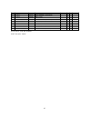
2) multisync v521 different list b: asia, r: australia, l: lg, t:toshiba, s:samsung 94 assy code part no description location q'ty alt remark 1 cabinet front assy 10101111 cabinet front(pc+abs) 1 2 cabinet front assy 11300351 push button (control a) 1 3 cabinet front assy 11300781 push button (sw) 1...
Page 98
95 54 set assy 80000891 wire l=360mm black awg18 gnd wire 1 55 set assy 80001931 17" rotation coil gnd wire 1 56 set assy 80010951 ms75 crt gnd wire gnd wire 1 57 set assy 72000641 tco pcb pcb tco 1 58 set assy 80005101 wire 1618 24awg 40mm bk shield wire 1 59 set assy r0191207 tape black l=75mmx3 t...
Page 99
96 3) multisync mv521 different list assy code part no description location q'ty alt remark 1 cabinet front assy 10101032 cabinet front(pc+abs) 1 2 cabinet front assy 11300351 push buttom(v)-fuction key 1 3 cabinet front assy 11300781 push buttom(sw)-power knob 1 4 cabinet front assy 11600121 lens(v...
Page 100
54 set assy 15200331 lable serial barcode(b ver.) 1 55 set assy 15200471 lable warning (27.5kv/600ua) 1 56 set assy 15200681 label tco99 1 b 57 set assy 15201061 label safety(russia+poland for cabinet) 1 58 set assy 17000252 copper sheilding(v500pnr) 1 59 set assy 18000331 wire clip (wc-13t) 1 60 se...
Page 101
4) diamond scan 51 different list assy code part no description location q'ty alt remark 1 cabinet front assy 10100721 cabinet front 1 2 cabinet front assy 11300481 push button(function) 1 3 cabinet front assy 11300491 push button(sw) 1 4 cabinet front assy 11600181 lens 1 5 cabinet front assy 13000...
Page 102: N0501(V520/v521/mv521/ds51)
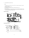
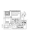
N0501(v520/v521/mv521/ds51) s m p s horizontal and vertical sync processor lm1290+lm1295 h v ew-out & hout / v.Geometry system architecture mcu/e²rom/ddc wt6016+24c04 mother board key-board i²c hor deflect-stage b+ ka3843 dynamic focusing vert out tda 4866 eh.T. D.F r g b fblk osd mtv-016 rgb preamp...
Page 103
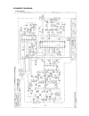
95 schematic diagrams 1) video board.
Page 104
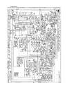
96 2) main board.


