- DL manuals
- NEC
- Monitor
- LCD1501-BK
- Service Manual
NEC LCD1501-BK Service Manual
Summary of LCD1501-BK
Page 1
Color monitor lcd1501 model lcd1501-bk(b) 200211 08r390b3 service manual part no. 599910613 nec-mitsubishi electric visual systems corporation november 2002.
Page 2
Warning the service personnel should have the appropriate technical training, knowledge and experience necessary to: • be familiar with specialized test equipment, and • be careful to follow all safety procedures to minimize danger to themselves and their coworkers. To avoid electrical shocks, this ...
Page 3: Contents
Contents page no. User's manual ------------------------------------------------------------------- 1-1 serial number information --------------------------------------------- 2-1 disassembly ----------------------------------------------------------------------- 3-1 adjustment procedures ----------...
Page 4: User'S Manual
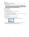
1-1 user's manual lcd1501 user’s manual uÏivatelská pfiíruãka bedienerhandbuch Οδηγίες Χρήσης manual del usuario manuel utilisateur manuale utente gebruikershandleiding podr´cznik u˝ytkownika Руководство пользователя kullan∂c∂ klavuzu.
Page 5
1-2 for the customer to use in u.S.A. Or canada canadian department of communications compliance statement doc: this class b digital apparatus meets all requirements of the canadian interference-causing equipment regulations. Cet appareil numérique de la classe b respecte toutes les exigences du règ...
Page 6
1-3 congratulations! You have just purchased a tco’99 approved and labeled product! Your choice has provided you with a product developed for professional use. Your purchase has also contributed to reducing the burden on the environment and also to the further development of environmentally adapted ...
Page 7
1-4 index warning, caution ............................... English-1 declaration ......................................... English-1 contents ............................................. English-2 quick start ......................................... English-2 controls ................................
Page 8
1-5 english âesky deutsch Ελληνικά español français italiano nederlands polski Русский türkçe.
Page 9
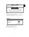
1-6 english english-1 declaration declaration of the manufacturer to prevent fire or shock hazards, do not expose this unit to rain or moisture. Also, do not use this unit’s polarized plug with an extension cord receptacle or other outlets unless the prongs can be fully inserted. Refrain from openin...
Page 10
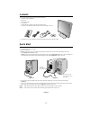
1-7 english-2 contents your new nec lcd monitor box* should contain the following: • lcd1501 monitor with tilt base • power cord • video signal cable • user’s manual • cd rom (includes complete user’s manual in pdf format). To see the user’s manual, acrobat reader 4.0 must be installed on your pc. *...
Page 11
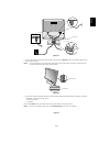
1-8 english english-3 figure c.1 figure d.1 6. The vacation switch on the right side of the monitor must be turned on (figure d.1). Turn on the monitor with the power button and the computer. Note: the vacation switch is a true on/off switch. If this switch is on the off position, the monitor cannot...
Page 12
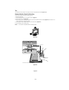
1-9 english-4 tilt grasp both sides of the monitor screen with your hands and adjust the tilt as desired (figure ts.1). Remove monitor stand for mounting to prepare the monitor for alternate mounting purposes: 1. Disconnect all cables. 2. Place monitor face down on a non-abrasive surface (figure r.1...
Page 13
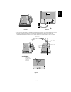
1-10 english english-5 7. This lcd monitor is designed for use with a flexible arm. Please use the attached screws (4pcs) when mounting. To meet the safety requirements the monitor must be mounted to an arm which guaranties the necessary stability under consideration of the weight of the monitor. Th...
Page 14
1-11 english-6 controls osm (on-screen-manager) controls the osm controls on the front of the monitor function as follows: to access osm press any of the control buttons (, >, -, +, exit). Note: when reset is pressed in the main and sub-menu, a warning window will appear allowing you to cancel the r...
Page 15
1-12 english english-7 fine improves focus, clarity and image stability by increasing or decreasing this setting. Should the “auto adjust function” and the “h.Size” function do not give you a satisfactory picture setting, a fine tuning can be performed using the “fine” function. It improves focus, c...
Page 16
1-13 english-8 information display mode indicates the current display resolution and frequency setting of the monitor. Monitor info. Indicates the model and serial numbers of your monitor. Osm warning osm warning menus disappear with exit button. No signal: this function gives a warning when there i...
Page 17
1-14 english english-9 recommended use safety precautions and maintenance for optimum performance, please note the following when setting up and using the lcd colour monitor: • do not open the monitor. There are no user serviceable parts inside and opening or removing covers may expose you to danger...
Page 18
1-15 english-10 • avoid displaying fixed patterns on the monitor for long periods of time to avoid image persistence (after-image effects). • get regular eye checkups. Ergonomics to realize the maximum ergonomics benefits, we recommend the following: • use the preset size and position controls with ...
Page 19
1-16 printed on recycled paper.
Page 20: Serial Number Information
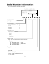
2-1 serial number information refer to the serial number information shown below. G g g g g g g g g g manufactured year : ( last digit ) manufactured month : january to september 1 to 9 october x november y december z classification code : discriminate by cabinet color white : 0 black : 1 gray(silve...
Page 21: Disassembly
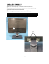
3-1 disassembly gbefore you disassembly the set, turn off power and pull out the power plug. G use the proper screwdriver. If oversize or undersize is used, screws may be damaged. G assembly is the opposite process of disassembly. G note: if consignment the parts begins, the part number of npg is us...
Page 22
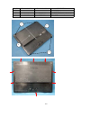
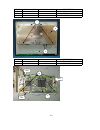
3-2 symbol part no. For npg part no. For nmv description 3 --- --- p3*8 ml(ni) 4 --- --- t3*16/w mc(ni) 5 10103231 79pq5102 cover rear assy(lcd1501bk 6 12300511 79en0526 vesa,bkt 4 5 6 3.
Page 23
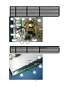
3-3 symbol part no. For npg part no. For nmv description 7 --- --- p3*6/w ml(ni) 8 --- --- 4#-40t*40t*4.8hl*4.0*5-nl/w 9 --- --- shield,cover symbol part no. For npg part no. For nmv description 10 --- --- p3*8*8+spw+was ml(ni) 11 am0r31ml 79pq5080 main insert assy 9 7 8 11 j301 j101 j601 10
Page 24
3-4 symbol part no. For npg part no. For nmv description 12 --- --- p3*8*8+spw+gear ml(ni) 13 --- --- f3*8 ml(ni) 14 --- --- p4*6+spw+was mc(ni) 15 ap0r31ml 79pq5081 power insert assy 16 jm100021 79pq5128 inverter bd. T301001.00 17 rc900051 79pq5160 lead connector assy-sw blk symbol part no. For npg...
Page 25
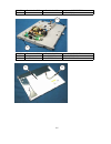
3-5 symbol part no. For npg part no. For nmv description 22 --- --- p2.5*4 mc(ni) symbol part no. For npg part no. For nmv description 23 --- 3a684033 lcd lm150x06-a3 24 rc200131 79pq5163 wire 20p-20p l120 22 22 21 22.
Page 26
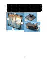
3-6 symbol part no. For npg part no. For nmv description 25 --- --- p4*8/w (ni) 26 --- --- t4*6 ml(ni) 27 12300841 79pq5164 shield base 28 17001241 79pq5165 pad foot 29 11001621 79pq5158 tile base 30 --- --- screw t3*10 25 26 27 28 28 29 30
Page 27
3-7 symbol part no. For npg part no. For nmv description 31 11001661 79pq5112 cover stand rear(bk) 32 14900031 --- hinge unit 33 11001651 79pq5111 cover stand front(bk) 34 11001671 79pq5109 cover cable(bk) 35 11301481 --- pad,hinge 36 11001631 79pq5110 cover hinge(t)(bk) 7 31 32 33 34 35 36.
Page 28: Adjustment Procedures
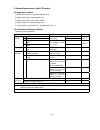
4-1 adjustment procedures table of contents page 1. Application ........................................................................................................................... 4-2 2. Default setting ............................................................................................
Page 29
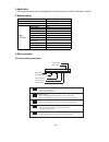
4-2 1. Application this adjustment specification shall be applied to the adjustment of the lcd1501 (model no. Nl2501). 2. Default setting item condition power supply ac100v~240v input freq. 1024 ×768@75hz brightness 100% contrast 50% color temp. Native osm trun off 30 sec. Osm look out no resolution...
Page 30
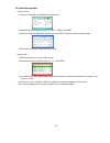
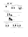
4-3 3.2 special key operation 1) open the information tab [mode] of the osm menu. 2) simultaneously press the three keys of (right), and reset. 3) when a message of warning appears, press the select button to enter the factory mode. 4) press the exit button to close the factory mode. 1) make the set...
Page 31
4-4 4. Adjustment 4.1 measuring instruments, jigs, and tools the measuring instruments, jigs, and tools required at the time of the adjustment of the unit to be adjusted shall be as specified below. A. A signal generator that can generate an output of signal timing produced by the adjusted (*) vg-81...
Page 32
4-5 5. Vg-819 setting values signal vg-819 mode 1024 ×768 (75hz) dot clock [mhz] 78.75 total [dot] 1312 disp [dot] 1024 sync pulse [dot] 96 back [dot] 176 hdstrat [dot] 0 h hdwidth [dot] 0 interlace non total [h] 800 disp [h] 768 sync pulse [h] 3 back porch [h] 28 eqpfp [h] 0 eqpbp [h] 0 serration [...
Page 33
4-6 6. Explanations of the factory mode on: accumulated time during the reception of input signals (led: green) off: accumulated time in the power-saving mode (led: amber) * the above-mentioned accumulated time (hours running) is reset when factory preset or the reset + “” keys is pushed during a di...
Page 34
4-7 it is possible to change the display of osd adjusting values. 0: adjusting value displayed in percentage: setting for shipment 1: adjusting value displayed in a numeral: (debug) the osd/osm display is changed over for the osd menu. 0: osm (setting for shipment) 1: osd display or no display of ur...
Page 35: Inspection
5-1 inspection table of contents page 1. Electrical inspection ............................................................................................................. 5-2 1.1 electrical performance ...................................................................................................
Page 36
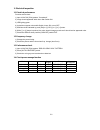
5-2 1. Electrical inspection 1.1 electrical performance function switch check 1) input 1024×768 (75hz) pattern “crosshatch”. 2) image should appeared within 4sec after switch on. 3) led lighting green. 4) it should not appear noise while switch is turn on or turn off. 5) osm should be indicated by p...
Page 37
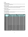
5-3 2. Safety 2.1 insulation resistance the resistance of the insulation between the power terminal and the earth ground contact is more than 10m ohms while withstanding a voltage of 500vdc. 2.2 dielectric strength there is no breakdown of the insulators or short circuits when applying an alternatin...
Page 38
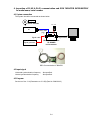
5-4 4. Inspection of plug & play communication and osm "monitor information" for model name/ serial number 4.1 system connection this system should be connected as shown below. Ddc communication i/f board signal cable signal cable printer cable (jig) signal generator desktop/note pc monitor program ...
Page 39
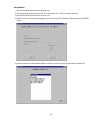
5-5 4.4 operation 1) connect the edid data writing unit with jigs, etc. 2) copy all the files of the service tool ver. 3.14 (parameter ver. 2.0-s2) in a proper directory. 3) start [service2.Exe] of the service tool ver. 3.14. 4) when the screen as shown below appears, give a check to [lcd] of [monit...
Page 40
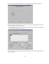
5-6 6) when the screen as shown below appears, give a check to [edid_read] and press the [ok] button. 7) when the screen as shown below appears, confirm that the correct data are displayed in the columns of edid data contents and serial information. If all the displayed data are [ff] or the like, or...
Page 41
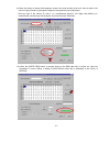
5-7 9) when the screen as shown below appears, examine the serial number of the unit, enter an input in the column of [input serial no.] through the keyboard, and press the [input ok] button. Enter an input in the column of [.Year=> ] in manufactured year(a.D. Four digits) and [month=>] in manufactu...
Page 42
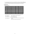
5-8 11) let the power switch of the writing unit be turned off/on, and examine the serial number column of the osd [monitor info.] to see that its contents have been changed to the updated serial number. 12) upon the normal completion of edid data writing, press the [exit] button to close the progra...
Page 43
5-9 5. External inspection on the lcd module 5.1 inspection condition 1) ambient temperature is approximately 20~25 °c. 2) ambient humidity is approximately 65 ±. 3) ambient illuminant is from 300 to 700lux. 4) viewing distance is approximately 35cm. 5) viewing angle : right and left 30 °, top and b...
Page 44
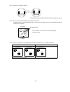
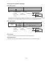
5-10 note 1: r + g, 2 dots continued horizontally counted as an ng not counted as ng and others note 2: (1) + (2) ≤ 3 pairs note 3: 3-defect combination combination patterns to be counted as ng / combination of all bright or all black dots and others not counted as ng / combination of bright and bla...
Page 45
5-11 note 6: approach of adjacent defects the distance between adjacent defects shall be longer than 10mm. Note 7: a set of 2 or more dot defects in an area of 5 ×5 pixels if there are two or more dot defects [(5)] in an area of 5 ×5 pixels, such a set of dot defects shall be counted as one cluster....
Page 46
5-12 5.3 the inspection standard of appearance 5.3.1 polarizer defects items criteria scratch linear 0.05 ≤ w ≤ 0.2, 5.0 ≤ l ≤ 10.0, n ≤ 4 dent circuar 0.2 ≤ d ≤ 0.5, n ≤ 6 note: d: average diameter d=(a+b)/2 w: width, l: length, n: quantity linear: a>2b, circular: a unit: mm a. Extraneous substance...
Page 47: Troubleshooting
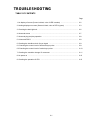
6-1 troubleshooting table of contents page 1. No display of screen (screen is black, color of led is amber) ........................................ 6-2 2. Nothing displays on screen (screen is black, color of led is green) .............................. 6-3 3. Checking the back light unit ............
Page 48
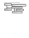
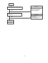
6-2 1. No display of screen (screen is black, color of led is amber) when a signal isn't being inputted, it is indicated with "no signal". It is indicated with "out of range" at the time of the frequency that it over spec. Timing. Yes ng ok proceed section 2 “nothing display on screen” check if the ...
Page 49
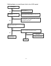
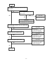
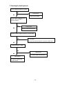
6-3 2. Nothing displays on screen (screen is black, color of led is green) ng ok ng ok ok ng ng ok refer to section 3 “checking the backlight unit. Does computer output rgb video signals? 1) change pattern of video signal output on the host. 2) reconnect the video cable. 3) change the video cable. C...
Page 50
6-4 ok ok ok ok ng ng ng ng ng continue is 3.3v voltage provided to pins 19 and 20 of j301 in main board? Is 3.3v voltage provided to pin 19 and 20 of j301. Ok failure point failure point check the de pulse is output on r405? Check the pvd signal is ouput on r433 ? J301 cable pulled out or disconnec...
Page 51
6-5 continue check the phd signal is ouput on r432? Ok ng failure point 1) ic401 failure. 2) printed wire broke between u401 and ic301 pin27. 3) r432 or c315 failure. Check the data signal output on ic301 r, g, b data pin?. Ok ng failure point 1) ic401 failure. 2) printed wire broke between ic401, i...
Page 52
6-6 3. Checking the back light unit ng ng ok ng ok is 12v voltage provided to inverter? Failure point check the on/ff signal of equal “h” at cn1 pin6? Check inverter f1 open. Failure point f1 failure. Replace the inverter board. Failure point inverter cable disconnection. Ok 1) µ-p failure. 2) print...
Page 53
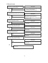
6-7 4. Abnormal screen ng ng ok ok check the r, g, b video signal from computer input on d-sub r,g,b connector. Failure point 1) no r, g and b video signal output from host computer. Check computer. 2) video signal cable disconnection. Check the r,b,g input signals on ic401 pin 2, 13, 20,respectivel...
Page 54
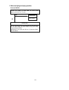
6-8 5. Abnormal plug and play operation abnormal ddc2b confirm the output of serial data on ic101 pin26 synchronize sclk at ttl level. Ng failure point ic101 failure. Failure point 1) the host machine isn't communicating in ddc2b mode. 2) the video cable may have failed or may not to have connection...
Page 55
6-9 6. Checking the interface circuit of sync signal 6.1 checking the control circuit of horizontal sync pulse check the horizontal sync signal on ic203 pin3 at ttl level. Ng ok failure point 1) no separate sync or composite sync output by host. (confirm the host, output the sync signal.) 2) video c...
Page 56
6-10 6.2 checking the control circuit of vertical sync pulse ng failure point 1) no separate sync output signal from the host.(check the host.) 2) video cable may have failed. 3) printed wire broke between j201 pin 14 and ic203 pin9 4) l209 or r213 open. 5) ic202 failure ok proceed section 7 “checki...
Page 57
6-11 7. Checking the resolution change ic movement is there +3.3v supply on ic401 pins 49, 57, 67, 79, 89, 101, 113, 125 ,132,143, 159. Is there +2.5v supply on ic401 pin 3, 6,14,17, 21,24, 26, 32, 38, 46, 71, 91, 103,123, 145,147, 152;is there +3.0v supply on ic401 pin8. Ng ok ng ok ok proceed sect...
Page 58
6-12 8. No power on check the +12v power provided from power board. Ng ok failure point power board failure. Check 3.3v power from ic601 ng ok failure point "checking the dc/dc converter circuit" proceed section 9 "checking the operation of cpu ".
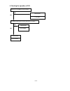
Page 59
6-13 9. Checking the operation of cpu is there +3.3v supply on ic101 pins 5. Ng ok failure point l110 open is 12mhz clock input to ic101 pin8, 9 at ttl level? Ng ok failure point x101 failure. Failure point ic101 failure..
Page 60: Circuit Description
7-1 circuit description table of contents page 1. Block diagram ...................................................................................................................... 7-2 2. Power circuit ...................................................................................................
Page 61
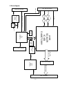
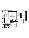
7-2 1. Block diagram j201; dsub connector j601; to power bd dc to dc ic601 tl494 12v i/p 3.3v o/p 2.5v reg. Ic402 up ic101 nt68f632 inverter control signal v sync. Adc scaler ic401 saa6713ah 12mhz; x101 eeprom ic102 24c16 25mhz;osc x401 j101; to key control bd h v h sync. Ic203 r,g,b ddc sda ddc scl...
Page 62
7-3 2. Power circuit 2.1 power input 12v dc input from power board through j601 to interface. 2.2 dc to dc circuit ic610 is used generate the system power. It have built in 1 channel pwm controller to provide voltage output. The output (3.3v) is provide panel vcc and 2.5v regulator input. And provid...
Page 63
7-4 3. Microprocessor control circuit 3.1 clock circuit the x101 is crystal ;it generates an 12mhz output for microprocessor. 3.2 i 2 c buses ic101 (pin 12) sda serial data ic101 (pin 13) scl serial clock this is i 2 c serial communication bus and is used for read or write data communication of ic10...
Page 64: Replacement Parts List
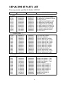
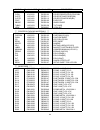
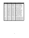
Replacement parts list the components specified for model lcd1501 symbol part no for npg part no for nmv description *** ics *** ic101 eha10341 79pq5134 ic plcc nt68f632 mcu 8bit ic102 eha10391 79pq5137 ic smd m24c16-wmn6 eeprom ic203 eha50011 79en0560 ic mos 74lvc14 ic301 eha10381 79pq5136 ic smd t...
Page 65
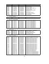
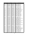
Symbol part no for npg part no for nmv description d601 ex500114 79en0592 diode/t chip 1ss355te-17 d602 ex700411 79pq5027 diode ssm24 d603 eyd40562 79en0598 zd chip udzs5.6b te-17 d605 ex700411 79pq5027 diode ssm24 d803 el200110 79en0573 diode led sml19460c d901 ej300115 79en0570 diode sf13 d902 ej1...
Page 66
Symbol part no for npg part no for nmv description l204 hm011011 79en0677 ferrite blm18ag121sn1 l206 hm011011 79en0677 ferrite blm18ag121sn1 l208 hm011532 79en0680 ferrite chip bk2125hs431 l209 hm011532 79en0680 ferrite chip bk2125hs431 l211 hm011011 79en0677 ferrite blm18ag121sn1 l301 hm011011 79en...
Page 67
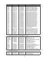
Symbol part no for npg part no for nmv description cvhnt 11001631 79pq5110 cover hinge(t)(bk) cvra 10103231 79pq5102 cover rear assy(lcd1501bk cvstf 11001651 79pq5111 cover stand front(bk) cvstr 11001661 79pq5112 cover stand rear(bk) foot 17001241 79pq5165 pad foot sbase 12300841 79pq5164 shield bas...
Page 68
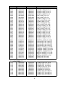
Symbol part no for npg part no for nmv description r206 fm010473 79pq5039 chip 1/10w(t) 5% 47k r207 fm010473 79pq5039 chip 1/10w(t) 5% 47k r209 fm010000 79en0175 r smd 1/10w(t) 5% 0 r210 fm010000 79en0175 r smd 1/10w(t) 5% 0 r211 fm100101 79pq1891 chip 1/8w(t) 5% 100h r212 fm010101 79en0615 r chip 1...
Page 69
Symbol part no for npg part no for nmv description r434 fm100330 79pq5043 r smd metal 1/8w 33h j r435 fm010472 79en0185 r smd 1/10w(t) 5% 4.7k r445 fm010472 79en0185 r smd 1/10w(t) 5% 4.7k r601 fm010472 79en0185 r smd 1/10w(t) 5% 4.7k r602 fm010102 79en0180 r smd 1/10w(t) 5% 1k r603 fm100000 79pq189...
Page 70
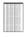
Symbol part no for npg part no for nmv description c113 gm410353 79en0503 c smd x7r/t 0.01u/50v k c114 gm410353 79en0503 c smd x7r/t 0.01u/50v k c115 gm410353 79en0503 c smd x7r/t 0.01u/50v k c116 gm410353 79en0503 c smd x7r/t 0.01u/50v k c117 gm410353 79en0503 c smd x7r/t 0.01u/50v k c118 gm410353 ...
Page 71
Symbol part no for npg part no for nmv description c421 gm433333 79pq5153 c cera x7r/t 0.033u/16v k c422 gm422333 79pq5152 c cera x7r/t 0.022u/16v k c423 gm433333 79pq5153 c cera x7r/t 0.033u/16v k c424 gm433333 79pq5153 c cera x7r/t 0.033u/16v k c425 gm433333 79pq5153 c cera x7r/t 0.033u/16v k c426...
Page 72
Symbol part no for npg part no for nmv description c622 gm410353 79en0503 c smd x7r/t 0.01u/50v k c623 gm410353 79en0503 c smd x7r/t 0.01u/50v k c902 gj033417 79pq5051 c safety-x 0.33u/275v m c903 gjc10285 79en0655 c safety y/d 1000p/250v m c904 gjc10285 79en0655 c safety y/d 1000p/250v m c905 gay00...
Page 73
9-1 block diagram interface board j201; dsub connector j601; to power bd dc to dc ic601 tl494 12v i/p 3.3v o/p 2.5v reg. Ic402 up ic101 nt68f632 inverter control signal v sync. Adc scaler ic401 saa6713ah 12mhz; x101 eeprom ic102 24c16 sdascl 25mhz;osc x401 j101; to key control bd h v h sync. Ic203 r...
Page 74
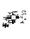
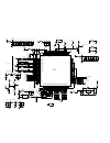
Tx0- tx3+ tx2+ tx1+ txc+ txc- tx2- tx3- tx1- tx0+ ro0 ro4 bo7 ro1 ro2 ro3 ro5 ro6 ro7 bo0 bo1 bo2 bo3 bo4 bo5 bo6 bo2 bo1 ro4 ro5 go5 ro0 bo3 go0 bo5 go6 go3 bo7 go4 bo4 bo6 go2 ro3 ro7 ro2 go7 ro1 bo0 go1 ro6 go0 go3 go4 go6 go1 go7 go2 go5 pvcc pvcc pvcc tx0- tx0+ tx1- tx2+ txc- tx3+ tx1+ tx2- txc...
Page 75
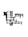
1/10 w led_r sda scl l e d _ r _ ct l sda led_g led_r_ctl reset led_g_ctl scl l e d _ g _ c t l led_g next reset right led_r minus left exit plus p lu s le f t soft_pw n e x t e x it r ig h t m in u s soft_pw wp wp scl lvdspwr dvi_detn v g a _s d a (1) v g a _s c l (1) tp_ctl d v i_ s c l (1) scaler...
Page 76
Power switch reserve reserve pwr_en +3_3v v re f +3_3v v re f vref vref +3_3v pwr_en tp_pwr t p _p w r backlig_on_off 1 pwr_sw 1 brightness 4 tp_ctl 12vin +5vp +5vp +5vp +5vp 12vin 12vin 12vin 5vd 3v3d 12vin +5vp + c602 470u 25v 1 2 d601 1ss355 1 2 r617 1k 1 2 d602 ssm24 1 2 c608 1u 10v 1 2 r615 10k...
Page 77
A s c lose as possible t h e scaler chip csg2 g o 7 g o 5 g o 4 g o 3 g o 2 g o 1 g o 0 g o 6 clk_25m csg2 c s g 4 pwm csg4 ro5 ro1 ro4 ro0 ro7 ro2 ro6 ro3 b o 4 b o 1 b o 7 b o 2 b o 6 b o 3 b o 0 b o 5 +2v5 +2v5 pvd phd pclk 2 scaler_intn 1 scaler_rstn 1 scl 1 b_in 5 g_in 5 r_in 5 brightness 3 go[...
Page 78
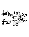
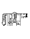
V h g_in 4 r_in 4 av 4 b_in 4 vga_sda vga_scl ah 4 pc_det agnd agnd agnd agnd agnd agnd agnd agnd agnd 3v3d agnd agnd 5vd 5vd 5vd 3v3d mcu_3_3v dvi_5v mcu_3_3v agnd agnd r207 47k 1 2 r206 47k 1 2 ic203c 74lvc14 5 6 14 7 l206 blm18ag121sn1 1 2 j201 vga-hdr/fm 1 9 2 10 3 11 4 12 5 13 6 14 7 15 8 17 16...
Page 79
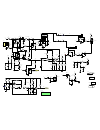
To main to inverter ac in 100v~240v main sw b2p3-vh-b 49a-1041 t901 ls-np02p-004 10 9 8 7 11 12 1 2 4 5 6 r921 470 1/2w pd901 p6ke200a c923 3300p meb r924 18.5k 1/4w 1% c911 0.01u 1kv npo c902 0.33uf-m 275v 12v 12v gnd gnd inv_on/off brt j932 1 2 3 4 5 6 7 c906 0.01u 1kv npo r922 1k 1/4w j901 1 2 3 ...
Page 80
1 2 r1 r/200/1206 1 2 r2 r/200/1206 1 2 r3 r/20k 1 2 r4 r/33k 1 2 r5 r/2k 1 2 r6 r/2k/0805 1 2 c1 c/104k 1 2 c2 c/nc 1 2 c4 c/0.22uf/160v 1 2 f1 f/icp-s2.3 1 2 + c5 c/220uf/25v 1 2 3 q1 q /3 90 4/ so t -2 3 3 4 2 5 6 1 q5 q/si3457dv 1 2 l1 l/33uh/k/61 1 2 d1 d /r l z 10 b /s o d -8 0 1 2 3 q6 q/2sc5...


