- DL manuals
- NEC
- Microcontrollers
- ?PD703302
- User Manual
NEC ?PD703302 User Manual
Summary of ?PD703302
Page 1
V850es/ke1+ 32-bit single-chip microcontrollers hardware printed in japan user’s manual μ pd703302 μ pd703302y μ pd70f3302 μ pd70f3302y 2004 document no. U16896ej2v0ud00 (2nd edition) date published august 2006 n cp(k).
Page 2
User’s manual u16896ej2v0ud 2 [memo].
Page 3
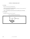
User’s manual u16896ej2v0ud 3 1 2 3 4 voltage application waveform at input pin waveform distortion due to input noise or a reflected wave may cause malfunction. If the input of the cmos device stays in the area between v il (max) and v ih (min) due to noise, etc., the device may malfunction. Take c...
Page 4
User’s manual u16896ej2v0ud 4 caution: μ pd70f3302 and 70f3302y use superflash ® technology licensed from silicon storage technology, inc. Iecube is a registered trademark of nec electronics corporation in japan and germany. Minicube is a registered trademark of nec electronics corporation in japan ...
Page 5
User’s manual u16896ej2v0ud 5 these commodities, technology or software, must be exported in accordance with the export administration regulations of the exporting country. Diversion contrary to the law of that country is prohibited. The information in this document is current as of february, 2006. ...
Page 6
User’s manual u16896ej2v0ud 6 preface readers this manual is intended for users who wish to understand the functions of the v850es/ke1+ and design application systems using these products. Purpose this manual is intended to give users an understanding of the hardware functions of the v850es/ke1+ sho...
Page 7
User’s manual u16896ej2v0ud 7 conventions data significance: higher digits on the left and lower digits on the right active low representation: xxx (overscore over pin or signal name) memory map address: higher addresses on the top and lower addresses on the bottom note: footnote for item marked wit...
Page 8
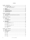
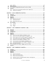
User’s manual u16896ej2v0ud 8 contents chapter 1 introduction..................................................................................................................17 1.1 k1 series product lineup ................................................................................................
Page 9
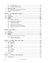
User’s manual u16896ej2v0ud 9 4.3.8 port dl ...........................................................................................................................................99 4.4 block diagrams ..................................................................................................
Page 10
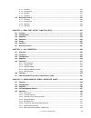
User’s manual u16896ej2v0ud 10 7.4.6 ppg output operation .................................................................................................................. 271 7.4.7 one-shot pulse output operation.........................................................................................
Page 11
User’s manual u16896ej2v0ud 11 11.1.1 functions ......................................................................................................................................347 11.1.2 configuration ................................................................................................
Page 12
User’s manual u16896ej2v0ud 12 14.6 dedicated baud rate generator n (brgn) ............................................................................ 424 14.6.1 baud rate generator n (brgn) configuration ............................................................................... 424 14.6.2 ser...
Page 13
User’s manual u16896ej2v0ud 13 16.13.2 when communication reservation function is disabled (iicf0.Iicrsv0 bit = 1) ...........................514 16.14 cautions.................................................................................................................................... 515 16....
Page 14
User’s manual u16896ej2v0ud 14 19.3.1 setting and operation status ........................................................................................................ 578 19.3.2 releasing halt mode.....................................................................................................
Page 15
User’s manual u16896ej2v0ud 15 23.1 function .................................................................................................................................... 618 23.2 configuration.......................................................................................................
Page 16
User’s manual u16896ej2v0ud 16 appendix a development tools............................................................................................... 680 a.1 software package..................................................................................................................... 683...
Page 17
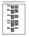
User’s manual u16896ej2v0ud 17 chapter 1 introduction 1.1 k1 series product lineup 1.1.1 v850es/kx1+, v850es/kx1 products lineup v850es/ke1 • 64-pin plastic lqfp (10 × 10 mm, 0.5 mm pitch) • 64-pin plastic tqfp (12 × 12 mm, 0.65 mm pitch) pd70f3207hy pd70f3207h single-power flash: 128 kb, ram: 4 kb ...
Page 18
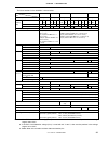
Chapter 1 introduction user’s manual u16896ej2v0ud 18 the function list of the v850es/kx1+ is shown below. Product name v850es/ke1+ v850es/kf1+ v850es/kg1+ v850es/kj1+ number of pins 64 pins 80 pins 100 pins 144 pins mask rom 128 − − 256 − − 256 − − − flash memory − 128 128 − 256 128 − 256 128 256 i...
Page 19
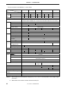
Chapter 1 introduction user’s manual u16896ej2v0ud 19 the function list of the v850es/kx1 is shown below. Product name v850es/ke1 v850es/kf1 v850es/kg1 v850es/kj1 number of pins 64 pins 80 pins 100 pins 144 pins mask rom 128 − 64/ 96 128 − 256 − 64/ 96 128 − 256 − 96/128 − − flash memory − 128 − − 1...
Page 20
Chapter 1 introduction user’s manual u16896ej2v0ud 20 1.1.2 78k0/kx1+, 78k0/kx1 products lineup mask rom: 24 kb, ram: 768 b mask rom: 16 kb, ram: 768 b mask rom: 8 kb, ram: 512 b pd780101 78k0/kb1 30-pin ssop (7.62 mm 0.65 mm pitch) single-power flash: 24 kb, ram: 768 b single-power flash: 16 kb, ra...
Page 21
Chapter 1 introduction user’s manual u16896ej2v0ud 21 the list of functions in the 78k0/kx1 is shown below. Part number item 78k0/kb1 78k0/kc1 78k0/kd1 78k0/ke1 78k0/kf1 number of pins 30 pins 44 pins 52 pins 64 pins 80 pins mask rom 8 16/ 24 − 8/ 16 24/ 32 − 8/ 16 24/ 32 − 8/ 16 24/ 32 − 48/ 60 − 2...
Page 22
Chapter 1 introduction user’s manual u16896ej2v0ud 22 the list of functions in the 78k0/kx1+ is shown below. Part number item 78k0/kb1+ 78k0/kc1+ 78k0/kd1+ 78k0/ke1+ 78k0/kf1+ number of pins 30 pins 44 pins 52 pins 64 pins 80 pins flash memory 8 16/24 16 24/32 16 24/32 16 24/32 48/60 60 internal mem...
Page 23
Chapter 1 introduction user’s manual u16896ej2v0ud 23 1.2 features { minimum instruction execution time: 50 ns (operation at main clock (f xx ) = 20 mhz) { general-purpose registers: 32 bits × 32 registers { cpu features: signed multiplication (16 × 16 → 32): 1 to 2 clocks (instructions without crea...
Page 24
Chapter 1 introduction user’s manual u16896ej2v0ud 24 { internal oscillator: 240 khz (typ.) remark for frequency characteristics (error) of internal oscillator, refer to chapter 28 electrical specifications. { reset • reset by reset pin • reset by overflow of watchdog timer 1 (wdtres1) • reset by ov...
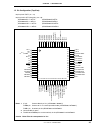
Page 25
Chapter 1 introduction user’s manual u16896ej2v0ud 25 1.5 pin configuration (top view) 64-pin plastic tqfp (12 × 12) 64-pin plastic lqfp (fine pitch) (10 × 10) μ pd703302gk- ×××-9et-a μ pd703302gb- ×××-8eu-a μ pd703302ygk- ×××-9et-a μ pd703302ygb- ×××-8eu-a μ pd70f3302gk-9et-a μ pd70f3302gb-8eu-a μ ...
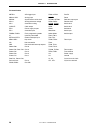
Page 26
Chapter 1 introduction user’s manual u16896ej2v0ud 26 pin identification adtrg: a/d trigger input ani0 to ani7: analog input asck0: asynchronous serial clock av ref0 : analog reference voltage av ss : ground for analog clkout: clock output ev dd : power supply for port ev ss : ground for port flmd0,...
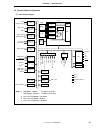
Page 27
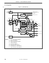
Chapter 1 introduction user’s manual u16896ej2v0ud 27 1.6 function block configuration (1) internal block diagram nmi to01 ti010, ti011 so00, so01 si00, si01 sck00, sck01 intp0 to intp7 intc top00, top01 tip00, tip01 to50, to51 ti50, ti51 toh0, toh1 txd0, txd1 rxd0, rxd1 asck0 rtp00 to rtp05 kr0 to ...
Page 28
Chapter 1 introduction user’s manual u16896ej2v0ud 28 (2) internal units (a) cpu the cpu uses five-stage pipeline control to enable single-clock execution of address calculations, arithmetic logic operations, data transfers, and almost all other types of instruction processing. Other dedicated on-ch...
Page 29
Chapter 1 introduction user’s manual u16896ej2v0ud 29 (i) watchdog timer two watchdog timer channels are provided on chip to detect program loops and system abnormalities. Watchdog timer 1 can be used as an interval timer. When used as a watchdog timer, it generates a non- maskable interrupt request...
Page 30
Chapter 1 introduction user’s manual u16896ej2v0ud 30 (q) power-on-clear (poc) circuit the power-on-clear circuit generates an internal reset signal at power on. The power-on-clear circuit compares the supply voltage (v dd ) and detection voltage (v poc ), and generates an internal reset signal when...
Page 31
Chapter 1 introduction user’s manual u16896ej2v0ud 31 1.7 overview of functions part number μ pd703302, 703302y μ pd70f3302, 70f3302y rom 128 kb 128 kb (single-power flash memory) internal memory high-speed ram 4 kb memory space 64 mb general-purpose registers 32 bits × 32 registers ceramic/crystal/...
Page 32
User’s manual u16896ej2v0ud 32 chapter 2 pin functions the names and functions of the pins of the v850es/ke1+ are described below, divided into port pins and non-port pins. The pin i/o buffer power supplies are divided into two systems; av ref0 and ev dd . The relationship between these power suppli...
Page 33
Chapter 2 pin functions user’s manual u16896ej2v0ud 33 (2/2) pin name pin no. I/o pull-up resistor function alternate function p50 28 ti011/rtp00/kr0 p51 29 ti50/rtp01/kr1 p52 30 to50/rtp02/kr2 p53 31 rtp03/kr3 p54 34 rtp04/kr4 p55 35 i/o yes port 5 i/o port input/output can be specified in 1-bit un...
Page 34
Chapter 2 pin functions user’s manual u16896ej2v0ud 34 (2) non-port pins (1/2) pin name pin no. I/o pull-up resistor function alternate function adtrg 24 input yes a/d converter external trigger input p32/asck0/to01 ani0 64 p70 ani1 63 p71 ani2 62 p72 ani3 61 p73 ani4 60 p74 ani5 59 p75 ani6 58 p76 ...
Page 35
Chapter 2 pin functions user’s manual u16896ej2v0ud 35 (2/2) pin name pin no. I/o pull-up resistor function alternate function rtp00 28 p50/ti011/kr0 rtp01 29 p51/ti50/kr1 rtp02 30 p52/to50/kr2 rtp03 31 p53/kr3 rtp04 34 p54/kr4 rtp05 35 output yes real-time output port p55/kr5 rxd0 23 serial receive...
Page 36
Chapter 2 pin functions user’s manual u16896ej2v0ud 36 2.2 pin i/o circuits and recommended connection of unused pins (1/2) pin alternate function pin no. I/o circuit type recommended connection p00 toh0 12 p01 toh1 13 5-a p02 nmi 14 p03 to p06 intp0 to intp3 15 to 18 5-w p30 txd0 22 5-a p31 rxd0/in...
Page 37
Chapter 2 pin functions user’s manual u16896ej2v0ud 37 (2/2) pin alternate function pin no. I/o circuit type recommended connection av ref0 – 1 – directly connect to v dd . Av ss – 2 – – ev dd – 33 – – ev ss – 32 – – ic note 1 – 3 – directly connect to ev ss or v ss or pull down with a 10 k Ω resist...
Page 38
Chapter 2 pin functions user’s manual u16896ej2v0ud 38 2.3 pin i/o circuits (1/2) type 2 type 8-a type 9-c type 5-a type 10-a type 5-w type 10-e schmitt-triggered input with hysteresis characteristics in data output disable p-ch in/out v dd n-ch input enable p-ch v dd pull-up enable in comparator + ...
Page 39
Chapter 2 pin functions user’s manual u16896ej2v0ud 39 (2/2) type 16 p-ch feedback cut-off xt1 xt2 type 13-ae data output disable input enable in/out n-ch v ss mask option v dd type 13-ad data output disable input enable in/out n-ch v ss remark read v dd as ev dd . Also, read v ss as ev ss ..
Page 40
User’s manual u16896ej2v0ud 40 chapter 3 cpu functions the cpu of the v850es/ke1+ is based on the risc architecture and executes most instructions in one clock cycle by using 5-stage pipeline control. 3.1 features { number of instructions: 83 { minimum instruction execution time: 50.0 ns (@ 20 mhz o...
Page 41
Chapter 3 cpu functions user’s manual u16896ej2v0ud 41 3.2 cpu register set the cpu registers of the v850es/ke1+ can be classified into two categories: a general-purpose program register set and a dedicated system register set. All the registers have 32-bit width. For details, refer to the v850es ar...
Page 42
Chapter 3 cpu functions user’s manual u16896ej2v0ud 42 3.2.1 program register set the program register set includes general-purpose registers and a program counter. (1) general-purpose registers (r0 to r31) thirty-two general-purpose registers, r0 to r31, are available. All of these registers can be...
Page 43
Chapter 3 cpu functions user’s manual u16896ej2v0ud 43 3.2.2 system register set system registers control the status of the cpu and hold interrupt information. Read from and write to system registers are performed by setting the system register numbers shown below with the system register load/store...
Page 44
Chapter 3 cpu functions user’s manual u16896ej2v0ud 44 (1) interrupt status saving registers (eipc, eipsw) there are two interrupt status saving registers, eipc and eipsw. Upon occurrence of a software exception or a maskable interrupt, the contents of the program counter (pc) are saved to eipc and ...
Page 45
Chapter 3 cpu functions user’s manual u16896ej2v0ud 45 (2) nmi status saving registers (fepc, fepsw) there are two nmi status saving registers, fepc and fepsw. Upon occurrence of a non-maskable interrupt (nmi), the contents of the program counter (pc) are saved to fepc and the contents of the progra...
Page 46
Chapter 3 cpu functions user’s manual u16896ej2v0ud 46 (4) program status word (psw) the program status word (psw) is a collection of flags that indicate the program status (instruction execution result) and the cpu status. When the contents of this register are changed using the ldsr instruction, t...
Page 47
Chapter 3 cpu functions user’s manual u16896ej2v0ud 47 (2/2) note during saturated operation, the saturated operation results are determined by the contents of the ov flag and s flag. The sat flag is set (to 1) only when the ov flag is set (to 1) during saturated operation. Flag status operation res...
Page 48
Chapter 3 cpu functions user’s manual u16896ej2v0ud 48 (6) exception/debug trap status saving registers (dbpc, dbpsw) there are two exception/debug trap status saving registers, dbpc and dbpsw. Upon occurrence of an exception trap or debug trap, the contents of the program counter (pc) are saved to ...
Page 49
Chapter 3 cpu functions user’s manual u16896ej2v0ud 49 3.3 operating modes the v850es/ke1+ has the following operating modes. (1) normal operating mode after the system has been released from the reset state, the pins related to the bus interface are set to the port mode, execution branches to the r...
Page 50
Chapter 3 cpu functions user’s manual u16896ej2v0ud 50 3.4 address space 3.4.1 cpu address space for instruction addressing, an internal rom area of up to 1 mb, and an internal ram area are supported in a linear address space (program space) of up to 64 mb. For operand addressing (data access), up t...
Page 51
Chapter 3 cpu functions user’s manual u16896ej2v0ud 51 3.4.2 wraparound of cpu address space (1) program space of the 32 bits of the program counter (pc), the higher 6 bits are fixed to 0 and only the lower 26 bits are valid. Even if a carry or borrow occurs from bit 25 to bit 26 as a result of bran...
Page 52
Chapter 3 cpu functions user’s manual u16896ej2v0ud 52 3.4.3 memory map the v850es/ke1+ has reserved areas as shown below. Figure 3-2. Data memory map (physical addresses) 3ffffffh 3fec000h 3febfffh 0100000h 00fffffh 0000000h 3fff000h 3ffefffh 3fff000h 3ffefffh 3ffffffh 3fec000h (80 kb) use-prohibit...
Page 53
Chapter 3 cpu functions user’s manual u16896ej2v0ud 53 figure 3-3. Program memory map 03ff0000h 03feffffh 03fff000h 03ffefffh 03ffffffh 00100000h 000fffffh 00000000h internal ram area (60 kb) use-prohibited area (program fetch disabled area) use-prohibited area (program fetch disabled area) internal...
Page 54
Chapter 3 cpu functions user’s manual u16896ej2v0ud 54 3.4.4 areas (1) internal rom area an area of 1 mb from 0000000h to 00fffffh is reserved for the internal rom area. (a) internal rom (128 kb) a 128 kb area from 0000000h to 001ffffh is provided in the v850es/ke1+. Addresses 0020000h to 00fffffh a...
Page 55
Chapter 3 cpu functions user’s manual u16896ej2v0ud 55 (3) on-chip peripheral i/o area a 4 kb area from 3fff000h to 3ffffffh is reserved as the on-chip peripheral i/o area. Figure 3-6. On-chip peripheral i/o area 3ffffffh 3fff000h on-chip peripheral i/o area (4 kb) fffffffh ffff000h physical address...
Page 56
Chapter 3 cpu functions user’s manual u16896ej2v0ud 56 3.4.5 recommended use of address space the architecture of the v850es/ke1+ requires that a register that serves as a pointer be secured for address generation when operand data in the data space is accessed. The address stored in this pointer ±3...
Page 57
Chapter 3 cpu functions user’s manual u16896ej2v0ud 57 figure 3-7. Recommended memory map data space program space on-chip peripheral i/o on-chip peripheral i/o internal ram internal ram internal rom use prohibited use prohibited internal ram on-chip peripheral i/o note program space 64 mb internal ...
Page 58
Chapter 3 cpu functions user’s manual u16896ej2v0ud 58 3.4.6 peripheral i/o registers (1/7) operable bit unit address function register name symbol r/w 1 8 16 after reset fffff004h port dl register pdl r/w √ √ 00h note 1 fffff00ch port cm register pcm r/w √ √ 00h note 1 fffff024h port dl mode regist...
Page 59
Chapter 3 cpu functions user’s manual u16896ej2v0ud 59 (2/7) operable bit unit address function register name symbol r/w 1 8 16 after reset fffff148h interrupt control register wtiic r/w √ √ 47h fffff14ah interrupt control register wtic r/w √ √ 47h fffff14ch interrupt control register brgic r/w √ √ ...
Page 60
Chapter 3 cpu functions user’s manual u16896ej2v0ud 60 (3/7) operable bit unit address function register name symbol r/w 1 8 16 after reset fffff446h port 3 mode control register pmc3 r/w √ 0000h fffff446h port 3 mode control register l pmc3l r/w √ √ 00h fffff447h port 3 mode control register h pmc3...
Page 61
Chapter 3 cpu functions user’s manual u16896ej2v0ud 61 (4/7) operable bit unit address function register name symbol r/w 1 8 16 after reset fffff5c6h 16-bit timer mode control register 5 tmc5 r/w √ 0000h fffff5c6h 8-bit timer mode control register 50 tmc50 r/w √ √ 00h fffff5c7h 8-bit timer mode cont...
Page 62
Chapter 3 cpu functions user’s manual u16896ej2v0ud 62 (5/7) operable bit unit address function register name symbol r/w 1 8 16 32 after reset fffff820h power save mode register psmr r/w √ √ 00h fffff828h processor clock control register pcc r/w √ √ 03h fffff82eh cpu operation clock status register ...
Page 63
Chapter 3 cpu functions user’s manual u16896ej2v0ud 63 (6/7) operable bit unit address function register name symbol r/w 1 8 16 after reset fffffb00h tip00 noise elimination control register p0nfc r/w √ √ 00h fffffb04h tip01 noise elimination control register p1nfc r/w √ √ 00h fffffc00h external int...
Page 64
Chapter 3 cpu functions user’s manual u16896ej2v0ud 64 (7/7) operable bit unit address function register name symbol r/w 1 8 16 after reset fffffd1ah serial i/o shift register 1 sio01 r/w √ 00h fffffd1ah serial i/o shift register 1l sio01l r/w √ 0000h fffffd80h iic shift register 0 iic0 note r/w √ 0...
Page 65
Chapter 3 cpu functions user’s manual u16896ej2v0ud 65 3.4.7 special registers special registers are registers that prevent invalid data from being written when an inadvertent program loop occurs. The v850es/ke1+ has the following six special registers. • power save control register (psc) • processo...
Page 66
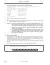
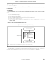
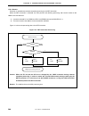
Chapter 3 cpu functions user’s manual u16896ej2v0ud 66 [description example] when using psc register (standby mode setting) st.B r11, psmr[r0] ; psmr register setting (idle, stop mode setting) mov 0x02, r10 st.B r10, prcmd[r0] ; prcmd register write st.B r10, psc[r0] ; psc register setting nop note ...
Page 67
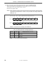
Chapter 3 cpu functions user’s manual u16896ej2v0ud 67 (3) system status register (sys) this register is allocated with status flags showing the operating state of the entire system. This register can be read or written in 8-bit or 1-bit units. 0 protection error has not occurred protection error ha...
Page 68
Chapter 3 cpu functions user’s manual u16896ej2v0ud 68 3.4.8 cautions (1) wait when accessing register be sure to set the following register before using the v850es/ke1+. • system wait control register (vswc) after setting the vswc register, set the other registers as required. When using an externa...
Page 69
Chapter 3 cpu functions user’s manual u16896ej2v0ud 69 peripheral function register name access k wdtm1 write 1 to 5 watchdog timer 1 (wdt1) note 1 > k = {(1/f x ) × 2/((2 + m)/f cpu )} + 1 f x : main clock oscillation frequency watchdog timer 2 (wdt2) wdtm2 write 3 (fixed) tp0ccr0, tp0ccr1, tp0cnt ...
Page 70
Chapter 3 cpu functions user’s manual u16896ej2v0ud 70 (2) restriction on conflict between sld instruction and interrupt request (a) description if a conflict occurs between the decode operation of an instruction in immediately before the sld instruction following an instruction in and an interrupt ...
Page 71
User’s manual u16896ej2v0ud 71 chapter 4 port functions 4.1 features { input-only ports: 8 pins { i/o ports: 43 pins • fixed to n-ch open-drain output: 2 • switchable to n-ch open-drain output: 4 { input/output can be specified in 1-bit units 4.2 basic port configuration the v850es/ke1+ incorporates...
Page 72
Chapter 4 port functions user’s manual u16896ej2v0ud 72 4.3 port configuration table 4-2. Port configuration item configuration control registers port n register (pn: n = 0, 3 to 5, 7, 9, cm, dl) port n mode register (pmn: n = 0, 3 to 5, 9, cm, dl) port n mode control register (pmcn: n = 0, 3 to 5, ...
Page 73
Chapter 4 port functions user’s manual u16896ej2v0ud 73 (1) port n register (pn) data i/o with external devices is performed by writing to and reading from the pn register. The pn register is configured of a port latch that retains the output data and a circuit that reads the pin status. Each bit of...
Page 74
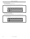
Chapter 4 port functions user’s manual u16896ej2v0ud 74 (2) port n mode register (pmn) pmn specifies the input mode/output mode of the port. Each bit of the pmn register corresponds to one pin of port n and can be specified in 1-bit units. Pmn7 output mode input mode pmnm 0 1 control of i/o mode pmn...
Page 75
Chapter 4 port functions user’s manual u16896ej2v0ud 75 (4) port n function control register (pfcn) pfcn is a register that specifies the alternate function to be used when one pin has two or more alternate functions. Each bit of the pfcn register corresponds to one pin of port n and can be specifie...
Page 76
Chapter 4 port functions user’s manual u16896ej2v0ud 76 (6) port n function register (pfn) pfn is a register that specifies normal output/n-ch open-drain output. Each bit of the pfn register corresponds to one pin of port n and can be specified in 1-bit units. Pfn7 pfn6 pfn5 pfn4 pfn3 pfn2 pfn1 pfn0...
Page 77
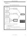
Chapter 4 port functions user’s manual u16896ej2v0ud 77 (8) port settings set the ports as follows. Figure 4-1. Register settings and pin functions pmcn register output mode input mode pmn register “ 0 ” “ 1 ” “ 0 ” “ 1 ” “ 0 ” “ 1 ” (a) (b) (c) (d) alternate function (when two alternate functions a...
Page 78
Chapter 4 port functions user’s manual u16896ej2v0ud 78 4.3.1 port 0 port 0 is a 7-bit i/o port for which i/o settings can be controlled in 1-bit units. Port 0 includes the following alternate functions. Table 4-4. Alternate-function pins of port 0 pin no. Pin name alternate function i/o pull note 1...
Page 79
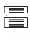
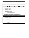
Chapter 4 port functions user’s manual u16896ej2v0ud 79 (3) port 0 mode control register (pmc0) 0 pmc0 pmc06 pmc05 pmc04 pmc03 pmc02 pmc01 pmc00 i/o port intp3 input pmc06 0 1 specification of p06 pin operation mode i/o port intp2 input pmc05 0 1 specification of p05 pin operation mode i/o port intp...
Page 80
Chapter 4 port functions user’s manual u16896ej2v0ud 80 4.3.2 port 3 port 3 is an 8-bit i/o port for which i/o settings can be controlled in 1-bit units. Port 3 includes the following alternate functions. Table 4-5. Alternate-function pins of port 3 pin no. Pin name alternate function i/o pull note ...
Page 81
Chapter 4 port functions user’s manual u16896ej2v0ud 81 (1) port 3 register (p3) 0 is output 1 is output p3n 0 1 control of output data (in output mode) (n = 0 to 5, 8, 9) p3 (p3h note ) after reset: 00h (output latch) r/w address: p3 fffff406h, p3l fffff406h, p3h fffff407h 0 0 p35 p34 p33 p32 p31 p...
Page 82
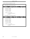
Chapter 4 port functions user’s manual u16896ej2v0ud 82 (3) port 3 mode control register (pmc3) pmc3 (pmc3h note 1 ) i/o port scl0 i/o pmc39 0 1 specification of p39 pin operation mode i/o port sda0 i/o pmc38 0 1 specification of p38 pin operation mode i/o port ti010 input/to01 output pmc35 0 1 spec...
Page 83
Chapter 4 port functions user’s manual u16896ej2v0ud 83 (4) port 3 function register h (pf3h) 0 when used as normal port (n-ch open-drain output) when used as alternate-function (n-ch open-drain output) pf3n 0 1 specification of normal port/alternate function (n = 8, 9) pf3h 0 0 0 0 0 pf39 pf38 afte...
Page 84
Chapter 4 port functions user’s manual u16896ej2v0ud 84 (7) specifying alternate-function pins of port 3 pfc35 specification of alternate-function pin of p35 pin 0 ti010 input 1 to01 output pfce34 pfc34 specification of alternate-function pin of p34 pin 0 0 setting prohibited 0 1 setting prohibited ...
Page 85
Chapter 4 port functions user’s manual u16896ej2v0ud 85 4.3.3 port 4 port 4 is a 3-bit i/o port for which i/o settings can be controlled in 1-bit units. Port 4 includes the following alternate functions. Table 4-6. Alternate-function pins of port 4 pin no. Pin name alternate function i/o pull note r...
Page 86
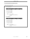
Chapter 4 port functions user’s manual u16896ej2v0ud 86 (3) port 4 mode control register (pmc4) 0 pmc4 0 0 0 0 pmc42 pmc41 pmc40 i/o port sck00 i/o pmc42 0 1 specification of p42 pin operation mode i/o port so00 output pmc41 0 1 specification of p41 pin operation mode i/o port si00 input pmc40 0 1 s...
Page 87
Chapter 4 port functions user’s manual u16896ej2v0ud 87 4.3.4 port 5 port 5 is a 6-bit i/o port for which i/o settings can be controlled in 1-bit units. Port 5 includes the following alternate functions. Table 4-7. Alternate-function pins of port 5 pin no. Pin name alternate function i/o pull note r...
Page 88
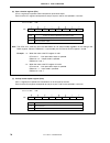
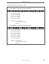
Chapter 4 port functions user’s manual u16896ej2v0ud 88 (3) port 5 mode control register (pmc5) i/o port/kr5 input rtp05 output pmc55 0 1 specification of p55 pin operation mode i/o port/kr4 input rtp04 output pmc54 0 1 specification of p54 pin operation mode 0 0 pmc55 pmc54 pmc53 pmc52 pmc51 pmc50 ...
Page 89
Chapter 4 port functions user’s manual u16896ej2v0ud 89 (4) port 5 function control register (pfc5) caution when the p5n pin is specified as an alternate function by the pmc5.Pmc5n bit with the pfc5n bit maintaining the initial value (0), output becomes undefined. Therefore, to specify the p5n pin a...
Page 90
Chapter 4 port functions user’s manual u16896ej2v0ud 90 4.3.5 port 7 port 7 is an 8-bit input-only port for which all the pins are fixed to input. Port 7 includes the following alternate functions. Table 4-8. Alternate-function pins of port 7 pin no. Pin name alternate function i/o pull note remark ...
Page 91
Chapter 4 port functions user’s manual u16896ej2v0ud 91 4.3.6 port 9 port 9 is a 9-bit i/o port for which i/o settings can be controlled in 1-bit units. Port 9 includes the following alternate functions. Table 4-9. Alternate-function pins of port 9 pin no. Pin name alternate function i/o pull note r...
Page 92
Chapter 4 port functions user’s manual u16896ej2v0ud 92 (1) port 9 register (p9) 0 is output 1 is output p9n 0 1 control of output data (in output mode) (n = 0, 1, 6 to 9, 13 to 15) after reset: 00h (output latch) r/w address: p9 fffff412h, p9l fffff412h, p9h fffff413h p915 p9 (p9h note ) p914 p913 ...
Page 93
Chapter 4 port functions user’s manual u16896ej2v0ud 93 (3) port 9 mode control register (pmc9) i/o port intp6 input pmc915 0 1 specification of p915 pin operation mode pmc97 pmc96 0 0 0 0 pmc91 pmc90 after reset: 0000h r/w address: pmc9 fffff452h, pmc9l fffff452h, pmc9h fffff453h pmc915 pmc9 (pmc9h...
Page 94
Chapter 4 port functions user’s manual u16896ej2v0ud 94 (4) port 9 function register h (pf9h) 0 normal output n-ch open-drain output pf9n 0 1 control of normal output/n-ch open-drain output (n = 8, 9) pf9h 0 0 0 0 0 pf99 pf98 after reset: 00h r/w address: fffffc73h caution when using p98 and p99 as ...
Page 95
Chapter 4 port functions user’s manual u16896ej2v0ud 95 (5) port 9 function control register (pfc9) caution when port 9 is specified as an alternate function by the pmc9.Pmc9n bit with the pfc9n bit maintaining the initial value (0), output becomes undefined. Therefore, to specify port 9 as alternat...
Page 96
Chapter 4 port functions user’s manual u16896ej2v0ud 96 (6) pull-up resistor option register 9 (pu9) not connected connected pu9n 0 1 control of on-chip pull-up resistor connection (n = 0, 1, 6 to 9, 13 to 15) pu9 (pu9h note ) after reset: 0000h r/w address: pu9 fffffc52h, pu9l fffffc52h, pu9h fffff...
Page 97
Chapter 4 port functions user’s manual u16896ej2v0ud 97 4.3.7 port cm port cm is a 2-bit i/o port for which i/o settings can be controlled in 1-bit units. Port cm includes the following alternate functions. Table 4-10. Alternate-function pins of port cm pin no. Pin name alternate function i/o pull n...
Page 98
Chapter 4 port functions user’s manual u16896ej2v0ud 98 (4) pull-up resistor option register cm (pucm) not connected connected pucmn 0 1 control of on-chip pull-up resistor connection (n = 0, 1) after reset: 00h r/w address: ffffff4ch 0 pucm 0 0 0 0 0 pucm1 pucm0
Page 99
Chapter 4 port functions user’s manual u16896ej2v0ud 99 4.3.8 port dl port dl is an 8-bit i/o port for which i/o settings can be controlled in 1-bit units. Port dl includes the following alternate functions. Table 4-11. Alternate-function pins of port dl pin no. Pin name alternate function i/o pull ...
Page 100
Chapter 4 port functions user’s manual u16896ej2v0ud 100 (1) port dl register (pdl) 0 is output 1 is output pdln 0 1 control of output data (in output mode) (n = 0 to 7) after reset: 00h (output latch) r/w address: fffff004h pdl7 pdl6 pdl5 pdl4 pdl3 pdl2 pdl1 pdl0 pdl (2) port dl mode register (pmdl...
Page 101
Chapter 4 port functions user’s manual u16896ej2v0ud 101 4.4 block diagrams figure 4-2. Block diagram of type a-a internal bus rd a/d input signal pmn p-ch n-ch figure 4-3. Block diagram of type c-u wr pm rd wr port pmn pmmn wr pu ev dd pumn p-ch address output latch (pmn) internal bus selector sele...
Page 102
Chapter 4 port functions user’s manual u16896ej2v0ud 102 figure 4-4. Block diagram of type d0-u wr pmc rd address output signal of alternate function 1 wr port pmn pmcmn wr pu pumn wr pm pmmn ev dd p-ch output latch (pmn) internal bus selector selector selector.
Page 103
Chapter 4 port functions user’s manual u16896ej2v0ud 103 figure 4-5. Block diagram of type d0-uf wr pmc rd wr port pmn pmcmn wr pu pumn wr pm pmmn wr pf pfmn ev dd p-ch ev dd ev ss p-ch n-ch address output latch (pmn) internal bus selector selector selector output signal of alternate function 1.
Page 104
Chapter 4 port functions user’s manual u16896ej2v0ud 104 figure 4-6. Block diagram of type d1-suil wr pmc rd address input signal of alternate function 1 wr port pmn note 2 pmcmn wr intf intfmn note 1 wr pu pumn wr pm pmmn noise elimination edge detection wr intr intrmn note 1 ev dd p-ch output latc...
Page 105
Chapter 4 port functions user’s manual u16896ej2v0ud 105 figure 4-7. Block diagram of type d1-suihl wr pmc rd address wr port pmn pmcmn wr pu pumn wr pm pmmn wr intf intfmn note 1 wr intr intrmn note 1 ev dd p-ch input signal of alternate function 1-2 input signal of alternate function 1-1 noise eli...
Page 106
Chapter 4 port functions user’s manual u16896ej2v0ud 106 figure 4-8. Block diagram of type d1-sul wr pmc rd wr port address pmn pmcmn wr pu pumn wr pm pmmn ev dd p-ch note output latch (pmn) internal bus selector selector input signal of alternate function 1 note there are no hysteresis characterist...
Page 107
Chapter 4 port functions user’s manual u16896ej2v0ud 107 figure 4-9. Block diagram of type d2-snmufh wr pmc rd address output signal of alternate function 1 input signal of alternate function 1 wr port pmcmn wr pf pfmn wr pm pmmn pmn ev dd ev ss note mask option n-ch output latch (pmn) internal bus ...
Page 108
Chapter 4 port functions user’s manual u16896ej2v0ud 108 figure 4-10. Block diagram of type d2-sufl wr pmc rd note wr port pmn pmcmn wr pu pumn wr pm pmmn wr pf pfmn ev dd p-ch ev dd ev ss p-ch n-ch address output latch (pmn) internal bus selector selector selector input signal of alternate function...
Page 109
Chapter 4 port functions user’s manual u16896ej2v0ud 109 figure 4-11. Block diagram of type e00-sut wr pmc rd address alternate-function input signal in port mode output signal of alternate function 2 output signal of alternate function 1 wr port pmn pmcmn wr pu pumn wr pm pmmn wr pfc pfcmn ev dd p-...
Page 110
Chapter 4 port functions user’s manual u16896ej2v0ud 110 figure 4-12. Block diagram of type e10-sul wr pmc rd address input signal of alternate function 1 output signal of alternate function 2 wr port pmn pmcmn wr pu pumn wr pm pmmn wr pfc pfcmn ev dd p-ch output latch (pmn) internal bus selector se...
Page 111
Chapter 4 port functions user’s manual u16896ej2v0ud 111 figure 4-13. Block diagram of type e10-sult wr pmc rd address alternate-function input signal in port mode input signal of alternate function 1 output signal of alternate function 2 wr port pmn pmcmn wr pu pumn wr pm pmmn wr pfc pfcmn ev dd p-...
Page 112
Chapter 4 port functions user’s manual u16896ej2v0ud 112 figure 4-14. Block diagram of type ex0-sut wr pmc rd address alternate-function input signal in port mode output signal of alternate function 2 wr port pmn pmcmn wr pu pumn wr pm pmmn wr pfc pfcmn ev dd p-ch output latch (pmn) internal bus sel...
Page 113
Chapter 4 port functions user’s manual u16896ej2v0ud 113 figure 4-15. Block diagram of type ex0-uf wr pmc rd address output signal of alternate function 2 wr port pmn pmcmn wr pfc pfcmn wr pu pumn wr pm pmmn wr pf pfmn ev dd p-ch ev dd ev ss p-ch n-ch output latch (pmn) internal bus selector selecto...
Page 114
Chapter 4 port functions user’s manual u16896ej2v0ud 114 figure 4-16. Block diagram of type ex1-suht wr pmc rd wr port pmn pmcmn wr pu pumn wr pm pmmn wr pfc pfcmn ev dd p-ch output latch (pmn) address input signal of alternate function 2 alternate-function input signal in port mode internal bus sel...
Page 115
Chapter 4 port functions user’s manual u16896ej2v0ud 115 figure 4-17. Block diagram of type ex1-suil wr pmc rd wr port pmn pmcmn wr pfc pfcmn wr pu pumn wr pm pmmn wr intf intfmn note 1 wr intr intrmn note 1 ev dd p-ch output latch (pmn) note 2 address input signal of alternate function 2 noise elim...
Page 116
Chapter 4 port functions user’s manual u16896ej2v0ud 116 figure 4-18. Block diagram of type ex1-sul wr pmc rd wr port pmn pmcmn wr pu pumn wr pm pmmn wr pfc pfcmn ev dd p-ch output latch (pmn) address input signal of alternate function 2 internal bus selector selector.
Page 117
Chapter 4 port functions user’s manual u16896ej2v0ud 117 figure 4-19. Block diagram of type ex2-sufl wr pmc rd address input signal of alternate function 2 output signal of alternate function 2 wr port pmn note pmcmn wr pfc pfcmn wr pu pumn wr pm pmmn wr pf pfmn ev dd p-ch ev dd ev ss p-ch n-ch outp...
Page 118
Chapter 4 port functions user’s manual u16896ej2v0ud 118 figure 4-20. Block diagram of type gxx10-sul p-ch wr pmc rd wr port pmn note pmcmn wr pfce pfcemn wr pm pmmn wr pfc pfcmn wr pu pumn ev dd address input signal of alternate function 3 output signal of alternate function 4 output latch (pmn) in...
Page 119
Chapter 4 port functions user’s manual u16896ej2v0ud 119 4.5 port register setting when alternate function is used table 4-12 shows the port register settings when each port is used for an alternate function. When using a port pin as an alternate-function pin, refer to description of each pin..
Page 120
Chapter 4 p o rt fu ncti o ns user’s manual u1 6896ej2v0ud 120 other bits (registers) – – – – – – – – – – – – – – – – – – – pfcnx bit of pfcn register – – – pfc03 = 0 – – – pfc30 = 0 note 1, pfc31 = 0 note 1, pfc31 = 0 note 2, pfc32 = 0 note 2, pfc32 = 0 pfc32 = 1 pfc33 = 0 pfc33 = 1 pfc34 = 0 pfc34...
Page 121
Chapter 4 p o rt fu ncti o ns user’s manual u1 6896ej2v0ud 121 table 4-12. Settings when port pins are used for alternate functions (2/3) other bits (registers) – – pf38 (pf3h) = 1 pf39 (pf3h) = 1 – – krm0 (krm) = 1 – – krm1 (krm) = 1 – – krm2 (krm) = 1 – krm3 (krm) = 1 pf54 (pf5) = 0 pf55 (pf5) = 0...
Page 122
Chapter 4 p o rt fu ncti o ns user’s manual u1 6896ej2v0ud 122 table 4-12. Settings when port pins are used for alternate functions (3/3) other bits (registers) krm6 (krm) = 1 krm7 (krm) = 1 pf98 (pf9) = don’t care pf98 (pf9) = don’t care pfcnx bit of pfcn register pfc90 = 1 pfc90 = setting not requ...
Page 123
Chapter 4 port functions user’s manual u16896ej2v0ud 123 4.6 cautions 4.6.1 cautions on bit manipulation instruction for port n register (pn) when a 1-bit manipulation instruction is executed on a port that provides both input and output functions, the value of the output latch of an input port that...
Page 124
Chapter 4 port functions user’s manual u16896ej2v0ud 124 4.6.2 hysteresis characteristics in port mode, the following ports do not have hysteresis characteristics. P02 to p06 p31 to p35, p38, p39 p40, p42 p97, p99, p913 to p915.
Page 125
User’s manual u16896ej2v0ud 125 chapter 5 clock generation function 5.1 overview the following clock generation functions are available. { main clock oscillator ×4) mode> • f x = 2 to 5 mhz (f xx = 8 to 20 mhz: 4.5 v ≤ v dd ≤ 5.5 v) • f x = 2 to 4 mhz (f xx = 8 to 16 mhz: 4.0 v ≤ v dd ≤ 5.5 v) • f x...
Page 126
Chapter 5 clock generation function user’s manual u16896ej2v0ud 126 5.2 configuration figure 5-1. Clock generator internal oscillator intbrg clkout x1 x2 1/256 1/8 pll f xx /32 f xx /16 f xx /8 f xx /4 f xx /2 f xx f clk f xt f xx f x f r /8 f r frc bit subclock oscillator xt1 xt2 f xt interval time...
Page 127
Chapter 5 clock generation function user’s manual u16896ej2v0ud 127 (1) main clock oscillator the main clock oscillator oscillates the following frequencies (f x ). • f x = 2 to 5 mhz (v dd = 4.5 to 5.5 v, in pll mode) • f x = 2 to 4 mhz (v dd = 4.0 to 5.5 v, in pll mode) • f x = 2 to 2.5 mhz (v dd ...
Page 128
Chapter 5 clock generation function user’s manual u16896ej2v0ud 128 5.3 registers (1) processor clock control register (pcc) the pcc register is a special register. Data can be written to this register only in combination of specific sequences (refer to 3.4.7 special registers). This register can be...
Page 129
Chapter 5 clock generation function user’s manual u16896ej2v0ud 129 (2/2) f xx f xx /2 f xx /4 f xx /8 (default value) f xx /16 f xx /32 setting prohibited f xt ck2 0 0 0 0 1 1 1 × clock selection (f clk /f cpu ) ck1 0 0 1 1 0 0 1 × ck0 0 1 0 1 0 1 × × ck3 0 0 0 0 0 0 0 1 cautions 1. Do not change t...
Page 130
Chapter 5 clock generation function user’s manual u16896ej2v0ud 130 (a) example of setting main clock operation → subclock operation ck3 bit ← 1: use of a bit manipulation instruction is recommended. Do not change the ck2 to ck0 bits. Subclock operation: read the cls bit to check if subclock operati...
Page 131
Chapter 5 clock generation function user’s manual u16896ej2v0ud 131 (b) example of setting subclock operation → main clock operation mck bit ← 0: main clock starts oscillating insert waits by the program and wait until the oscillation stabilization time of the main clock elapses. Ck3 bit ← 0: use of...
Page 132
Chapter 5 clock generation function user’s manual u16896ej2v0ud 132 (2) internal oscillation mode register (rcm) the rcm register is an 8-bit register that sets the operation mode of the internal oscillator. This register can be read or written in 8-bit or 1-bit units. Reset sets this register to 00...
Page 133
Chapter 5 clock generation function user’s manual u16896ej2v0ud 133 5.4 operation 5.4.1 operation of each clock the following table shows the operation status of each clock. Table 5-1. Operation status of each clock pcc register cls bit = 0, mck bit = 0 cls bit = 1, mck bit = 0 cls bit = 1, mck bit ...
Page 134
Chapter 5 clock generation function user’s manual u16896ej2v0ud 134 5.5 pll function 5.5.1 overview the pll function is used to output the operating clock of the cpu and on-chip peripheral function at a frequency 4 times higher than the oscillation frequency, and select the clock-through mode. When ...
Page 135
Chapter 5 clock generation function user’s manual u16896ej2v0ud 135 5.5.3 usage (1) when pll is used • after reset has been released, the pll operates (pllctl.Pllon bit = 1), but because the default mode is the clock-through mode (pllctl.Selpll bit = 0), select the pll mode (selpll bit = 1). • to se...
Page 136
User’s manual u16896ej2v0ud 136 chapter 6 16-bit timer/event counter p (tmp) timer p (tmp) is a 16-bit timer/event counter. The v850es/ke1+ incorporates tmp0. 6.1 overview an outline of tmp0 is shown below. • clock selection: 8 ways • capture trigger input pins: 2 • external event count input pins: ...
Page 137
Chapter 6 16-bit timer/event counter p (tmp) user’s manual u16896ej2v0ud 137 6.3 configuration tmp0 includes the following hardware. Table 6-1. Configuration of tmp0 item configuration timer register 16-bit counter registers tmp0 capture/compare registers 0, 1 (tp0ccr0, tp0ccr1) tmp0 counter read bu...
Page 138
Chapter 6 16-bit timer/event counter p (tmp) user’s manual u16896ej2v0ud 138 (1) 16-bit counter this 16-bit counter can count internal clocks or external events. The count value of this counter can be read by using the tp0cnt register. When the tp0ctl0.Tp0ce bit = 0, the value of the 16-bit counter ...
Page 139
Chapter 6 16-bit timer/event counter p (tmp) user’s manual u16896ej2v0ud 139 6.4 registers (1) tmp0 control register 0 (tp0ctl0) the tp0ctl0 register is an 8-bit register that controls the operation of tmp0. This register can be read or written in 8-bit or 1-bit units. Reset sets this register to 00...
Page 140
Chapter 6 16-bit timer/event counter p (tmp) user’s manual u16896ej2v0ud 140 (2) tmp0 control register 1 (tp0ctl1) the tp0ctl1 register is an 8-bit register that controls the operation of tmp0. This register can be read or written in 8-bit or 1-bit units. Reset sets this register to 00h. 0 tp0est 0 ...
Page 141
Chapter 6 16-bit timer/event counter p (tmp) user’s manual u16896ej2v0ud 141 (3) tmp0 i/o control register 0 (tp0ioc0) the tp0ioc0 register is an 8-bit register that controls the timer output (top00, top01 pins). This register can be read or written in 8-bit or 1-bit units. Reset sets this register ...
Page 142
Chapter 6 16-bit timer/event counter p (tmp) user’s manual u16896ej2v0ud 142 (4) tmp0 i/o control register 1 (tp0ioc1) the tp0ioc1 register is an 8-bit register that controls the valid edge of the capture trigger input signals (tip00, tip01 pins). This register can be read or written in 8-bit or 1-b...
Page 143
Chapter 6 16-bit timer/event counter p (tmp) user’s manual u16896ej2v0ud 143 (5) tmp0 i/o control register 2 (tp0ioc2) the tp0ioc2 register is an 8-bit register that controls the valid edge of the external event count input signal (tip00 pin) and external trigger input signal (tip00 pin). This regis...
Page 144
Chapter 6 16-bit timer/event counter p (tmp) user’s manual u16896ej2v0ud 144 (6) tmp0 option register 0 (tp0opt0) the tp0opt0 register is an 8-bit register used to set the capture/compare operation and detect an overflow. This register can be read or written in 8-bit or 1-bit units. Reset sets this ...
Page 145
Chapter 6 16-bit timer/event counter p (tmp) user’s manual u16896ej2v0ud 145 (7) tmp0 capture/compare register 0 (tp0ccr0) the tp0ccr0 register can be used as a capture register or a compare register depending on the mode. This register can be used as a capture register or a compare register only in...
Page 146
Chapter 6 16-bit timer/event counter p (tmp) user’s manual u16896ej2v0ud 146 (a) function as compare register the tp0ccr0 register can be rewritten even when the tp0ctl0.Tp0ce bit = 1. The set value of the tp0ccr0 register is transferred to the ccr0 buffer register. When the value of the 16-bit coun...
Page 147
Chapter 6 16-bit timer/event counter p (tmp) user’s manual u16896ej2v0ud 147 (8) tmp0 capture/compare register 1 (tp0ccr1) the tp0ccr1 register can be used as a capture register or a compare register depending on the mode. This register can be used as a capture register or a compare register only in...
Page 148
Chapter 6 16-bit timer/event counter p (tmp) user’s manual u16896ej2v0ud 148 (a) function as compare register the tp0ccr1 register can be rewritten even when the tp0ctl0.Tp0ce bit = 1. The set value of the tp0ccr1 register is transferred to the ccr1 buffer register. When the value of the 16-bit coun...
Page 149
Chapter 6 16-bit timer/event counter p (tmp) user’s manual u16896ej2v0ud 149 (9) tmp0 counter read buffer register (tp0cnt) the tp0cnt register is a read buffer register that can read the count value of the 16-bit counter. If this register is read when the tp0ctl0.Tp0ce bit = 1, the count value of t...
Page 150
Chapter 6 16-bit timer/event counter p (tmp) user’s manual u16896ej2v0ud 150 6.5 operation tmp0 can perform the following operations. Operation tp0ctl1.Tp0est bit (software trigger bit) tip00 pin (external trigger input) capture/compare register setting compare register write interval timer mode inv...
Page 151
Chapter 6 16-bit timer/event counter p (tmp) user’s manual u16896ej2v0ud 151 6.5.1 interval timer mode (tp0md2 to tp0md0 bits = 000) in the interval timer mode, an interrupt request signal (inttp0cc0) is generated at the specified interval if the tp0ctl0.Tp0ce bit is set to 1. A square wave whose ha...
Page 152
Chapter 6 16-bit timer/event counter p (tmp) user’s manual u16896ej2v0ud 152 when the tp0ce bit is set to 1, the value of the 16-bit counter is cleared from ffffh to 0000h in synchronization with the count clock, and the counter starts counting. At this time, the output of the top00 pin is inverted....
Page 153
Chapter 6 16-bit timer/event counter p (tmp) user’s manual u16896ej2v0ud 153 figure 6-4. Register setting for interval timer mode operation (2/2) (c) tmp0 i/o control register 0 (tp0ioc0) 0 0 0 0 0/1 tp0ioc0 0: disable top00 pin output 1: enable top00 pin output setting of output level with operatio...
Page 154
Chapter 6 16-bit timer/event counter p (tmp) user’s manual u16896ej2v0ud 154 (1) interval timer mode operation flow figure 6-5. Software processing flow in interval timer mode ffffh 16-bit counter 0000h tp0ce bit tp0ccr0 register top00 pin output inttp0cc0 signal d 0 d 0 d 0 d 0 tp0ce bit = 1 tp0ce ...
Page 155
Chapter 6 16-bit timer/event counter p (tmp) user’s manual u16896ej2v0ud 155 (2) interval timer mode operation timing (a) operation if tp0ccr0 register is cleared to 0000h if the tp0ccr0 register is cleared to 0000h, the inttp0cc0 signal is generated at each count clock, and the output of the top00 ...
Page 156
Chapter 6 16-bit timer/event counter p (tmp) user’s manual u16896ej2v0ud 156 (b) operation if tp0ccr0 register is set to ffffh if the tp0ccr0 register is set to ffffh, the 16-bit counter counts up to ffffh. The counter is cleared to 0000h in synchronization with the next count-up timing. The inttp0c...
Page 157
Chapter 6 16-bit timer/event counter p (tmp) user’s manual u16896ej2v0ud 157 (c) notes on rewriting tp0ccr0 register to change the value of the tp0ccr0 register to a smaller value, stop counting once and then change the set value. If the value of the tp0ccr0 register is rewritten to a smaller value ...
Page 158
Chapter 6 16-bit timer/event counter p (tmp) user’s manual u16896ej2v0ud 158 (d) operation of tp0ccr1 register figure 6-6. Configuration of tp0ccr1 register ccr0 buffer register tp0ccr0 register tp0ccr1 register ccr1 buffer register top00 pin inttp0cc0 signal top01 pin inttp0cc1 signal 16-bit counte...
Page 159
Chapter 6 16-bit timer/event counter p (tmp) user’s manual u16896ej2v0ud 159 if the set value of the tp0ccr1 register is less than the set value of the tp0ccr0 register, the inttp0cc1 signal is generated once per cycle. At the same time, the output of the top01 pin is inverted. The top01 pin outputs...
Page 160
Chapter 6 16-bit timer/event counter p (tmp) user’s manual u16896ej2v0ud 160 if the set value of the tp0ccr1 register is greater than the set value of the tp0ccr0 register, the count value of the 16-bit counter does not match the value of the tp0ccr1 register. Consequently, the inttp0cc1 signal is n...
Page 161
Chapter 6 16-bit timer/event counter p (tmp) user’s manual u16896ej2v0ud 161 6.5.2 external event count mode (tp0md2 to tp0md0 bits = 001) in the external event count mode, the valid edge of the external event count input is counted when the tp0ctl0.Tp0ce bit is set to 1, and an interrupt request si...
Page 162
Chapter 6 16-bit timer/event counter p (tmp) user’s manual u16896ej2v0ud 162 when the tp0ce bit is set to 1, the value of the 16-bit counter is cleared from ffffh to 0000h. The counter counts each time the valid edge of external event count input is detected. Additionally, the set value of the tp0cc...
Page 163
Chapter 6 16-bit timer/event counter p (tmp) user’s manual u16896ej2v0ud 163 figure 6-11. Register setting for operation in external event count mode (2/2) (e) tmp0 counter read buffer register (tp0cnt) the count value of the 16-bit counter can be read by reading the tp0cnt register. (f) tmp0 captur...
Page 164
Chapter 6 16-bit timer/event counter p (tmp) user’s manual u16896ej2v0ud 164 (1) external event count mode operation flow figure 6-12. Flow of software processing in external event count mode ffffh 16-bit counter 0000h tp0ce bit tp0ccr0 register inttp0cc0 signal d 0 d 0 d 0 d 0 tp0ce bit = 1 tp0ce b...
Page 165
Chapter 6 16-bit timer/event counter p (tmp) user’s manual u16896ej2v0ud 165 (2) operation timing in external event count mode cautions 1. In the external event count mode, do not set the tp0ccr0 and tp0ccr1 registers to 0000h. 2. In the external event count mode, use of the timer output is disabled...
Page 166
Chapter 6 16-bit timer/event counter p (tmp) user’s manual u16896ej2v0ud 166 (b) notes on rewriting the tp0ccr0 register to change the value of the tp0ccr0 register to a smaller value, stop counting once and then change the set value. If the value of the tp0ccr0 register is rewritten to a smaller va...
Page 167
Chapter 6 16-bit timer/event counter p (tmp) user’s manual u16896ej2v0ud 167 (c) operation of tp0ccr1 register figure 6-13. Configuration of tp0ccr1 register ccr0 buffer register tp0ce bit tp0ccr0 register 16-bit counter tp0ccr1 register ccr1 buffer register clear match signal match signal inttp0cc0...
Page 168
Chapter 6 16-bit timer/event counter p (tmp) user’s manual u16896ej2v0ud 168 if the set value of the tp0ccr1 register is greater than the set value of the tp0ccr0 register, the inttp0cc1 signal is not generated because the count value of the 16-bit counter and the value of the tp0ccr1 register do no...
Page 169
Chapter 6 16-bit timer/event counter p (tmp) user’s manual u16896ej2v0ud 169 6.5.3 external trigger pulse output mode (tp0md2 to tp0md0 bits = 010) in the external trigger pulse output mode, 16-bit timer/event counter p waits for a trigger when the tp0ctl0.Tp0ce bit is set to 1. When the valid edge ...
Page 170
Chapter 6 16-bit timer/event counter p (tmp) user’s manual u16896ej2v0ud 170 figure 6-17. Basic timing in external trigger pulse output mode external trigger input (tip00 pin input) top00 pin output (software trigger) d 1 d 0 d 0 d 1 d 1 d 1 d 1 d 0 d 0 d 0 wait for trigger active level width (d 1 )...
Page 171
Chapter 6 16-bit timer/event counter p (tmp) user’s manual u16896ej2v0ud 171 figure 6-18. Setting of registers in external trigger pulse output mode (1/2) (a) tmp0 control register 0 (tp0ctl0) 0/1 0 0 0 0 tp0ctl0 select count clock note 0: stop counting 1: enable counting 0/1 0/1 0/1 tp0cks2 tp0cks1...
Page 172
Chapter 6 16-bit timer/event counter p (tmp) user’s manual u16896ej2v0ud 172 figure 6-18. Setting of registers in external trigger pulse output mode (2/2) (d) tmp0 i/o control register 2 (tp0ioc2) 0 0 0 0 0/1 tp0ioc2 select valid edge of external trigger input select valid edge of external event cou...
Page 173
Chapter 6 16-bit timer/event counter p (tmp) user’s manual u16896ej2v0ud 173 (1) operation flow in external trigger pulse output mode figure 6-19. Software processing flow in external trigger pulse output mode (1/2) ffffh 16-bit counter 0000h tp0ce bit tp0ccr0 register ccr0 buffer register inttp0cc0...
Page 174
Chapter 6 16-bit timer/event counter p (tmp) user’s manual u16896ej2v0ud 174 figure 6-19. Software processing flow in external trigger pulse output mode (2/2) tp0ce bit = 1 setting of tp0ccr0 register register initial setting tp0ctl0 register (tp0cks0 to tp0cks2 bits) tp0ctl1 register, tp0ioc0 regis...
Page 175
Chapter 6 16-bit timer/event counter p (tmp) user’s manual u16896ej2v0ud 175 (2) external trigger pulse output mode operation timing (a) note on changing pulse width during operation to change the pwm waveform while the counter is operating, write the tp0ccr1 register last. Rewrite the tp0ccra regis...
Page 176
Chapter 6 16-bit timer/event counter p (tmp) user’s manual u16896ej2v0ud 176 in order to transfer data from the tp0ccra register to the ccra buffer register, the tp0ccr1 register must be written. To change both the cycle and active level width of the pwm waveform at this time, first set the cycle to...
Page 177
Chapter 6 16-bit timer/event counter p (tmp) user’s manual u16896ej2v0ud 177 (b) 0%/100% output of pwm waveform to output a 0% waveform, clear the tp0ccr1 register to 0000h. If the set value of the tp0ccr0 register is ffffh, the inttp0cc1 signal is generated periodically. Count clock 16-bit counter ...
Page 178
Chapter 6 16-bit timer/event counter p (tmp) user’s manual u16896ej2v0ud 178 (c) conflict between trigger detection and match with tp0ccr1 register if the trigger is detected immediately after the inttp0cc1 signal is generated, the 16-bit counter is immediately cleared to 0000h, the output signal of...
Page 179
Chapter 6 16-bit timer/event counter p (tmp) user’s manual u16896ej2v0ud 179 (d) conflict between trigger detection and match with tp0ccr0 register if the trigger is detected immediately after the inttp0cc0 signal is generated, the 16-bit counter is cleared to 0000h and continues counting up. Theref...
Page 180
Chapter 6 16-bit timer/event counter p (tmp) user’s manual u16896ej2v0ud 180 (e) generation timing of compare match interrupt request signal (inttp0cc1) the timing of generation of the inttp0cc1 signal in the external trigger pulse output mode differs from the timing of other inttp0cc1 signals; the ...
Page 181
Chapter 6 16-bit timer/event counter p (tmp) user’s manual u16896ej2v0ud 181 6.5.4 one-shot pulse output mode (tp0md2 to tp0md0 bits = 011) in the one-shot pulse output mode, 16-bit timer/event counter p waits for a trigger when the tp0ctl0.Tp0ce bit is set to 1. When the valid edge of an external t...
Page 182
Chapter 6 16-bit timer/event counter p (tmp) user’s manual u16896ej2v0ud 182 figure 6-21. Basic timing in one-shot pulse output mode ffffh 16-bit counter 0000h tp0ce bit tp0ccr0 register inttp0cc0 signal tp0ccr1 register inttp0cc1 signal top01 pin output external trigger input (tip00 pin input) d 1 ...
Page 183
Chapter 6 16-bit timer/event counter p (tmp) user’s manual u16896ej2v0ud 183 figure 6-22. Setting of registers in one-shot pulse output mode (1/2) (a) tmp0 control register 0 (tp0ctl0) 0/1 0 0 0 0 tp0ctl0 select count clock note 0: stop counting 1: enable counting 0/1 0/1 0/1 tp0cks2 tp0cks1 tp0cks0...
Page 184
Chapter 6 16-bit timer/event counter p (tmp) user’s manual u16896ej2v0ud 184 figure 6-22. Setting of registers in one-shot pulse output mode (2/2) (d) tmp0 i/o control register 2 (tp0ioc2) 0 0 0 0 0/1 tp0ioc2 select valid edge of external trigger input select valid edge of external event count input...
Page 185
Chapter 6 16-bit timer/event counter p (tmp) user’s manual u16896ej2v0ud 185 (1) operation flow in one-shot pulse output mode figure 6-23. Software processing flow in one-shot pulse output mode ffffh 16-bit counter 0000h tp0ce bit tp0ccr0 register inttp0cc0 signal tp0ccr1 register inttp0cc1 signal t...
Page 186
Chapter 6 16-bit timer/event counter p (tmp) user’s manual u16896ej2v0ud 186 (2) operation timing in one-shot pulse output mode (a) note on rewriting tp0ccra register to change the set value of the tp0ccra register to a smaller value, stop counting once, and then change the set value. If the value o...
Page 187
Chapter 6 16-bit timer/event counter p (tmp) user’s manual u16896ej2v0ud 187 (b) generation timing of compare match interrupt request signal (inttp0cc1) the generation timing of the inttp0cc1 signal in the one-shot pulse output mode is different from other inttp0cc1 signals; the inttp0cc1 signal is ...
Page 188
Chapter 6 16-bit timer/event counter p (tmp) user’s manual u16896ej2v0ud 188 6.5.5 pwm output mode (tp0md2 to tp0md0 bits = 100) in the pwm output mode, a pwm waveform is output from the top01 pin when the tp0ctl0.Tp0ce bit is set to 1. In addition, a pulse with one cycle of the pwm waveform as half...
Page 189
Chapter 6 16-bit timer/event counter p (tmp) user’s manual u16896ej2v0ud 189 figure 6-25. Basic timing in pwm output mode ffffh 16-bit counter 0000h tp0ce bit tp0ccr0 register ccr0 buffer register inttp0cc0 signal top00 pin output tp0ccr1 register ccr1 buffer register inttp0cc1 signal top01 pin outp...
Page 190
Chapter 6 16-bit timer/event counter p (tmp) user’s manual u16896ej2v0ud 190 figure 6-26. Register setting in pwm output mode (1/2) (a) tmp0 control register 0 (tp0ctl0) 0/1 0 0 0 0 tp0ctl0 select count clock note 0: stop counting 1: enable counting 0/1 0/1 0/1 tp0cks2 tp0cks1 tp0cks0 tp0ce note the...
Page 191
Chapter 6 16-bit timer/event counter p (tmp) user’s manual u16896ej2v0ud 191 figure 6-26. Register setting in pwm output mode (2/2) (d) tmp0 i/o control register 2 (tp0ioc2) 0 0 0 0 0/1 tp0ioc2 select valid edge of external event count input. 0/1 0 0 tp0ees0 tp0ets1 tp0ets0 tp0ees1 (e) tmp0 counter ...
Page 192
Chapter 6 16-bit timer/event counter p (tmp) user’s manual u16896ej2v0ud 192 (1) operation flow in pwm output mode figure 6-27. Software processing flow in pwm output mode (1/2) ffffh 16-bit counter 0000h tp0ce bit tp0ccr0 register ccr0 buffer register inttp0cc0 signal top00 pin output tp0ccr1 regis...
Page 193
Chapter 6 16-bit timer/event counter p (tmp) user’s manual u16896ej2v0ud 193 figure 6-27. Software processing flow in pwm output mode (2/2) tp0ce bit = 1 setting of tp0ccr0 register register initial setting tp0ctl0 register (tp0cks0 to tp0cks2 bits) tp0ctl1 register, tp0ioc0 register, tp0ioc2 regist...
Page 194
Chapter 6 16-bit timer/event counter p (tmp) user’s manual u16896ej2v0ud 194 (2) pwm output mode operation timing (a) changing pulse width during operation to change the pwm waveform while the counter is operating, write the tp0ccr1 register last. Rewrite the tp0ccra register after writing the tp0cc...
Page 195
Chapter 6 16-bit timer/event counter p (tmp) user’s manual u16896ej2v0ud 195 (b) 0%/100% output of pwm waveform to output a 0% waveform, set the tp0ccr1 register to 0000h. If the set value of the tp0ccr0 register is ffffh, the inttp0cc1 signal is generated periodically. Count clock 16-bit counter tp...
Page 196
Chapter 6 16-bit timer/event counter p (tmp) user’s manual u16896ej2v0ud 196 (c) generation timing of compare match interrupt request signal (inttp0cc1) the timing of generation of the inttp0cc1 signal in the pwm output mode differs from the timing of other inttp0cc1 signals; the inttp0cc1 signal is...
Page 197
Chapter 6 16-bit timer/event counter p (tmp) user’s manual u16896ej2v0ud 197 6.5.6 free-running timer mode (tp0md2 to tp0md0 bits = 101) in the free-running timer mode, 16-bit timer/event counter p starts counting when the tp0ctl0.Tp0ce bit is set to 1. At this time, the tp0ccra register can be used...
Page 198
Chapter 6 16-bit timer/event counter p (tmp) user’s manual u16896ej2v0ud 198 when the tp0ce bit is set to 1, 16-bit timer/event counter p starts counting, and the output signals of the top00 and top01 pins are inverted. When the count value of the 16-bit counter later matches the set value of the tp...
Page 199
Chapter 6 16-bit timer/event counter p (tmp) user’s manual u16896ej2v0ud 199 when the tp0ce bit is set to 1, the 16-bit counter starts counting. When the valid edge input to the tip0a pin is detected, the count value of the 16-bit counter is stored in the tp0ccra register, and a capture interrupt re...
Page 200
Chapter 6 16-bit timer/event counter p (tmp) user’s manual u16896ej2v0ud 200 figure 6-31. Register setting in free-running timer mode (1/2) (a) tmp0 control register 0 (tp0ctl0) 0/1 0 0 0 0 tp0ctl0 select count clock note 0: stop counting 1: enable counting 0/1 0/1 0/1 tp0cks2 tp0cks1 tp0cks0 tp0ce ...
Page 201
Chapter 6 16-bit timer/event counter p (tmp) user’s manual u16896ej2v0ud 201 figure 6-31. Register setting in free-running timer mode (2/2) (d) tmp0 i/o control register 1 (tp0ioc1) 0 0 0 0 0/1 tp0ioc1 select valid edge of tip00 pin input select valid edge of tip01 pin input 0/1 0/1 0/1 tp0is2 tp0is...
Page 202
Chapter 6 16-bit timer/event counter p (tmp) user’s manual u16896ej2v0ud 202 (1) operation flow in free-running timer mode (a) when using capture/compare register as compare register figure 6-32. Software processing flow in free-running timer mode (compare function) (1/2) ffffh 16-bit counter 0000h ...
Page 203
Chapter 6 16-bit timer/event counter p (tmp) user’s manual u16896ej2v0ud 203 figure 6-32. Software processing flow in free-running timer mode (compare function) (2/2) tp0ce bit = 1 read tp0opt0 register (check overflow flag). Register initial setting tp0ctl0 register (tp0cks0 to tp0cks2 bits) tp0ctl...
Page 204
Chapter 6 16-bit timer/event counter p (tmp) user’s manual u16896ej2v0ud 204 (b) when using capture/compare register as capture register figure 6-33. Software processing flow in free-running timer mode (capture function) (1/2) ffffh 16-bit counter 0000h tp0ce bit tip00 pin input tp0ccr0 register int...
Page 205
Chapter 6 16-bit timer/event counter p (tmp) user’s manual u16896ej2v0ud 205 figure 6-33. Software processing flow in free-running timer mode (capture function) (2/2) tp0ce bit = 1 read tp0opt0 register (check overflow flag). Register initial setting tp0ctl0 register (tp0cks0 to tp0cks2 bits) tp0ctl...
Page 206
Chapter 6 16-bit timer/event counter p (tmp) user’s manual u16896ej2v0ud 206 (2) operation timing in free-running timer mode (a) interval operation with compare register when 16-bit timer/event counter p is used as an interval timer with the tp0ccra register used as a compare register, software proc...
Page 207
Chapter 6 16-bit timer/event counter p (tmp) user’s manual u16896ej2v0ud 207 (b) pulse width measurement with capture register when pulse width measurement is performed with the tp0ccra register used as a capture register, software processing is necessary for reading the capture register each time t...
Page 208
Chapter 6 16-bit timer/event counter p (tmp) user’s manual u16896ej2v0ud 208 (c) processing of overflow when two capture registers are used care must be exercised in processing the overflow flag when two capture registers are used. First, an example of incorrect processing is shown below. Example of...
Page 209
Chapter 6 16-bit timer/event counter p (tmp) user’s manual u16896ej2v0ud 209 (1/2) example when two capture registers are used (using overflow interrupt) ffffh 16-bit counter 0000h tp0ce bit inttp0ov signal tp0ovf bit tp0ovf0 flag note tip00 pin input tp0ccr0 register tp0ovf1 flag note tip01 pin inp...
Page 210
Chapter 6 16-bit timer/event counter p (tmp) user’s manual u16896ej2v0ud 210 (2/2) example when two capture registers are used (without using overflow interrupt) ffffh 16-bit counter 0000h tp0ce bit inttp0ov signal tp0ovf bit tp0ovf0 flag note tip00 pin input tp0ccr0 register tp0ovf1 flag note tip01...
Page 211
Chapter 6 16-bit timer/event counter p (tmp) user’s manual u16896ej2v0ud 211 (d) processing of overflow if capture trigger interval is long if the pulse width is greater than one cycle of the 16-bit counter, care must be exercised because an overflow may occur more than once from the first capture t...
Page 212
Chapter 6 16-bit timer/event counter p (tmp) user’s manual u16896ej2v0ud 212 example when capture trigger interval is long ffffh 16-bit counter 0000h tp0ce bit tip0a pin input tp0ccra register inttp0ov signal tp0ovf bit overflow counter note d a0 d a1 1h 0h 2h 0h d a0 d a1 1 cycle of 16-bit counter ...
Page 213
Chapter 6 16-bit timer/event counter p (tmp) user’s manual u16896ej2v0ud 213 (e) clearing overflow flag the overflow flag can be cleared to 0 by clearing the tp0ovf bit to 0 with the clr instruction and by writing 8-bit data (bit 0 is 0) to the tp0opt0 register. To accurately detect an overflow, rea...
Page 214
Chapter 6 16-bit timer/event counter p (tmp) user’s manual u16896ej2v0ud 214 6.5.7 pulse width measurement mode (tp0md2 to tp0md0 bits = 110) in the pulse width measurement mode, 16-bit timer/event counter p starts counting when the tp0ctl0.Tp0ce bit is set to 1. Each time the valid edge input to th...
Page 215
Chapter 6 16-bit timer/event counter p (tmp) user’s manual u16896ej2v0ud 215 figure 6-35. Basic timing in pulse width measurement mode ffffh 16-bit counter 0000h tp0ce bit tip0a pin input tp0ccra register inttp0cca signal inttp0ov signal tp0ovf bit d 0 0000h d 1 d 2 d 3 cleared to 0 by clr instructi...
Page 216
Chapter 6 16-bit timer/event counter p (tmp) user’s manual u16896ej2v0ud 216 figure 6-36. Register setting in pulse width measurement mode (1/2) (a) tmp0 control register 0 (tp0ctl0) 0/1 0 0 0 0 tp0ctl0 select count clock note 0: stop counting 1: enable counting 0/1 0/1 0/1 tp0cks2 tp0cks1 tp0cks0 t...
Page 217
Chapter 6 16-bit timer/event counter p (tmp) user’s manual u16896ej2v0ud 217 figure 6-36. Register setting in pulse width measurement mode (2/2) (e) tmp0 option register 0 (tp0opt0) 0 0 0 0 0 tp0opt0 overflow flag 0 0 0/1 tp0ccs0 tp0ovf tp0ccs1 (f) tmp0 counter read buffer register (tp0cnt) the valu...
Page 218
Chapter 6 16-bit timer/event counter p (tmp) user’s manual u16896ej2v0ud 218 (1) operation flow in pulse width measurement mode figure 6-37. Software processing flow in pulse width measurement mode set tp0ctl0 register (tp0ce bit = 1) tp0ce bit = 0 register initial setting tp0ctl0 register (tp0cks0 ...
Page 219
Chapter 6 16-bit timer/event counter p (tmp) user’s manual u16896ej2v0ud 219 (2) operation timing in pulse width measurement mode (a) clearing overflow flag the overflow flag can be cleared to 0 by clearing the tp0ovf bit to 0 with the clr instruction and by writing 8-bit data (bit 0 is 0) to the tp...
Page 220
Chapter 6 16-bit timer/event counter p (tmp) user’s manual u16896ej2v0ud 220 6.5.8 timer output operations the following table shows the operations and output levels of the top00 and top01 pins. Table 6-4. Timer output control in each mode operation mode top01 pin top00 pin interval timer mode squar...
Page 221
Chapter 6 16-bit timer/event counter p (tmp) user’s manual u16896ej2v0ud 221 6.6 eliminating noise on capture trigger input pin (tip0a) the tip0a pin has a digital noise eliminator. However, this circuit is valid only when the pin is used as a capture trigger input pin; it is invalid when the pin is...
Page 222
Chapter 6 16-bit timer/event counter p (tmp) user’s manual u16896ej2v0ud 222 select the number of times of sampling and the sampling clock by using the panfc register. Select the alternate function (of the tip0a pin) by using the pmc3, pfc3, and pfce3 registers. Set the operating mode of tmp0 (such ...
Page 223
Chapter 6 16-bit timer/event counter p (tmp) user’s manual u16896ej2v0ud 223 6.7 cautions (1) capture operation when the capture operation is used and f xx /8, f xx /16, f xx /32, f xx /64, f xx /128, or the external event counter (tp0ctl1.Tp0eee bit = 1) is selected as the count clock, ffffh, not 0...
Page 224
User’s manual u16896ej2v0ud 224 chapter 7 16-bit timer/event counter 0 in the v850es/ke1+, one channel of 16-bit timer/event counter 0 is provided. 7.1 functions 16-bit timer/event counter 01 has the following functions. (1) interval timer 16-bit timer/event counter 01 generates an interrupt request...
Page 225
Chapter 7 16-bit timer/event counter 0 user’s manual u16896ej2v0ud 225 7.2 configuration 16-bit timer/event counter 01 includes the following hardware. Table 7-1. Configuration of 16-bit timer/event counter 01 item configuration time/counter 16-bit timer counter 01 (tm01) register 16-bit timer captu...
Page 226
Chapter 7 16-bit timer/event counter 0 user’s manual u16896ej2v0ud 226 (1) 16-bit timer counter 01 (tm01) the tm01 register is a 16-bit read-only register that counts count pulses. The counter is incremented in synchronization with the rising edge of the count clock. Tm01 12 10 8 6 4 2 after reset: ...
Page 227
Chapter 7 16-bit timer/event counter 0 user’s manual u16896ej2v0ud 227 (2) 16-bit timer capture/compare register 010 (cr010), 16-bit timer capture/compare register 011 (cr011) the cr010 and cr011 registers are 16-bit registers that are used with a capture function or comparison function selected by ...
Page 228
Chapter 7 16-bit timer/event counter 0 user’s manual u16896ej2v0ud 228 (b) 16-bit timer capture/compare register 011 (cr011) cr011 12 10 8 6 4 2 after reset: 0000h r/w address: fffff614h 14 0 13 11 9 7 5 3 15 1 (i) when using the cr011 register as a compare register the value set to the cr011 regist...
Page 229
Chapter 7 16-bit timer/event counter 0 user’s manual u16896ej2v0ud 229 (c) setting range when used as compare register when the cr010 or cr011 register is used as a compare register, set it as shown below. Operation cr010 register cr011 register • operation as interval timer • operation as square-wa...
Page 230
Chapter 7 16-bit timer/event counter 0 user’s manual u16896ej2v0ud 230 table 7-2. Capture operation of cr010 and cr011 registers external input signal capture operation ti010 pin input ti011 pin input set values of es101 and es100 position of edge to be captured set values of es111 and es110 positio...
Page 231
Chapter 7 16-bit timer/event counter 0 user’s manual u16896ej2v0ud 231 7.3 registers registers used to control 16-bit timer/event counter 01 are shown below. • 16-bit timer mode control register 01 (tmc01) • capture/compare control register 01 (crc01) • 16-bit timer output control register 01 (toc01...
Page 232
Chapter 7 16-bit timer/event counter 0 user’s manual u16896ej2v0ud 232 after reset: 00h r/w address: fffff616h 7 6 5 4 3 2 1 tmc01 0 0 0 0 tmc013 tmc012 tmc011 ovf01 tmc013 tmc012 enable operation of 16-bit timer/event counter 01 0 0 disables tm01 operation. Stops supplying operating clock. Clears 1...
Page 233
Chapter 7 16-bit timer/event counter 0 user’s manual u16896ej2v0ud 233 (2) capture/compare control register 01 (crc01) the crc01 register is the register that controls the operation of the cr010 and cr011 registers. Changing the value of the crc01 register is prohibited during operation (when the tm...
Page 234
Chapter 7 16-bit timer/event counter 0 user’s manual u16896ej2v0ud 234 (3) 16-bit timer output control register 01 (toc01) the toc01 register is an 8-bit register that controls the to01 pin output. The toc01 register can be rewritten while only the ospt01 bit is operating (when the tmc01.Tmc013 and ...
Page 235
Chapter 7 16-bit timer/event counter 0 user’s manual u16896ej2v0ud 235 (2/2) lvs01 lvr01 setting of to01 pin output status 0 0 no change 0 1 initial value of to01 pin output is low level (to01 pin output is cleared to 0). 1 0 initial value of to01 pin output is high level (to01 pin output is set to ...
Page 236
Chapter 7 16-bit timer/event counter 0 user’s manual u16896ej2v0ud 236 (4) prescaler mode register 01 (prm01) the prm01 register is the register that sets the tm01 register count clock and ti010 and ti011 pin input valid edges. The prm011 and prm010 bits are set in combination with the selcnt1.Isel1...
Page 237
Chapter 7 16-bit timer/event counter 0 user’s manual u16896ej2v0ud 237 (5) selector operation control register 1 (selcnt1) the selcnt1 register sets the count clock of 16-bit timer/event counter 01. The selcnt1 register is set in combination with the prm01.Prm101 and prm01.Prm100 bits. Refer to 7.3 ...
Page 238
Chapter 7 16-bit timer/event counter 0 user’s manual u16896ej2v0ud 238 7.4 operation 7.4.1 interval timer operation if the tmc01.Tmc013 and tmc01.Tmc012 bits are set to 11 (clear & start mode entered upon a match between the tm01 register and the cr010 register), the count operation is started in sy...
Page 239
Chapter 7 16-bit timer/event counter 0 user’s manual u16896ej2v0ud 239 figure 7-4. Example of register settings for interval timer operation (a) 16-bit timer mode control register 01 (tmc01) 0 0 0 0 1 1 0 0 tmc013 tmc012 tmc011 ovf01 clears and starts on match between tm01 and cr010. (b) capture/com...
Page 240
Chapter 7 16-bit timer/event counter 0 user’s manual u16896ej2v0ud 240 figure 7-5. Example of software processing for interval timer function tm01 register 0000h operable bits (tmc013, tmc012) compare register (cr010) compare match interrupt (inttm010) n 11 00 00 n n n tmc013, tmc012 bits = 11 tmc01...
Page 241
Chapter 7 16-bit timer/event counter 0 user’s manual u16896ej2v0ud 241 7.4.2 square wave output operation when 16-bit timer/event counter 01 operates as an interval timer (refer to 7.4.1), a square wave can be output from the to01 pin by setting the toc01 register to 03h. When the tmc01.Tmc013 and t...
Page 242
Chapter 7 16-bit timer/event counter 0 user’s manual u16896ej2v0ud 242 figure 7-8. Example of register settings for square wave output operation (a) 16-bit timer mode control register 01 (tmc01) 0 0 0 0 1 1 0 0 tmc013 tmc012 tmc011 ovf01 clears and starts on match between tm01 and cr010. (b) capture...
Page 243
Chapter 7 16-bit timer/event counter 0 user’s manual u16896ej2v0ud 243 figure 7-9. Example of software processing for square wave output function tm01 register 0000h operable bits (tmc013, tmc012) compare register (cr010) to01 pin output compare match interrupt (inttm010) to01 output control bit (to...
Page 244
Chapter 7 16-bit timer/event counter 0 user’s manual u16896ej2v0ud 244 7.4.3 external event counter operation when the prm01.Prm011 and prm01.Prm010 bits are set to 11 (for counting up with the valid edge of the ti010 pin) and the tmc01.Tmc013 and tmc01.Tmc012 bits are set to 11, the valid edge of a...
Page 245
Chapter 7 16-bit timer/event counter 0 user’s manual u16896ej2v0ud 245 figure 7-11. Example of register settings in external event counter mode (a) 16-bit timer mode control register 01 (tmc01) 0 0 0 0 1 1 0 0 tmc013 tmc012 tmc011 ovf01 clears and starts on match between tm01 and cr010. (b) capture/...
Page 246
Chapter 7 16-bit timer/event counter 0 user’s manual u16896ej2v0ud 246 figure 7-12. Example of software processing in external event counter mode compare register (cr010) operable bits (tmc013, tmc012) 0000h tm01 register to01 pin output compare match interrupt (inttm010) to01 output control bit (to...
Page 247
Chapter 7 16-bit timer/event counter 0 user’s manual u16896ej2v0ud 247 7.4.4 operation in clear & start mode entered by ti010 pin valid edge input when the tmc01.Tmc013 and tmc01.Tmc012 bits are set to 10 (clear & start mode entered by the ti010 pin valid edge input) and the count clock (set by the ...
Page 248
Chapter 7 16-bit timer/event counter 0 user’s manual u16896ej2v0ud 248 (1) operation in clear & start mode entered by ti010 pin valid edge input (cr010 register: compare register, cr011 register: compare register) figure 7-13. Block diagram of clear & start mode entered by ti010 pin valid edge input...
Page 249
Chapter 7 16-bit timer/event counter 0 user’s manual u16896ej2v0ud 249 figure 7-14. Timing example of clear & start mode entered by ti010 pin valid edge input (cr010 register: compare register, cr011 register: compare register) (a) toc01 = 13h, prm01 = 10h, crc01 = 00h, tmc01 = 08h tm01 register 000...
Page 250
Chapter 7 16-bit timer/event counter 0 user’s manual u16896ej2v0ud 250 (2) operation in clear & start mode entered by ti010 pin valid edge input (cr010 register: compare register, cr011 register: capture register) figure 7-15. Block diagram of clear & start mode entered by ti010 pin valid edge input...
Page 251
Chapter 7 16-bit timer/event counter 0 user’s manual u16896ej2v0ud 251 figure 7-16. Timing example of clear & start mode entered by ti010 pin valid edge input (cr010 register: compare register, cr011 register: capture register) (1/2) (a) toc01 = 13h, prm01 = 10h, crc01, = 04h, tmc01 = 08h, cr010 = 0...
Page 252
Chapter 7 16-bit timer/event counter 0 user’s manual u16896ej2v0ud 252 figure 7-16. Timing example of clear & start mode entered by ti010 pin valid edge input (cr010 register: compare register, cr011 register: capture register) (2/2) (b) toc01 = 13h, prm01 = 10h, crc01 = 04h, tmc01 = 0ah, cr010 = 00...
Page 253
Chapter 7 16-bit timer/event counter 0 user’s manual u16896ej2v0ud 253 (3) operation in clear & start mode entered by ti010 pin valid edge input (cr010 register: capture register, cr011 register: compare register) figure 7-17. Block diagram of clear & start mode entered by ti010 pin valid edge input...
Page 254
Chapter 7 16-bit timer/event counter 0 user’s manual u16896ej2v0ud 254 figure 7-18. Timing example of clear & start mode entered by ti010 pin valid edge input (cr010 register: capture register, cr011 register: compare register) (1/2) (a) toc01 = 13h, prm01 = 10h, crc01 = 03h, tmc01 = 08h, cr011 = 00...
Page 255
Chapter 7 16-bit timer/event counter 0 user’s manual u16896ej2v0ud 255 figure 7-18. Timing example of clear & start mode entered by ti010 pin valid edge input (cr010 register: capture register, cr011 register: compare register) (2/2) (b) toc01 = 13h, prm01 = 10h, crc01 = 03h, tmc01 = 0ah, cr011 = 00...
Page 256
Chapter 7 16-bit timer/event counter 0 user’s manual u16896ej2v0ud 256 (4) operation in clear & start mode entered by ti010 pin valid edge input (cr010 register: capture register, cr011 register: capture register) figure 7-19. Block diagram of clear & start mode entered by ti010 pin valid edge input...
Page 257
Chapter 7 16-bit timer/event counter 0 user’s manual u16896ej2v0ud 257 figure 7-20. Timing example of clear & start mode entered by ti010 pin valid edge input (cr010 register: capture register, cr011 register: capture register) (2/3) (b) toc01 = 13h, prm01 = c0h, crc01 = 05h, tmc01 = 0ah tm01 regist...
Page 258
Chapter 7 16-bit timer/event counter 0 user’s manual u16896ej2v0ud 258 figure 7-20. Timing example of clear & start mode entered by ti010 pin valid edge input (cr010 register: capture register, cr011 register: capture register) (3/3) (c) toc01 = 13h, prm01 = 00h, crc01 = 07h, tmc01 = 0ah tm01 regist...
Page 259
Chapter 7 16-bit timer/event counter 0 user’s manual u16896ej2v0ud 259 figure 7-21. Example of register settings in clear & start mode entered by ti010 pin valid edge input (1/2) (a) 16-bit timer mode control register 01 (tmc01) 0 0 0 0 1 0 0/1 0 tmc013 tmc012 tmc011 ovf01 clears and starts at valid...
Page 260
Chapter 7 16-bit timer/event counter 0 user’s manual u16896ej2v0ud 260 figure 7-21. Example of register settings in clear & start mode entered by ti010 pin valid edge input (2/2) (d) prescaler mode register 01 (prm01), selector operation control register 1 (selcnt1) 0/1 prm01 0/1 0/1 0/1 0 prm011 pr...
Page 261
Chapter 7 16-bit timer/event counter 0 user’s manual u16896ej2v0ud 261 figure 7-22. Example of software processing in clear & start mode entered by ti010 pin valid edge input tm01 register 0000h operable bits (tmc013, tmc012) count clear input (ti010 pin input) compare register (cr010) compare match...
Page 262
Chapter 7 16-bit timer/event counter 0 user’s manual u16896ej2v0ud 262 7.4.5 free-running timer operation when the tmc01.Tmc013 and tmc01.Tmc012 bits are set to 01 (free-running timer mode), 16-bit timer/event counter 01 continues counting up in synchronization with the count clock. When it has coun...
Page 263
Chapter 7 16-bit timer/event counter 0 user’s manual u16896ej2v0ud 263 figure 7-24. Timing example of free-running timer mode (cr010 register: compare register, cr011 register: compare register) • toc01 = 13h, prm01 = 00h, crc01 = 00h, tmc01 = 04h ffffh tm01 register 0000h operable bits (tmc013, tmc...
Page 264
Chapter 7 16-bit timer/event counter 0 user’s manual u16896ej2v0ud 264 figure 7-26. Timing example of free-running timer mode (cr010 register: compare register, cr011 register: capture register) • toc01 = 13h, prm01 = 10h, crc01 = 04h, tmc01 = 04h 01 m n s p q 00 0000h 0000h m n s p q ffffh tm01 reg...
Page 265
Chapter 7 16-bit timer/event counter 0 user’s manual u16896ej2v0ud 265 (3) free-running timer mode operation (cr010 register: capture register, cr011 register: capture register) figure 7-27. Block diagram of free-running timer mode (cr010 register: capture register, cr011 register: capture register)...
Page 266
Chapter 7 16-bit timer/event counter 0 user’s manual u16896ej2v0ud 266 figure 7-28. Timing example of free-running timer mode (cr010 register: capture register, cr011 register: capture register) (1/2) (a) toc01 = 13h, prm01 = 0 to 50h, crc01 = 05h, tmc01 = 04h 01 m a b c d e n s p q 00 0000h a b c d...
Page 267
Chapter 7 16-bit timer/event counter 0 user’s manual u16896ej2v0ud 267 figure 7-28. Timing example of free-running timer mode (cr010 register: capture register, cr011 register: capture register) (2/2) (b) toc01 = 13h, prm01 = c0h, crc01 = 05h, tmc01 = 04h ffffh tm01 register 0000h operable bits (tmc...
Page 268
Chapter 7 16-bit timer/event counter 0 user’s manual u16896ej2v0ud 268 figure 7-29. Example of register settings in free-running timer mode (1/2) (a) 16-bit timer mode control register 01 (tmc01) 0 0 0 0 0 1 0/1 0 tmc013 tmc012 tmc011 ovf01 free-running timer mode 0: inverts to01 pin output on match...
Page 269
Chapter 7 16-bit timer/event counter 0 user’s manual u16896ej2v0ud 269 figure 7-29. Example of register settings in free-running timer mode (2/2) (d) prescaler mode register 01 (prm01), selector operation control register 1 (selcnt1) 0/1 prm01 0/1 0/1 0/1 0 prm011 prm010 es111 es110 es101 es100 coun...
Page 270
Chapter 7 16-bit timer/event counter 0 user’s manual u16896ej2v0ud 270 figure 7-30. Example of software processing in free-running timer mode ffffh tm01 register 0000h operable bits (tmc013, tmc012) compare register (cr010) compare match interrupt (inttm010) compare register (cr011) compare match in...
Page 271
Chapter 7 16-bit timer/event counter 0 user’s manual u16896ej2v0ud 271 7.4.6 ppg output operation a rectangular wave having a pulse width set in advance by the cr011 register is output from the to01 pin as a ppg (programmable pulse generator) signal during a cycle set by the cr010 register when the ...
Page 272
Chapter 7 16-bit timer/event counter 0 user’s manual u16896ej2v0ud 272 figure 7-32. Example of register settings for ppg output operation (a) 16-bit timer mode control register 01 (tmc01) 0 0 0 0 1 1 0 0 tmc013 tmc012 tmc011 ovf01 clears and starts on match between tm01 and cr010. (b) capture/compar...
Page 273
Chapter 7 16-bit timer/event counter 0 user’s manual u16896ej2v0ud 273 figure 7-33. Example of software processing for ppg output operation tm01 register 0000h operable bits (tmc013, tmc012) compare register (cr010) compare match interrupt (inttm010) compare register (cr011) compare match interrupt ...
Page 274
Chapter 7 16-bit timer/event counter 0 user’s manual u16896ej2v0ud 274 7.4.7 one-shot pulse output operation a one-shot pulse can be output by setting the tmc01.Tmc013 and tmc01.Tmc012 bits to 01 (free-running timer mode) or to 10 (clear & start mode entered by the ti010 pin valid edge) and setting ...
Page 275
Chapter 7 16-bit timer/event counter 0 user’s manual u16896ej2v0ud 275 figure 7-35. Example of register settings for one-shot pulse output operation (1/2) (a) 16-bit timer mode control register 01 (tmc01) 0 0 0 0 0/1 0/1 0 0 tmc013 tmc012 tmc011 ovf01 01: free running timer mode 10: clear and start ...
Page 276
Chapter 7 16-bit timer/event counter 0 user’s manual u16896ej2v0ud 276 figure 7-35. Example of register settings for one-shot pulse output operation (2/2) (e) 16-bit timer counter 01 (tm01) by reading the tm01 register, the count value can be read. (f) 16-bit capture/compare register 010 (cr010) thi...
Page 277
Chapter 7 16-bit timer/event counter 0 user’s manual u16896ej2v0ud 277 figure 7-36. Example of software processing for one-shot pulse output operation (1/2) ffffh tm01 register 0000h operable bits (tmc013, tmc012) one-shot pulse enable bit (ospe1) one-shot pulse trigger bit (ospt1) one-shot pulse tr...
Page 278
Chapter 7 16-bit timer/event counter 0 user’s manual u16896ej2v0ud 278 figure 7-36. Example of software processing for one-shot pulse output operation (2/2) tmc013, tmc012 bits = 01 or 10 register initial setting prm01 register, selcnt1 register, crc01 register, toc01 register note , cr010, cr011 re...
Page 279
Chapter 7 16-bit timer/event counter 0 user’s manual u16896ej2v0ud 279 7.4.8 pulse width measurement operation the tm01 register can be used to measure the pulse width of the signal input to the ti010 and ti011 pins. Measurement can be accomplished by operating the 16-bit timer/event counter 01 in t...
Page 280
Chapter 7 16-bit timer/event counter 0 user’s manual u16896ej2v0ud 280 a pulse width can be measured in the following three ways. • measuring the pulse width by using two input signals of the ti010 and ti011 pins (free-running timer mode) • measuring the pulse width by using one input signal of the ...
Page 281
Chapter 7 16-bit timer/event counter 0 user’s manual u16896ej2v0ud 281 (2) measuring the pulse width by using one input signal of the ti010 pin (free-running timer mode) set the free-running timer mode (the tmc01.Tmc013 and tmc01.Tmc012 bits = 01). The count value of the tm01 register is captured to...
Page 282
Chapter 7 16-bit timer/event counter 0 user’s manual u16896ej2v0ud 282 (3) measuring the pulse width by using one input signal of the ti010 pin (clear & start mode entered by the ti010 pin valid edge input) set the clear & start mode entered by the ti010 pin valid edge (the tmc01.Tmc013 and tmc01.Tm...
Page 283
Chapter 7 16-bit timer/event counter 0 user’s manual u16896ej2v0ud 283 figure 7-42. Example of register settings for pulse width measurement operation (1/2) (a) 16-bit timer mode control register 01 (tmc01) 0 0 0 0 0/1 0/1 0 0 tmc013 tmc012 tmc011 ovf01 01: free running timer mode 10: clear and star...
Page 284
Chapter 7 16-bit timer/event counter 0 user’s manual u16896ej2v0ud 284 figure 7-42. Example of register settings for pulse width measurement operation (2/2) (e) 16-bit timer counter 01 (tm01) by reading the tm01 register, the count value can be read. (f) 16-bit capture/compare register 010 (cr010) t...
Page 285
Chapter 7 16-bit timer/event counter 0 user’s manual u16896ej2v0ud 285 figure 7-43. Example of software processing for pulse width measurement (1/2) (a) example of free-running timer mode ffffh tm01 register 0000h operable bits (tmc013, tmc012) capture trigger input (ti010) capture register (cr011) ...
Page 286
Chapter 7 16-bit timer/event counter 0 user’s manual u16896ej2v0ud 286 figure 7-43. Example of software processing for pulse width measurement (2/2) capture trigger input flow edge detection of ti010, ti011 pins calculated pulse width from capture value stores count value to cr010, cr011 registers. ...
Page 287
Chapter 7 16-bit timer/event counter 0 user’s manual u16896ej2v0ud 287 7.5 special use of tm01 7.5.1 rewriting cr011 register during tm01 operation in principle, rewriting the cr010 and cr011 registers of the v850es/ke1+ when they are used as compare registers is prohibited while the tm01 register i...
Page 288
Chapter 7 16-bit timer/event counter 0 user’s manual u16896ej2v0ud 288 (2) setting the lvs01 and lvr01 bits set the lvs01 and lvr01 bits using the following procedure. Figure 7-44. Example of flow for setting lvs01 and lvr01 bits setting toc01.Ospe01, toc014, toc011 bits setting toc01.Toe01 bit sett...
Page 289
Chapter 7 16-bit timer/event counter 0 user’s manual u16896ej2v0ud 289 7.6 cautions (1) alternate functions of ti010/to01 pins channel pin alternate function remarks ti010 p35/to01 shares the pin with to01. Ti011 p50/kr0/rtp00 − p32/asck0/adtrg tm01 to01 p35/ti010 assigned to two pins, p32 and p35. ...
Page 290
Chapter 7 16-bit timer/event counter 0 user’s manual u16896ej2v0ud 290 (4) data hold timing of capture register (a) if the valid edge of the ti011/ti010 pin is input while the cr010/cr011 register is read, the cr010/cr011 register performs capture operation, but the read value at this time is not gu...
Page 291
Chapter 7 16-bit timer/event counter 0 user’s manual u16896ej2v0ud 291 (7) operation of ovf01 flag (a) setting of ovf01 flag the tmc01.Ovf01 flag is set to 1 in the following case in addition to when the tm01 register overflows. Select the mode in which clear & start occurs upon match between the tm...
Page 292
Chapter 7 16-bit timer/event counter 0 user’s manual u16896ej2v0ud 292 (9) capture operation (a) if valid edge of ti010 pin is specified for count clock if the valid edge of the ti010 pin is specified for the count clock, the capture register that specified the ti010 pin as the trigger does not oper...
Page 293
User’s manual u16896ej2v0ud 293 chapter 8 8-bit timer/event counter 5 in the v850es/ke1+, two channels of 8-bit timer/event counter 5 are provided. 8.1 functions 8-bit timer/event counter 5n has the following two modes (n = 0, 1). • mode using 8-bit timer/event counter alone (individual mode) • mode...
Page 294
Chapter 8 8-bit timer/event counter 5 user’s manual u16896ej2v0ud 294 8.2 configuration 8-bit timer/event counter 5n consists of the following hardware. Table 8-1. Configuration of 8-bit timer/event counter 5n item configuration timer registers 8-bit timer counters 50, 51 (tm50, tm51) 16-bit timer c...
Page 295
Chapter 8 8-bit timer/event counter 5 user’s manual u16896ej2v0ud 295 (1) 8-bit timer counter 5n (tm5n) the tm5n register is an 8-bit read-only register that counts the count pulses. The counter is incremented in synchronization with the rising edge of the count clock. Through cascade connection, th...
Page 296
Chapter 8 8-bit timer/event counter 5 user’s manual u16896ej2v0ud 296 (2) 8-bit timer compare register 5n (cr5n) the cr5n register can be read and written in 8-bit units. In a mode other than the pwm mode, the value set to the cr5n register is always compared to the count value of the tm5n register,...
Page 297
Chapter 8 8-bit timer/event counter 5 user’s manual u16896ej2v0ud 297 8.3 registers the following two registers are used to control 8-bit timer/event counter 5n. • timer clock selection register 5n (tcl5n) • 8-bit timer mode control register 5n (tmc5n) remark to use the functions of the ti5n and to5...
Page 298
Chapter 8 8-bit timer/event counter 5 user’s manual u16896ej2v0ud 298 (2) 8-bit timer mode control register 5n (tmc5n) the tmc5n register performs the following six settings. • controls counting by the tm5n register • selects the operation mode of the tm5n register • selects the individual mode or c...
Page 299
Chapter 8 8-bit timer/event counter 5 user’s manual u16896ej2v0ud 299 tce5n counting is disabled after the counter is cleared to 0 (counter disabled) start count operation tce5n 0 1 control of count operation of 8-bit timer/event counter 5n tmc5n (n = 0, 1) tmc5n6 0 tmc514 note lvs5n lvr5n tmc5n1 to...
Page 300
Chapter 8 8-bit timer/event counter 5 user’s manual u16896ej2v0ud 300 8.4 operation 8.4.1 operation as interval timer 8-bit timer/event counter 5n operates as an interval timer that repeatedly generates interrupts at the interval of the count value preset in the cr5n register. If the count value in ...
Page 301
Chapter 8 8-bit timer/event counter 5 user’s manual u16896ej2v0ud 301 figure 8-2. Timing of interval timer operation (2/2) when cr5n register = 00h t interval time 00h 00h 00h 00h 00h count clock tm5n count value cr5n tce5n inttm5n remark n = 0, 1 when cr5n register = ffh t 01h 00h feh ffh 00h feh f...
Page 302
Chapter 8 8-bit timer/event counter 5 user’s manual u16896ej2v0ud 302 8.4.2 operation as external event counter the external event counter counts the number of clock pulses input to the ti5n pin from an external source by using the tm5n register. Each time the valid edge specified by the tcl5n regis...
Page 303
Chapter 8 8-bit timer/event counter 5 user’s manual u16896ej2v0ud 303 8.4.3 square-wave output operation a square wave with any frequency can be output at an interval determined by the value preset in the cr5n register. By setting the tmc5n.Toe5n bit to 1, the output status of the to5n pin is invert...
Page 304
Chapter 8 8-bit timer/event counter 5 user’s manual u16896ej2v0ud 304 figure 8-4. Timing of square-wave output operation t interval time interval time 00h n 01h 01h 00h n n n n n n 01h 00h clear interrupt acknowledgment interrupt acknowledgment clear count clock tm5n count value cr5n to5n note tce5n...
Page 305
Chapter 8 8-bit timer/event counter 5 user’s manual u16896ej2v0ud 305 8.4.4 8-bit pwm output operation by setting the tmc5n.Tmc5n6 bit to 1, 8-bit timer/event counter 5n performs pwm output. Pulses with a duty factor determined by the value set in the cr5n register are output from the to5n pin. Set ...
Page 306
Chapter 8 8-bit timer/event counter 5 user’s manual u16896ej2v0ud 306 (a) basic operation of pwm output figure 8-5. Timing of pwm output operation basic operation (active level = h) 00h n + 1 n n 00h m 00h ffh 01h 02h 01h 00h ffh 02h 01h active level inactive level active level count clock tm5n coun...
Page 307
Chapter 8 8-bit timer/event counter 5 user’s manual u16896ej2v0ud 307 (b) operation based on cr5n register transitions figure 8-6. Timing of operation based on cr5n register transitions when the value of the cr5n register changes from n to m before the rising edge of the ffh clock → the value of the...
Page 308
Chapter 8 8-bit timer/event counter 5 user’s manual u16896ej2v0ud 308 8.4.5 operation as interval timer (16 bits) the 16-bit resolution timer/event counter mode is selected by setting the tmc51.Tmc514 bit to 1. 8-bit timer/event counter 5n operates as an interval timer by repeatedly generating inter...
Page 309
Chapter 8 8-bit timer/event counter 5 user’s manual u16896ej2v0ud 309 figure 8-7 shows a timing example of the cascade connection mode with 16-bit resolution. Figure 8-7. Cascade connection mode with 16-bit resolution 00h n + 1 01h 00h ffh 00h 01h ffh 00h ffh m − 1 01h 00h 00h n a 01h 00h 02h m 00h ...
Page 310
Chapter 8 8-bit timer/event counter 5 user’s manual u16896ej2v0ud 310 8.4.6 operation as external event counter (16 bits) the 16-bit resolution timer/event counter mode is selected by setting the tmc51.Tmc514 bit to 1. The external event counter counts the number of clock pulses input to the ti50 pi...
Page 311
Chapter 8 8-bit timer/event counter 5 user’s manual u16896ej2v0ud 311 8.4.7 square-wave output operation (16-bit resolution) the 16-bit resolution timer/event counter mode is selected by setting the tmc51.Tmc514 bit to 1. 8-bit timer/event counter 5n outputs a square wave of any frequency using the ...
Page 312
Chapter 8 8-bit timer/event counter 5 user’s manual u16896ej2v0ud 312 8.4.8 cautions (1) error on starting timer an error of up to 1 clock occurs before the match signal is generated after the timer has been started. This is because the tm5n register is started asynchronously to the count pulse. Fig...
Page 313
User’s manual u16896ej2v0ud 313 chapter 9 8-bit timer h in the v850es/ke1+, two channels of 8-bit timer h are provided. 9.1 functions 8-bit timer hn has the following functions. • interval timer • square wave output • pwm output • carrier generator remark n = 0, 1 9.2 configuration 8-bit timer hn co...
Page 314
Chapter 9 8-bit timer h user’s manual u16896ej2v0ud 314 the block diagram of 8-bit timer hn is shown below. Figure 9-1. Block diagram of 8-bit timer hn match selector internal bus tmhen ckshn2 ckshn1 ckshn0 tmmdn1tmmdn0 tolevn toenn decoder 8-bit timer h compare register n0 (cmpn0) reload/ interrupt...
Page 315
Chapter 9 8-bit timer h user’s manual u16896ej2v0ud 315 (2) 8-bit timer h compare register n1 (cmpn1) the cmpn1 register can be read or written in 8-bit units. This register is used in the pwm output mode and carrier generator mode. In the pwm output mode, this register constantly compares the value...
Page 316
Chapter 9 8-bit timer h user’s manual u16896ej2v0ud 316 9.3 registers the registers that control 8-bit timer hn are as follows. • 8-bit timer h mode register n (tmhmdn) • 8-bit timer h carrier control register n (tmcycn) remarks 1. To use the tohn pin function, refer to table 4-12 settings when port...
Page 317
Chapter 9 8-bit timer h user’s manual u16896ej2v0ud 317 (a) 8-bit timer h mode register 0 (tmhmd0) tmhe0 stop timer count operation (8-bit timer counter h0 = 00h) enable timer count operation (counting starts when clock is input) tmhe0 0 1 8-bit timer h0 operation enable tmhmd0 cksh02 cksh01 cksh00 ...
Page 318
Chapter 9 8-bit timer h user’s manual u16896ej2v0ud 318 (b) 8-bit timer h mode register 1 (tmhmd1) tmhe1 stop timer count operation (8-bit timer counter h1 = 00h) enable timer count operation (counting starts when clock is input) tmhe1 0 1 8-bit timer h1 operation enable tmhmd1 cksh12 cksh11 cksh10 ...
Page 319
Chapter 9 8-bit timer h user’s manual u16896ej2v0ud 319 (2) 8-bit timer h carrier control register n (tmcycn) this register controls the 8-bit timer hn remote control output and carrier pulse output status. The tmcycn register can be read or written in 8-bit or 1-bit units. The nrzn bit is a read-on...
Page 320
Chapter 9 8-bit timer h user’s manual u16896ej2v0ud 320 9.4 operation 9.4.1 operation as interval timer/square wave output when the count value of 8-bit timer counter hn and the set value of the cmpn0 register match, an interrupt request signal (inttmhn) is generated and 8-bit timer counter hn is cl...
Page 321
Chapter 9 8-bit timer h user’s manual u16896ej2v0ud 321 figure 9-3. Timing of interval timer/square wave output operation (1/2) basic operation (operation when 01h ≤ cmpn0 ≤ feh) 00h count clock count start 8-bit timer counter hn count value cmpn0 tmhen inttmhn tohn 01h n clear clear n 00h 01h n 00h...
Page 322
Chapter 9 8-bit timer h user’s manual u16896ej2v0ud 322 figure 9-3. Timing of interval timer/square wave output operation (2/2) operation when cmpn0 register = ffh 00h cmpn0 tmhen inttmhn tohn 01h feh ffh 00h feh ffh 00h ffh interval time count clock count start clear clear 8-bit timer counter hn co...
Page 323
Chapter 9 8-bit timer h user’s manual u16896ej2v0ud 323 9.4.2 pwm output mode operation in the pwm output mode, a pulse of any duty and cycle can be output. The cmpn0 register controls the timer output (tohn) cycle. Rewriting the cmpn0 register during timer operation is prohibited. The cmpn1 registe...
Page 324
Chapter 9 8-bit timer h user’s manual u16896ej2v0ud 324 after the count operation is enabled, the first compare register to be compared is the cmpn0 register. When the count value of 8-bit timer counter hn and the set value of the cmpn0 register match, 8-bit timer counter hn is cleared, an interrupt...
Page 325
Chapter 9 8-bit timer h user’s manual u16896ej2v0ud 325 figure 9-5. Operation timing in pwm output mode (1/4) basic operation count clock cmpn0 tmhen inttmhn tohn (tolevn = 0) tohn (tolevn = 1) 00h 01h a5h 00h 01h 02h a5h 00h a5h 00h 01h 02h cmpn1 a5h 01h 8-bit timer counter hn count value when the ...
Page 326
Chapter 9 8-bit timer h user’s manual u16896ej2v0ud 326 figure 9-5. Operation timing in pwm output mode (2/4) operation when cmpn0 register = ffh, cmpn1 register = 00h count clock cmpn0 tmhen inttmhn tohn (tolevn = 0) 00h 01h ffh 00h 01h 02h ffh 00h ffh 00h 01h 02h cmpn1 ffh 00h 8-bit timer counter ...
Page 327
Chapter 9 8-bit timer h user’s manual u16896ej2v0ud 327 figure 9-5. Operation timing in pwm output mode (3/4) operation when cmpn0 register = 01h, cmpn1 register = 00h count clock cmpn0 tmhen inttmhn tohn (tolevn = 0) 01h 00h 01h 00h 01h 00h 00h 01h 00h 01h cmpn1 00h 8-bit timer counter hn count val...
Page 328
Chapter 9 8-bit timer h user’s manual u16896ej2v0ud 328 figure 9-5. Operation timing in pwm output mode (4/4) operation based on cmpn1 register transitions (cmpn1 register = 02h → 03h, cmpn0 register = a5h) count clock 8-bit timer counter hn count value cmpn0 tmhen inttmhn tohn (tolevn = 0) 00h 01h ...
Page 329
Chapter 9 8-bit timer h user’s manual u16896ej2v0ud 329 9.4.3 carrier generator mode operation the carrier clock generated by 8-bit timer hn is output using the cycle set with 8-bit timer/event counter 5n. In the carrier generator mode, 8-bit timer/event counter 5n is used to control the extent to w...
Page 330
Chapter 9 8-bit timer h user’s manual u16896ej2v0ud 330 to control carrier pulse output during count operation, the tmcycn.Nrzn and tmcycn.Nrzbn bits have a master and slave bit configuration. The nrzn bit is read-only while the nrzbn bit can be read and written. The inttm5n signal is synchronized w...
Page 331
Chapter 9 8-bit timer h user’s manual u16896ej2v0ud 331 setting set each register. Figure 9-7. Register settings in carrier generator mode • 8-bit timer h mode register n (tmhmdn) 0 0/1 0/1 0/1 0 enables timer output sets timer output default level selects carrier generator mode selects count clock ...
Page 332
Chapter 9 8-bit timer h user’s manual u16896ej2v0ud 332 designating the set value of the cmpn0 register as (n), the set value of the cmpn1 register as (m), and the count clock frequency as f cnt , the carrier clock output cycle and duty are as follows. Carrier clock output cycle = (n + m + 2)/f cnt ...
Page 333
Chapter 9 8-bit timer h user’s manual u16896ej2v0ud 333 figure 9-8. Carrier generator mode (1/3) operation when cmpn0 register = n, cmpn1 register = n is set cmpn0 cmpn1 tmhen inttmhn carrier clock 00h n 00h n 00h n 00h n 00h n 00h n n n 8-bit timer 5n count clock tm5n count value tce5n tohn 0 0 1 1...
Page 334
Chapter 9 8-bit timer h user’s manual u16896ej2v0ud 334 figure 9-8. Carrier generator mode (2/3) operation when cmpn0 register = n, cmpn1 register = m is set n cmpn0 cmpn1 tmhen inttmhn carrier clock tm5n count value 00h n 00h 01h m 00h n 00h 01h m 00h 00h n m tce5n tohn 0 0 1 1 0 0 1 1 0 0 inttm5n ...
Page 335
Chapter 9 8-bit timer h user’s manual u16896ej2v0ud 335 figure 9-8. Carrier generator mode (3/3) operation based on cmpn1 register transitions 8-bit timer hn count clock cmpn0 tmhen inttmhn carrier clock 00h 01h n 00h 01h 01h m 00h n 00h l 00h ’ cmpn1 m n l m (l) 8-bit timer counter hn count value w...
Page 336
User’s manual u16896ej2v0ud 336 chapter 10 interval timer, watch timer the v850es/ke1+ includes interval timer brg and a watch timer. Interval timer brg can also be used as the source clock of the watch timer. The watch timer can also be used as interval timer wt. Two interval timer channels and one...
Page 337
Chapter 10 interval timer, watch timer user’s manual u16896ej2v0ud 337 (1) clock control the clock control controls supply/stop of the operation clock (f x ) of interval timer brg. (2) 3-bit prescaler the 3-bit prescaler divides f x to generate f x /2, f x /4, and f x /8. (3) selector the selector s...
Page 338
Chapter 10 interval timer, watch timer user’s manual u16896ej2v0ud 338 10.1.3 registers interval timer brg includes the following registers. (1) interval timer brg mode register (prsm) prsm controls the operation of interval timer brg, selection of count clock, and clock supply to the watch timer. T...
Page 339
Chapter 10 interval timer, watch timer user’s manual u16896ej2v0ud 339 (2) interval timer brg compare register (prscm) prscm is an 8-bit compare register. This register can be read or written in 8-bit units. Reset sets this register to 00h. Prscm7 prscm prscm6 prscm5 prscm4 prscm3 prscm2 prscm1 prsc...
Page 340
Chapter 10 interval timer, watch timer user’s manual u16896ej2v0ud 340 10.1.4 operation (1) operation of interval timer brg set the count clock by using the prsm.Bgcs1 and prsm.Bgcs0 bits and the 8-bit compare value by using the prscm register. When the prsm.Bgce bit is set (1), interval timer brg s...
Page 341
Chapter 10 interval timer, watch timer user’s manual u16896ej2v0ud 341 10.2 watch timer 10.2.1 functions the watch timer has the following functions. • watch timer: an interrupt request signal (intwt) is generated at time intervals of 0.5 or 0.25 seconds by using the main clock or subclock. • interv...
Page 342
Chapter 10 interval timer, watch timer user’s manual u16896ej2v0ud 342 (1) 11-bit prescaler the 11-bit prescaler generates a clock of f w /2 4 to f w /2 11 by dividing f w . (2) 5-bit counter the 5-bit counter generates the watch timer interrupt request signal (intwt) at intervals of 2 4 /f w , 2 5 ...
Page 343
Chapter 10 interval timer, watch timer user’s manual u16896ej2v0ud 343 wtm7 2 4 /f w (488 s: f w = f xt ) 2 5 /f w (977 s: f w = f xt ) 2 6 /f w (1.95 ms: f w = f xt ) 2 7 /f w (3.91 ms: f w = f xt ) 2 8 /f w (7.81 ms: f w = f xt ) 2 9 /f w (15.6 ms: f w = f xt ) 2 10 /f w (31.3 ms: f w = f xt ) 2 1...
Page 344
Chapter 10 interval timer, watch timer user’s manual u16896ej2v0ud 344 10.2.4 operation (1) operation as watch timer the watch timer generates an interrupt request at fixed time intervals. The watch timer operates using time intervals of 0.25 or 0.5 seconds with the subclock (32.768 khz). The count ...
Page 345
Chapter 10 interval timer, watch timer user’s manual u16896ej2v0ud 345 figure 10-3. Operation timing of watch timer/interval timer start overflow overflow 0h interrupt time of watch timer (0.5 s) interrupt time of watch timer (0.5 s) interval time (t) interval time (t) nt nt 5-bit counter count cloc...
Page 346
Chapter 10 interval timer, watch timer user’s manual u16896ej2v0ud 346 10.3 cautions (1) operation as watch timer some time is required before the first watch timer interrupt request signal (intwt) is generated after operation is enabled (wtm.Wtm1 and wtm.Wtm0 bits = 11). Figure 10-4. Example of gen...
Page 347
User’s manual u16896ej2v0ud 347 chapter 11 watchdog timer functions 11.1 watchdog timer 1 11.1.1 functions watchdog timer 1 has the following operation modes. • watchdog timer • interval timer the following functions are realized from the above-listed operation modes. • generation of non-maskable in...
Page 348
Chapter 11 watchdog timer functions user’s manual u16896ej2v0ud 348 figure 11-1. Block diagram of watchdog timer 1 wdtm14 wdtm13 run1 2 intwdtm1 wdtres1 3 wdcs1 wdcs0 wdcs2 f xw /2 21 f xw /2 15 f xw /2 16 f xw /2 17 f xw /2 18 f xw /2 19 f xw /2 14 f xw /2 13 intwdt1 f xw internal bus watchdog time...
Page 349
Chapter 11 watchdog timer functions user’s manual u16896ej2v0ud 349 11.1.2 configuration watchdog timer 1 consists of the following hardware. Table 11-1. Configuration of watchdog timer 1 item configuration control registers watchdog timer clock selection register (wdcs) watchdog timer mode register...
Page 350
Chapter 11 watchdog timer functions user’s manual u16896ej2v0ud 350 (2) watchdog timer mode register 1 (wdtm1) this register sets the watchdog timer 1 operation mode and enables/disables count operations. This register is a special register that can be written only in a special sequence (refer to 3....
Page 351
Chapter 11 watchdog timer functions user’s manual u16896ej2v0ud 351 11.1.4 operation (1) operation as watchdog timer 1 watchdog timer 1 operation to detect a program loop is selected by setting the wdtm1.Wdtm14 bit to 1. The count clock (program loop detection time interval) of watchdog timer 1 can ...
Page 352
Chapter 11 watchdog timer functions user’s manual u16896ej2v0ud 352 (2) operation as interval timer watchdog timer 1 can be made to operate as an interval timer that repeatedly generates interrupts using the count value set in advance as the interval, by clearing the wdtm1.Wdtm14 bit to 0. When watc...
Page 353
Chapter 11 watchdog timer functions user’s manual u16896ej2v0ud 353 11.2 watchdog timer 2 11.2.1 functions watchdog timer 2 has the following functions. • default start watchdog timer note 1 → reset mode: reset operation upon overflow of watchdog timer 2 (generation of wdtres2 signal) → non-maskable...
Page 354
Chapter 11 watchdog timer functions user’s manual u16896ej2v0ud 354 11.2.2 configuration watchdog timer 2 consists of the following hardware. Table 11-4. Configuration of watchdog timer 2 item configuration control registers watchdog timer mode register 2 (wdtm2) watchdog timer enable register (wdte...
Page 355
Chapter 11 watchdog timer functions user’s manual u16896ej2v0ud 355 table 11-5. Watchdog timer 2 clock selection wdcs24 wdcs23 wdcs22 wdcs21 wdcs20 selected clock program loop detection time 0 0 0 0 0 2 12 /f r 17.1 ms (f r = 240 khz (typ.)) note 0 0 0 0 1 2 13 /f r 34.1 ms (f r = 240 khz (typ.)) no...
Page 356
Chapter 11 watchdog timer functions user’s manual u16896ej2v0ud 356 11.2.4 operation watchdog timer 2 automatically starts in the reset mode following reset release. The wdtm2 register can be written to only once following reset through byte access. To use watchdog timer 2, write the operation mode ...
Page 357
User’s manual u16896ej2v0ud 357 chapter 12 real-time output function (rto) 12.1 function the real-time output function (rto) transfers preset data to the rtbl0 and rtbh0 registers, and then transfers this data with hardware to an external device via the real-time output latches, upon occurrence of a...
Page 358
Chapter 12 real-time output function (rto) user’s manual u16896ej2v0ud 358 12.2 configuration rto consists of the following hardware. Table 12-1. Configuration of rto item configuration registers real-time output buffer register 0 (rtbl0, rtbh0) control registers real-time output port mode register ...
Page 359
Chapter 12 real-time output function (rto) user’s manual u16896ej2v0ud 359 12.3 registers rto is controlled using the following two types of registers. • real-time output port mode register 0 (rtpm0) • real-time output port control register 0 (rtpc0) (1) real-time output port mode register 0 (rtpm0)...
Page 360
Chapter 12 real-time output function (rto) user’s manual u16896ej2v0ud 360 (2) real-time output port control register 0 (rtpc0) this register sets the operation mode and output trigger of the real-time output port. The relationship between the operation mode and output trigger of the real-time outpu...
Page 361
Chapter 12 real-time output function (rto) user’s manual u16896ej2v0ud 361 12.4 operation if the real-time output operation is enabled by setting the rtpc0.Rtpoe0 bit to 1, the data of the rtbh0 and rtbl0 registers is transferred to the real-time output latch in synchronization with the generation o...
Page 362
Chapter 12 real-time output function (rto) user’s manual u16896ej2v0ud 362 12.5 usage (1) disable real-time output. Clear the rtpc0.Rtpoe0 bit to 0. (2) perform initialization as follows. • specify the real-time output port mode or port mode in 1-bit units. Set the rtpm0 register. • channel configur...
Page 363
Chapter 12 real-time output function (rto) user’s manual u16896ej2v0ud 363 12.7 security function a circuit that sets the pin outputs to high impedance as a security function for when malfunctions of a stepping motor controlled by rto occur is provided on chip. It forcibly resets the pins allocated ...
Page 364
Chapter 12 real-time output function (rto) user’s manual u16896ej2v0ud 364 (1) pll control register (pllctl) the pllctl register is an 8-bit register that controls the rto security function and pll. This register can be read or written in 8-bit or 1-bit units. Reset sets this register to 01h. 0 pllc...
Page 365
User’s manual u16896ej2v0ud 365 chapter 13 a/d converter 13.1 overview the a/d converter converts analog input signals into digital values and has an 8-channel (ani0 to ani7) configuration. The a/d converter has the following functions. ○ operating voltage (av ref0 ): 2.7 to 5.5 v ○ successive appro...
Page 366
Chapter 13 a/d converter user’s manual u16896ej2v0ud 366 13.3 configuration the a/d converter consists of the following hardware. Figure 13-1. Block diagram of a/d converter ani0 ani1 ani2 ani3 ani4 ani5 ani6 ani7 av ref0 av ss intad adcs bit 3 ads2 ads1 ads0 ega1 ega0 trg adtmd fr0 adhs1 adhs0 adcs...
Page 367
Chapter 13 a/d converter user’s manual u16896ej2v0ud 367 (1) ani0 to ani7 pins these are analog input pins for the 8 channels of the a/d converter. They are used to input analog signals to be converted into digital signals. Pins other than those selected as analog input by the ads register can be us...
Page 368
Chapter 13 a/d converter user’s manual u16896ej2v0ud 368 (10) a/d converter mode register (adm) this register sets the conversion time of the analog input to be converted to a digital signal and the conversion operation start/stop. (11) analog input channel specification register (ads) this register...
Page 369
Chapter 13 a/d converter user’s manual u16896ej2v0ud 369 adcs adcs 0 1 conversion operation stopped conversion operation enabled control of a/d conversion operation adm admd fr2 note 1 fr1 note 1 fr0 note 1 adhs1 note 1 adhs0 note 1 adcs2 admd 0 1 select mode scan mode control of operation mode adhs...
Page 370
Chapter 13 a/d converter user’s manual u16896ej2v0ud 370 table 13-2. A/d conversion time a/d conversion time ( μ s) adhs1 adhs0 fr2 fr1 fr0 20 mhz@ av ref0 ≥ 4.5 v 16 mhz@ av ref0 ≥ 4.0 v 8 mhz@ av ref0 ≥ 2.85 v 8 mhz@ av ref0 ≥ 2.7 v conversion time mode 0 0 0 0 0 288/f xx 14.4 18.0 36.0 36.0 0 0 0...
Page 371
Chapter 13 a/d converter user’s manual u16896ej2v0ud 371 (a) controlling reference voltage generator for boosting when the adcs2 bit = 0, power to the a/d converter drops. The converter requires a setup time of 1 μ s (high-speed mode) or 14 μ s (normal mode) or more after the adcs2 bit has been set ...
Page 372
Chapter 13 a/d converter user’s manual u16896ej2v0ud 372 (2) analog input channel specification register (ads) this register specifies the analog voltage input port for a/d conversion. The ads register can be read or written in 8-bit or 1-bit units. Reset sets this register to 00h. Ega1 note 1 ads e...
Page 373
Chapter 13 a/d converter user’s manual u16896ej2v0ud 373 (3) a/d conversion result register, a/d conversion result register h (adcr, adcrh) the adcr and adcrh registers store the a/d conversion results. These registers are read-only in 16-bit or 8-bit units. However, specify the adcr register for 16...
Page 374
Chapter 13 a/d converter user’s manual u16896ej2v0ud 374 the following shows the relationship between the analog input voltage input to the analog input pins (ani0 to ani7) and a/d conversion results (adcr register). Sar = int ( × 1024 + 0.5) adcr note = sar × 64 or, (sar − 0.5) × ≤ v in × int ( ): ...
Page 375
Chapter 13 a/d converter user’s manual u16896ej2v0ud 375 (4) power fail comparison mode register (pfm) this register sets the power fail detection mode. The pfm register compares the value in the pft register with the value of the adcrh register. The pfm register can be read or written in 8-bit or 1...
Page 376
Chapter 13 a/d converter user’s manual u16896ej2v0ud 376 (5) power fail comparison threshold register (pft) the pft register sets the comparison value in the power fail detection mode. The 8-bit data set in the pft register is compared with the value of the adcrh register. The pft register can be re...
Page 377
Chapter 13 a/d converter user’s manual u16896ej2v0ud 377 13.5 operation 13.5.1 basic operation select the channel whose analog signal is to be converted into a digital signal using the ads register. Set the adm.Adhs1 or adm.Adhs0 bit. Set the adm.Adcs2 bit to 1 and wait 1 μ s (high-speed mode) or 14...
Page 378
Chapter 13 a/d converter user’s manual u16896ej2v0ud 378 13.5.2 trigger modes the v850es/ke1+ has the following three trigger modes that set the a/d conversion start timing. These trigger modes are set by the ads register. • software trigger mode • external trigger mode (hardware trigger mode) • tim...
Page 379
Chapter 13 a/d converter user’s manual u16896ej2v0ud 379 13.5.3 operation modes the following two operation modes are available. These operation modes are set by the adm register. • select mode • scan mode (1) select mode one input analog signal specified by the ads register while the adm.Admd bit =...
Page 380
Chapter 13 a/d converter user’s manual u16896ej2v0ud 380 (2) scan mode in this mode, the analog signals specified by the ads register and input from the ani0 pin while the adm.Admd bit = 1 are sequentially selected and converted. When conversion of one analog input signal is complete, the conversion...
Page 381
Chapter 13 a/d converter user’s manual u16896ej2v0ud 381 figure 13-5. Example of scan mode operation timing (ads.Ads2 to ads.Ads0 bits = 0011b) (a) timing example a/d conversion data 1 (ani0) data 2 (ani1) data 3 (ani2) data 4 (ani3) data 1 (ani0) data 2 (ani1) data 3 (ani2) data 4 (ani3) adcr intad...
Page 382
Chapter 13 a/d converter user’s manual u16896ej2v0ud 382 13.5.4 power fail detection function the conversion end interrupt request signal (intad) can be controlled as follows using the pfm and pft registers. • if the pfm.Pfen bit = 0, the intad signal is generated each time conversion ends. • if the...
Page 383
Chapter 13 a/d converter user’s manual u16896ej2v0ud 383 13.5.5 setting method the following describes how to set registers. (1) when using the a/d converter for a/d conversion set (1) the adm.Adcs2 bit. Select the channel and conversion time by setting the ads.Ads2 to ads.Ads0 bits and the adm.Adhs...
Page 384
Chapter 13 a/d converter user’s manual u16896ej2v0ud 384 (2) when using the a/d converter for the power fail detection function set (1) the pfm.Pfen bit. Set the power fail comparison conditions by using the pfm.Pfcm bit. Set (1) the adm.Adcs2 bit. Select the channel and conversion time by setting t...
Page 385
Chapter 13 a/d converter user’s manual u16896ej2v0ud 385 13.6 cautions (1) power consumption in standby mode the operation of the a/d converter stops in the standby mode. At this time, the power consumption can be reduced by stopping the conversion operation (the adm.Adcs bit = 0) and stopping the r...
Page 386
Chapter 13 a/d converter user’s manual u16896ej2v0ud 386 (4) measures against noise to keep a resolution of 10 bits, be aware of noise on the av ref0 and ani0 to ani7 pins. The higher the output impedance of the analog input source, the greater the effect of noise. Therefore, it is recommended to co...
Page 387
Chapter 13 a/d converter user’s manual u16896ej2v0ud 387 (7) interrupt request flag (adic.Adif bit) even when the ads register is changed, the adif bit is not cleared (0). Therefore, if the analog input pin is changed during a/d conversion, the adif bit may be set (1) because a/d conversion of the p...
Page 388
Chapter 13 a/d converter user’s manual u16896ej2v0ud 388 (10) a/d converter sampling time and a/d conversion start delay time the a/d converter sampling time differs depending on the set value of the adm register. A delay time exists until actual sampling is started after a/d converter operation is ...
Page 389
Chapter 13 a/d converter user’s manual u16896ej2v0ud 389 table 13-4. A/d converter conversion time register write response time note trigger response time note adhs1 adhs0 fr2 fr1 fr0 conversion time sampling time min. Max. Min. Max. 0 0 0 0 0 288/f xx 176/f xx 11/f xx 12/f xx 7/f xx 8/f xx 0 0 0 0 ...
Page 390
Chapter 13 a/d converter user’s manual u16896ej2v0ud 390 (11) internal equivalent circuit the following shows the equivalent circuit of the analog input block. Figure 13-11. Internal equivalent circuit of anin pin anin c out c in r in av ref0 r in c out c in 4.5 v 3 k Ω 8 pf 15 pf 2.7 v 60 k Ω 8 pf ...
Page 391
Chapter 13 a/d converter user’s manual u16896ej2v0ud 391 13.7 how to read a/d converter characteristics table here, special terms unique to the a/d converter are explained. (1) resolution this is the minimum analog input voltage that can be identified. That is, the percentage of the analog input vol...
Page 392
Chapter 13 a/d converter user’s manual u16896ej2v0ud 392 (3) quantization error when analog values are converted to digital values, a ±1/2 lsb error naturally occurs. In an a/d converter, an analog input voltage in a range of ±1/2 lsb is converted to the same digital code, so a quantization error ca...
Page 393
Chapter 13 a/d converter user’s manual u16896ej2v0ud 393 (5) full-scale error this shows the difference between the actual measurement value of the analog input voltage and the theoretical value (full scale − 3/2 lsb) when the digital output changes from 1……110 to 1……111. Figure 13-15. Full-scale er...
Page 394
Chapter 13 a/d converter user’s manual u16896ej2v0ud 394 (7) integral linearity error this shows the degree to which the conversion characteristics deviate from the ideal linear relationship. It expresses the maximum value of the difference between the actual measurement value and the ideal straight...
Page 395
User’s manual u16896ej2v0ud 395 chapter 14 asynchronous serial interface (uart) in the v850es/ke1+, two channels of asynchronous serial interface (uart) are provided. Of these channels, uart0 supports lin-bus. 14.1 features • maximum transfer speed: 312.5 kbps • full-duplex communications on-chip rx...
Page 396
Chapter 14 asynchronous serial interface (uart) user’s manual u16896ej2v0ud 396 14.2 configuration table 14-1. Configuration of uartn item configuration registers receive buffer register n (rxbn) transmit buffer register n (txbn) receive shift register transmit shift register asynchronous serial int...
Page 397
Chapter 14 asynchronous serial interface (uart) user’s manual u16896ej2v0ud 397 (7) receive buffer register n (rxbn) the rxbn register is an 8-bit buffer register for holding receive data. When 7 characters are received, 0 is stored in the msb. During a reception enabled state, receive data is trans...
Page 398
Chapter 14 asynchronous serial interface (uart) user’s manual u16896ej2v0ud 398 14.3 registers (1) asynchronous serial interface mode register n (asimn) the asimn register is an 8-bit register that controls the uartn transfer operation. This register can be read or written in 8-bit or 1-bit units. R...
Page 399
Chapter 14 asynchronous serial interface (uart) user’s manual u16896ej2v0ud 399 (2/2) rxen reception enable/disable 0 disable reception note 1 enable reception • set the rxen bit to 1 after setting the uarten bit to 1 at startup. Clear the uarten bit to 0 after clearing the rxen bit to 0 to stop. • ...
Page 400
Chapter 14 asynchronous serial interface (uart) user’s manual u16896ej2v0ud 400 (2) asynchronous serial interface status register n (asisn) the asisn register, which consists of 3 error flag bits (pen, fen, and oven), indicates the error status when uartn reception is complete. The asisn register is...
Page 401
Chapter 14 asynchronous serial interface (uart) user’s manual u16896ej2v0ud 401 (3) asynchronous serial interface transmit status register n (asifn) the asifn register, which consists of 2 status flag bits, indicates the status during transmission. By writing the next data to the txbn register after...
Page 402
Chapter 14 asynchronous serial interface (uart) user’s manual u16896ej2v0ud 402 (4) receive buffer register n (rxbn) the rxbn register is an 8-bit buffer register for storing parallel data that had been converted by the receive shift register. When reception is enabled (asimn.Rxen bit = 1), receive ...
Page 403
Chapter 14 asynchronous serial interface (uart) user’s manual u16896ej2v0ud 403 (5) transmit buffer register n (txbn) the txbn register is an 8-bit buffer register for setting transmit data. When transmission is enabled (asimn.Txen bit = 1), the transmit operation is started by writing data to txbn ...
Page 404
Chapter 14 asynchronous serial interface (uart) user’s manual u16896ej2v0ud 404 (6) lin operation control register 0 (asicl0) the asicl0 register is an 8-bit register that controls the output format for sbf transmission/reception and transmission. This register can be read or written in 8-bit or 1-b...
Page 405
Chapter 14 asynchronous serial interface (uart) user’s manual u16896ej2v0ud 405 (2/2) sbf is output with 13-bit length (default) sbf is output with 14-bit length sbf is output with 15-bit length sbf is output with 16-bit length sbf is output with 17-bit length sbf is output with 18-bit length sbf is...
Page 406
Chapter 14 asynchronous serial interface (uart) user’s manual u16896ej2v0ud 406 (7) selector operation control register 0 (selcnt0) the selcnt0 register is an 8-bit register that selects the tm01 capture trigger. If selcnt0.Isel00 is set to 1 (rxd0 pin is selected) when lin is used, the transfer rat...
Page 407
Chapter 14 asynchronous serial interface (uart) user’s manual u16896ej2v0ud 407 14.4 interrupt request signals the following three types of interrupt request signals are generated from uartn. • reception error interrupt request signal (intsren) • reception completion interrupt request signal (intsrn...
Page 408
Chapter 14 asynchronous serial interface (uart) user’s manual u16896ej2v0ud 408 14.5 operation 14.5.1 data format full-duplex serial data transmission and reception can be performed. The transmit/receive data format consists of one data frame containing a start bit, character bits, a parity bit, and...
Page 409
Chapter 14 asynchronous serial interface (uart) user’s manual u16896ej2v0ud 409 14.5.2 transmit operation when the asimn.Uarten bit is set to 1, a high level is output from the txdn pin. Then, when the asimn.Txen bit is set to 1, transmission is enabled, and the transmit operation is started by writ...
Page 410
Chapter 14 asynchronous serial interface (uart) user’s manual u16896ej2v0ud 410 figure 14-3. Uartn transmission completion interrupt timing start stop d0 d1 d2 d6 d7 parity parity txdn (output) intstn (output) start d0 d1 d2 d6 d7 txdn (output) intstn (output) (a) stop bit length: 1 (b) stop bit len...
Page 411
Chapter 14 asynchronous serial interface (uart) user’s manual u16896ej2v0ud 411 14.5.3 continuous transmission operation uartn can write the next transmit data to the txbn register at the timing that the transmit shift register starts the shift operation. This enables an efficient transmission rate ...
Page 412
Chapter 14 asynchronous serial interface (uart) user’s manual u16896ej2v0ud 412 figure 14-4. Continuous transmission processing flow set registers interrupt occurrence wait for interrupt required number of transfers performed? Write transmit data to txbn register write second byte transmit data to t...
Page 413
Chapter 14 asynchronous serial interface (uart) user’s manual u16896ej2v0ud 413 (1) starting procedure the procedure to start continuous transmission is shown below. Figure 14-5. Continuous transmission starting procedure txdn (output) data (1) data (2) intstn (output) txbn register ffh ffh data (1)...
Page 414
Chapter 14 asynchronous serial interface (uart) user’s manual u16896ej2v0ud 414 (2) ending procedure the procedure for ending continuous transmission is shown below. Figure 14-6. Continuous transmission end procedure txdn (output) data (m − 1) data (m) intstn (output) txbn register data (m − 1) data...
Page 415
Chapter 14 asynchronous serial interface (uart) user’s manual u16896ej2v0ud 415 14.5.4 receive operation the awaiting reception state is set by setting the asimn.Uarten bit to 1 and then setting the asimn.Rxen bit to 1. To start the receive operation, start sampling at the falling edge when the fall...
Page 416
Chapter 14 asynchronous serial interface (uart) user’s manual u16896ej2v0ud 416 figure 14-7. Uartn reception completion interrupt timing start d0 d1 d2 d6 d7 rxdn (input) intsrn (output) rxbn register parity stop cautions 1. Be sure to read the rxbn register even when a reception error occurs. If th...
Page 417
Chapter 14 asynchronous serial interface (uart) user’s manual u16896ej2v0ud 417 14.5.5 reception error the three types of errors that can occur during a receive operation are a parity error, framing error, and overrun error. As a result of data reception, the various flags of the asisn register are ...
Page 418
Chapter 14 asynchronous serial interface (uart) user’s manual u16896ej2v0ud 418 14.5.6 parity types and corresponding operation a parity bit is used to detect a bit error in communication data. Normally, the same type of parity bit is used on the transmission and reception sides. (1) even parity (i)...
Page 419
Chapter 14 asynchronous serial interface (uart) user’s manual u16896ej2v0ud 419 14.5.7 receive data noise filter the rxdn signal is sampled at the rising edge of the prescaler output base clock (f uclk ). If the same sampling value is obtained twice, the match detector output changes, and this outpu...
Page 420
Chapter 14 asynchronous serial interface (uart) user’s manual u16896ej2v0ud 420 14.5.8 sbf transmission/reception (uart0 only) the uart0 of the v850es/ke1+ has an sbf (sync break field) transmission/reception control function to enable use of the lin function. Remark lin stands for local interconnec...
Page 421
Chapter 14 asynchronous serial interface (uart) user’s manual u16896ej2v0ud 421 figure 14-13. Lin reception manipulation outline reception interrupt (intuanr) edge detection capture timer disable disable enable rxd0 (input) enable 13 bits sbf reception sf reception id reception data transmission dat...
Page 422
Chapter 14 asynchronous serial interface (uart) user’s manual u16896ej2v0ud 422 (2) sbf transmission when the device is incorporated in lin, the sbf (sync break field) transmission control function is used for transmission. For the transmission operation of lin, refer to figure 14-12 lin transmissio...
Page 423
Chapter 14 asynchronous serial interface (uart) user’s manual u16896ej2v0ud 423 (3) sbf reception the reception enabled status is achieved by setting the asim0.Uarte0 bit to 1 and then setting the asim0.Rxe0 bit to 1. The sbf reception wait status is set by setting the sbf reception trigger (asicl0....
Page 424
Chapter 14 asynchronous serial interface (uart) user’s manual u16896ej2v0ud 424 14.6 dedicated baud rate generator n (brgn) a dedicated baud rate generator, which consists of a source clock selector and an 8-bit programmable counter, generates serial clocks during transmission/reception by uartn. Th...
Page 425
Chapter 14 asynchronous serial interface (uart) user’s manual u16896ej2v0ud 425 14.6.2 serial clock generation a serial clock can be generated according to the settings of the cksrn and brgcn registers. The base clock to the 8-bit counter is selected by the cksrn.Tpsn3 to cksrn.Tpsn0 bits. The 8-bit...
Page 426
Chapter 14 asynchronous serial interface (uart) user’s manual u16896ej2v0ud 426 (2) baud rate generator control register n (brgcn) the brgcn register is an 8-bit register that controls the baud rate (serial transfer speed) of uartn. This register can be read or written in 8-bit units. Reset sets thi...
Page 427
Chapter 14 asynchronous serial interface (uart) user’s manual u16896ej2v0ud 427 (3) baud rate the baud rate is the value obtained by the following formula. Baud rate [bps] = f uclk = frequency [hz] of base clock selected by cksrn.Tpsn3 to cksrn.Tpsn0 bits. K = value set by brgcn.Mdln7 to brgcn.Mdln0...
Page 428
Chapter 14 asynchronous serial interface (uart) user’s manual u16896ej2v0ud 428 14.6.3 baud rate setting example table 14-4. Baud rate generator setting data f xx = 20 mhz f xx = 16 mhz f xx = 10 mhz baud rate (bps) f uclk k err f uclk k err f uclk k err 300 f xx /512 41h (65) 0.16 f xx /1024 1ah (2...
Page 429
Chapter 14 asynchronous serial interface (uart) user’s manual u16896ej2v0ud 429 14.6.4 allowable baud rate range during reception the degree to which a discrepancy from the transmission destination’s baud rate is allowed during reception is shown below. Caution the equations described below should b...
Page 430
Chapter 14 asynchronous serial interface (uart) user’s manual u16896ej2v0ud 430 therefore, the transfer destination’s maximum receivable baud rate (brmax) is as follows. Brmax = (flmin/11) − 1 = brate similarly, the maximum allowable transfer rate (flmax) can be obtained as follows. Fl k 2 2 k 21 fl...
Page 431
Chapter 14 asynchronous serial interface (uart) user’s manual u16896ej2v0ud 431 14.6.5 transfer rate during continuous transmission during continuous transmission, the transfer rate from a stop bit to the next start bit is extended two clocks of the base clock longer than normal. However, on the rec...
Page 432
User’s manual u16896ej2v0ud 432 chapter 15 clocked serial interface 0 (csi0) in the v850es/ke1+, two channels of clocked serial interface 0 (csi0) are provided. 15.1 features • maximum transfer speed: 5 mbps • master mode/slave mode selectable • transmission data length: 8 bits or 16 bits can be set...
Page 433
Chapter 15 clocked serial interface 0 (csi0) user’s manual u16896ej2v0ud 433 15.2 configuration csi0n is controlled via the csim0n register. (1) clocked serial interface mode register 0n (csim0n) the csim0n register is an 8-bit register that specifies the operation of csi0n. (2) clocked serial inter...
Page 434
Chapter 15 clocked serial interface 0 (csi0) user’s manual u16896ej2v0ud 434 (12) clocked serial interface initial transmit buffer register nl (sotbfnl) the sotbfnl register is an 8-bit buffer register that stores initial transmit data in the continuous transfer mode. (13) selector the selector sele...
Page 435
Chapter 15 clocked serial interface 0 (csi0) user’s manual u16896ej2v0ud 435 figure 15-1. Block diagram of clocked serial interface selector transmission control so selection so latch transmit buffer register (sotbn/sotbnl) receive buffer register (sirbn/sirbnl) shift register (sio0n/sio0nl) initial...
Page 436
Chapter 15 clocked serial interface 0 (csi0) user’s manual u16896ej2v0ud 436 15.3 registers (1) clocked serial interface mode register 0n (csim0n) the csim0n register controls the csi0n operation. This register can be read or written in 8-bit or 1-bit units (however, csotn bit is read-only). Reset s...
Page 437
Chapter 15 clocked serial interface 0 (csi0) user’s manual u16896ej2v0ud 437 csi0en csim0n (n = 0, 1) trmdn 5 ccln dirn 3 csitn 2 auton 1 0 csotn after reset: 00h r/w address: csim00 fffffd00h, csim01 fffffd10h csi0en csi0n operation enable/disable 0 disable csi0n operation. 1 enable csi0n operation...
Page 438
Chapter 15 clocked serial interface 0 (csi0) user’s manual u16896ej2v0ud 438 (2) clocked serial interface clock selection register n (csicn) the csicn register is an 8-bit register that controls the csi0n transfer operation. This register can be read or written in 8-bit or 1-bit units. Reset sets th...
Page 439
Chapter 15 clocked serial interface 0 (csi0) user’s manual u16896ej2v0ud 439 (3) clocked serial interface receive buffer registers n, nl (sirbn, sirbnl) the sirbn register is a 16-bit buffer register that stores receive data. When the receive-only mode is set (csim0n.Trmdn bit = 0), the reception op...
Page 440
Chapter 15 clocked serial interface 0 (csi0) user’s manual u16896ej2v0ud 440 (4) clocked serial interface read-only receive buffer registers n, nl (sirben, sirbenl) the sirben register is a 16-bit buffer register that stores receive data. The sirben register is the same as the sirbn register. Even i...
Page 441
Chapter 15 clocked serial interface 0 (csi0) user’s manual u16896ej2v0ud 441 (5) clocked serial interface transmit buffer registers n, nl (sotbn, sotbnl) the sotbn register is a 16-bit buffer register that stores transmit data. When the transmission/reception mode is set (csim0n.Trmdn bit = 1), the ...
Page 442
Chapter 15 clocked serial interface 0 (csi0) user’s manual u16896ej2v0ud 442 (6) clocked serial interface initial transmit buffer registers n, nl (sotbfn, sotbfnl) the sotbfn register is a 16-bit buffer register that stores initial transmission data in the continuous transfer mode. The transmission ...
Page 443
Chapter 15 clocked serial interface 0 (csi0) user’s manual u16896ej2v0ud 443 (7) serial i/o shift registers n, nl (sio0n, sio0nl) the sio0n register is a 16-bit shift register that converts parallel data into serial data. The transfer operation is not started even if the sio0n register is read. This...
Page 444
Chapter 15 clocked ser ial in terf ac e 0 (csi0) user’s manual u1 6896ej2v0ud 444 receive-only mode • reading starts reception • storing up to the (n − 2)th data (other than the last two) when reception is complete, read the received data from this register. Repeat this operation until the (n − 2)th...
Page 445
Chapter 15 clocked serial interface 0 (csi0) user’s manual u16896ej2v0ud 445 15.4 operation 15.4.1 transmission/reception completion interrupt request signal (intcsi0n) the intcsi0n signal is set (1) upon completion of data transmission/reception. Writing to the csim0n register clears (0) the intcsi...
Page 446
Chapter 15 clocked serial interface 0 (csi0) user’s manual u16896ej2v0ud 446 figure 15-2. Timing chart of intcsi0n signal output in delay mode (a) transmit/receive type 1 di7 di6 di5 di4 di3 di2 di1 di0 do7 do6 do5 do4 do3 do2 do1 do0 input clock sck0n (i/o) si0n (input) so0n (output) reg_r/w intcsi...
Page 447
Chapter 15 clocked serial interface 0 (csi0) user’s manual u16896ej2v0ud 447 15.4.2 single transfer mode (1) usage in the receive-only mode (csim0n.Trmdn bit = 0), communication is started by reading the sirbn/sirbnl register. In the transmission/reception mode (trmdn bit = 1), communication is star...
Page 448
Chapter 15 clocked serial interface 0 (csi0) user’s manual u16896ej2v0ud 448 figure 15-3. Timing chart in single transfer mode (1/2) (a) in transmission/reception mode, data length: 8 bits, transfer direction: msb first, no interrupt delay, single transfer mode, when aah is received and 55h is trans...
Page 449
Chapter 15 clocked serial interface 0 (csi0) user’s manual u16896ej2v0ud 449 figure 15-3. Timing chart in single transfer mode (2/2) (b) in transmission/reception mode, data length: 8 bits, transfer direction: msb first, no interrupt delay, single transfer mode, when aah is received and 55h is trans...
Page 450
Chapter 15 clocked serial interface 0 (csi0) user’s manual u16896ej2v0ud 450 15.4.3 continuous transfer mode (1) usage (receive-only: 8-bit data length) set the continuous transfer mode (csim0n.Auton bit = 1) and the receive-only mode (csim0n.Trmdn bit = 0). Read the sirbnl register (start transfer ...
Page 451
Chapter 15 clocked serial interface 0 (csi0) user’s manual u16896ej2v0ud 451 figure 15-4. Continuous transfer (receive-only) timing chart • transmit/receive type 1, 8-bit data length din-1 sck0n (i/o) si0n (input) so0n (output) l sio0nl register sirbnl register reg_rd csotn bit intcsi0n signal rq_cl...
Page 452
Chapter 15 clocked serial interface 0 (csi0) user’s manual u16896ej2v0ud 452 (2) usage (transmission/reception: 8-bit data length) set the continuous transfer mode (csim0n.Auton bit = 1) and the transmission/reception mode (csim0n.Trmdn bit = 1). Write the first data to the sotbfnl register. Write t...
Page 453
Chapter 15 clocked serial interface 0 (csi0) user’s manual u16896ej2v0ud 453 figure 15-5. Continuous transfer (transmission/reception) timing chart • transmit/receive type 1, 8-bit data length dout-1 dout-1 sck0n (i/o) so0n (output) si0n (input) sotbfnl register sotbnl register sio0nl register sirbn...
Page 454
Chapter 15 clocked serial interface 0 (csi0) user’s manual u16896ej2v0ud 454 (3) next transfer reservation period in the continuous transfer mode, the next transfer must be prepared with the period shown in figure 15-6. Figure 15-6. Timing chart of next transfer reservation period (1/2) (a) when dat...
Page 455
Chapter 15 clocked serial interface 0 (csi0) user’s manual u16896ej2v0ud 455 figure 15-6. Timing chart of next transfer reservation period (2/2) (c) when data length: 8 bits, transmit/receive type 2 sck0n (i/o) intcsi0n signal reservation period: 6.5 sck0n cycles (d) when data length: 16 bits, trans...
Page 456
Chapter 15 clocked serial interface 0 (csi0) user’s manual u16896ej2v0ud 456 (4) cautions to continue continuous transfers, it is necessary to either read the sirbn register or write to the sotbn register during the transfer reservation period. If access is performed to the sirbn register or the sot...
Page 457
Chapter 15 clocked serial interface 0 (csi0) user’s manual u16896ej2v0ud 457 (ii) in case of conflict between transmission/reception completion interrupt request signal (intcsi0n) generation and register access since continuous transfer has stopped once, executed as a new continuous transfer. In the...
Page 458
Chapter 15 clocked serial interface 0 (csi0) user’s manual u16896ej2v0ud 458 15.5 output pins the following describes the output pins. For the setting of each pin, refer to table 4-12 settings when port pins are used for alternate functions. (1) sck0n pin when the csi0n operation is disabled (csim0n...
Page 459
User’s manual u16896ej2v0ud 459 chapter 16 i 2 c bus to use the i 2 c bus function, use the p38/sda0 and p39/scl0 pins as the serial transmit/receive data i/o pin (sda0) and the serial clock i/o pin (scl0), respectively. In the v850es/ke1+, one channel of i 2 c bus is provided. The products with an ...
Page 460
Chapter 16 i 2 c bus user’s manual u16896ej2v0ud 460 figure 16-1. Block diagram of i 2 c0 internal bus iic status register 0 (iics0) iic control register 0 (iicc0) so latch iice0 d q cl01, cl00 trc0 dfc0 dfc0 sda0 scl0 output control intiic0 iic shift register 0 (iic0) iicc0.Stt0, spt0 iics0.Msts0, ...
Page 461
Chapter 16 i 2 c bus user’s manual u16896ej2v0ud 461 a serial bus configuration example is shown below. Figure 16-2. Serial bus configuration example using i 2 c bus sda scl sda +v dd +v dd scl sda scl slave cpu3 address 3 sda scl slave ic address 4 sda scl slave ic address n master cpu1 slave cpu1 ...
Page 462
Chapter 16 i 2 c bus user’s manual u16896ej2v0ud 462 16.2 configuration i 2 c0 includes the following hardware. Table 16-1. Configuration of i 2 c0 item configuration registers iic shift register 0 (iic0) slave address register 0 (sva0) control registers iic control register 0 (iicc0) iic status reg...
Page 463
Chapter 16 i 2 c bus user’s manual u16896ej2v0ud 463 (8) serial clock controller in master mode, this circuit generates the clock output via the scl0 pin from a sampling clock. (9) serial clock wait controller this circuit controls the wait timing. (10) ack generator, stop condition detector, start ...
Page 464
Chapter 16 i 2 c bus user’s manual u16896ej2v0ud 464 16.3 registers i 2 c0 is controlled by the following registers. • iic control register 0 (iicc0) • iic status register 0 (iics0) • iic flag register 0 (iicf0) • iic clock selection register 0 (iiccl0) • iic function expansion register 0 (iicx0) th...
Page 465
Chapter 16 i 2 c bus user’s manual u16896ej2v0ud 465 (1/4) after reset: 00h r/w address: fffffd82h iicc0 iice0 lrel0 wrel0 spie0 wtim0 acke0 stt0 spt0 iice0 i 2 c0 operation enable/disable specification 0 stop operation. Reset the iics0 register note 1 . Stop internal operation. 1 enable operation. ...
Page 466
Chapter 16 i 2 c bus user’s manual u16896ej2v0ud 466 (2/4) spie0 note enable/disable generation of interrupt request when stop condition is detected 0 disable 1 enable condition for clearing (spie0 bit = 0) condition for setting (spie0 bit = 1) • cleared by instruction • reset • set by instruction w...
Page 467
Chapter 16 i 2 c bus user’s manual u16896ej2v0ud 467 (3/4) stt0 start condition trigger 0 do not generate a start condition. 1 when bus is released (in stop mode): generate a start condition (for starting as master). The sda0 line is changed from high level to low level while the scl0 line is high l...
Page 468
Chapter 16 i 2 c bus user’s manual u16896ej2v0ud 468 (4/4) spt0 stop condition trigger 0 stop condition is not generated. 1 stop condition is generated (termination of master device’s transfer). After the sda0 line goes to low level, either set the scl0 line to high level or wait until the scl0 pin ...
Page 469
Chapter 16 i 2 c bus user’s manual u16896ej2v0ud 469 (2) iic status register 0 (iics0) the iics0 register indicates the status of the i 2 c0 bus. The iics0 register is read-only, in 8-bit or 1-bit units. However, the iics0 register can only be read when the iicc0.Stt0 bit is 1 or during the wait per...
Page 470
Chapter 16 i 2 c bus user’s manual u16896ej2v0ud 470 (2/3) exc0 detection of extension code reception 0 extension code was not received. 1 extension code was received. Condition for clearing (exc0 bit = 0) condition for setting (exc0 bit = 1) • when a start condition is detected • when a stop condit...
Page 471
Chapter 16 i 2 c bus user’s manual u16896ej2v0ud 471 (3/3) ackd0 detection of ack 0 ack was not detected. 1 ack was detected. Condition for clearing (ackd0 bit = 0) condition for setting (ackd0 bit = 1) • when a stop condition is detected • at the rising edge of the next byte’s first clock • cleared...
Page 472
Chapter 16 i 2 c bus user’s manual u16896ej2v0ud 472 (3) iic flag register 0 (iicf0) iicf0 is a register that sets the operation mode of i 2 c0 and indicates the status of the i 2 c bus. This register can be read or written in 8-bit or 1-bit units. However, the stcf0 and iicbsy0 bits are read-only. ...
Page 473
Chapter 16 i 2 c bus user’s manual u16896ej2v0ud 473 stcf0 condition for clearing (stcf0 bit = 0) • clearing by setting the stt0 bit = 1 • when the iice0 bit changes from 1 to 0 (operation stop) • reset condition for setting (stcf0 bit = 1) • generating start condition unsuccessful and the stt0 bit ...
Page 474
Chapter 16 i 2 c bus user’s manual u16896ej2v0ud 474 (4) iic clock selection register 0 (iiccl0) the iiccl0 register is used to set the transfer clock for i 2 c0. The iiccl0 register can be read or written in 8-bit or 1-bit units. However, the cld0 and dad0 bits are read- only. The smc0, cl01, and c...
Page 475
Chapter 16 i 2 c bus user’s manual u16896ej2v0ud 475 (5) iic function expansion register 0 (iicx0) this register sets the function expansion of i 2 c0 (valid only in high-speed mode). This register can be read or written in 8-bit or 1-bit units. The clx0 bit is set in combination with the iiccl0.Smc...
Page 476
Chapter 16 i 2 c bus user’s manual u16896ej2v0ud 476 table 16-2. Selection clock setting iicx0 iiccl0 bit 0 bit 3 bit 1 bit 0 clx0 smc0 cl01 cl00 selection clock transfer clock (f xx /m) settable internal system clock frequency (f xx ) range operation mode 0 0 0 0 f xx /2 f xx /88 4.0 mhz to 8.38 mh...
Page 477
Chapter 16 i 2 c bus user’s manual u16896ej2v0ud 477 16.4 functions 16.4.1 pin configuration the serial clock pin (scl0) and serial data bus pin (sda0) are configured as follows. Scl0 .............. This pin is used for serial clock input and output. This pin is an n-ch open-drain output for both ma...
Page 478
Chapter 16 i 2 c bus user’s manual u16896ej2v0ud 478 16.5 i 2 c bus definitions and control methods the following section describes the i 2 c bus’s serial data communication format and the status generated by the i 2 c bus. The transfer timing for the “start condition”, “address”, “transfer directio...
Page 479
Chapter 16 i 2 c bus user’s manual u16896ej2v0ud 479 16.5.2 addresses the 7 bits of data that follow the start condition are defined as an address. An address is a 7-bit data segment that is output in order to select one of the slave devices that are connected to the master device via bus lines. The...
Page 480
Chapter 16 i 2 c bus user’s manual u16896ej2v0ud 480 16.5.4 ack ack is used to confirm the serial data status of the transmitting and receiving devices. The receiving device returns ack for every 8 bits of data it receives. The transmitting device normally receives ack after transmitting 8 bits of d...
Page 481
Chapter 16 i 2 c bus user’s manual u16896ej2v0ud 481 16.5.5 stop condition when the scl0 pin is at high level, changing the sda0 pin from low level to high level generates a stop condition. A stop condition is generated when serial transfer from the master device to the slave device has been complet...
Page 482
Chapter 16 i 2 c bus user’s manual u16896ej2v0ud 482 16.5.6 wait state the wait state is used to notify the communication partner that a device (master or slave) is preparing to transmit or receive data (i.E., is in a wait state). Setting the scl0 pin to low level notifies the communication partner ...
Page 483
Chapter 16 i 2 c bus user’s manual u16896ej2v0ud 483 figure 16-10. Wait state (2/2) (b) when master and slave devices both have a nine-clock wait (master: transmission, slave: reception, and acke0 bit = 1) scl0 6 sda0 7 8 9 1 2 3 scl0 iic0 6 h 7 8 1 2 3 d2 d1 d0 ack d7 d6 d5 9 iic0 scl0 acke0 master...
Page 484
Chapter 16 i 2 c bus user’s manual u16896ej2v0ud 484 16.5.7 wait state cancellation method in the case of i 2 c0, wait state can be canceled normally in the following ways. • by writing data to the iic0 register • by setting the iicc0.Wrel0 bit (wait state cancellation) • by setting the iicc0.Stt0 b...
Page 485
Chapter 16 i 2 c bus user’s manual u16896ej2v0ud 485 16.6 i 2 c interrupt request signals (intiic0) the following shows the value of the iics0 register at the intiic0 interrupt request signal generation timing and at the intiic0 signal timing. Remark st: start condition ad6 to ad0: address r/w: tran...
Page 486
Chapter 16 i 2 c bus user’s manual u16896ej2v0ud 486 16.6.1 master device operation (1) start ~ address ~ data ~ data ~ stop (normal transmission/reception) when iicc0.Wtim0 bit = 0 iicc0.Spt0 bit = 1 ↓ st ad6 to ad0 r/w ack d7 to d0 ack d7 to d0 ack sp s1 s2 s3 s4 Δ5 s1: iics0 register = 1000x110b ...
Page 487
Chapter 16 i 2 c bus user’s manual u16896ej2v0ud 487 (2) start ~ address ~ data ~ start ~ address ~ data ~ stop (restart) when wtim0 bit = 0 iicc0.Stt0 bit = 1 spt0 bit = 1 ↓ ↓ st ad6 to ad0 r/w ack d7 to d0 ack st ad6 to ad0 r/w ack d7 to d0 ack sp s1 s2 s3 s4 s5 s6 Δ7 s1: iics0 register = 1000x110...
Page 488
Chapter 16 i 2 c bus user’s manual u16896ej2v0ud 488 (3) start ~ code ~ data ~ data ~ stop (extension code transmission) when wtim0 bit = 0 spt0 bit = 1 ↓ st ad6 to ad0 r/w ack d7 to d0 ack d7 to d0 ack sp s1 s2 s3 s4 Δ5 s1: iics0 register = 1010x110b s2: iics0 register = 1010x000b s3: iics0 registe...
Page 489
Chapter 16 i 2 c bus user’s manual u16896ej2v0ud 489 16.6.2 slave device operation (when receiving slave address (match with address)) (1) start ~ address ~ data ~ data ~ stop when iicc0.Wtim0 bit = 0 st ad6 to ad0 r/w ack d7 to d0 ack d7 to d0 ack sp s1 s2 s3 Δ4 s1: iics0 register = 0001x110b s2: i...
Page 490
Chapter 16 i 2 c bus user’s manual u16896ej2v0ud 490 (2) start ~ address ~ data ~ start ~ address ~ data ~ stop when wtim0 bit = 0 (after restart, address match) st ad6 to ad0 r/w ack d7 to d0 ack st ad6 to ad0 r/w ack d7 to d0 ack sp s1 s2 s3 s4 Δ5 s1: iics0 register = 0001x110b s2: iics0 register ...
Page 491
Chapter 16 i 2 c bus user’s manual u16896ej2v0ud 491 (3) start ~ address ~ data ~ start ~ code ~ data ~ stop when wtim0 bit = 0 (after restart, address mismatch (extension code)) st ad6 to ad0 r/w ack d7 to d0 ack st ad6 to ad0 r/w ack d7 to d0 ack sp s1 s2 s3 s4 Δ5 s1: iics0 register = 0001x110b s2...
Page 492
Chapter 16 i 2 c bus user’s manual u16896ej2v0ud 492 (4) start ~ address ~ data ~ start ~ address ~ data ~ stop when wtim0 bit = 0 (after restart, address mismatch (= not extension code)) st ad6 to ad0 r/w ack d7 to d0 ack st ad6 to ad0 r/w ack d7 to d0 ack sp s1 s2 s3 Δ4 s1: iics0 register = 0001x1...
Page 493
Chapter 16 i 2 c bus user’s manual u16896ej2v0ud 493 16.6.3 slave device operation (when receiving extension code) always under communication when receiving the extension code. (1) start ~ code ~ data ~ data ~ stop when iicc0.Wtim0 bit = 0 st ad6 to ad0 r/w ack d7 to d0 ack d7 to d0 ack sp s1 s2 s3 ...
Page 494
Chapter 16 i 2 c bus user’s manual u16896ej2v0ud 494 (2) start ~ code ~ data ~ start ~ address ~ data ~ stop when wtim0 bit = 0 (after restart, address match) st ad6 to ad0 r/w ack d7 to d0 ack st ad6 to ad0 r/w ack d7 to d0 ack sp s1 s2 s3 s4 Δ5 s1: iics0 register = 0010x010b s2: iics0 register = 0...
Page 495
Chapter 16 i 2 c bus user’s manual u16896ej2v0ud 495 (3) start ~ code ~ data ~ start ~ code ~ data ~ stop when wtim0 bit = 0 (after restart, extension code reception) st ad6 to ad0 r/w ack d7 to d0 ack st ad6 to ad0 r/w ack d7 to d0 ack sp s1 s2 s3 s4 Δ5 s1: iics0 register = 0010x010b s2: iics0 regi...
Page 496
Chapter 16 i 2 c bus user’s manual u16896ej2v0ud 496 (4) start ~ code ~ data ~ start ~ address ~ data ~ stop when wtim0 bit = 0 (after restart, address mismatch (= not extension code)) st ad6 to ad0 r/w ack d7 to d0 ack st ad6 to ad0 r/w ack d7 to d0 ack sp s1 s2 s3 Δ4 s1: iics0 register = 0010x010b...
Page 497
Chapter 16 i 2 c bus user’s manual u16896ej2v0ud 497 16.6.4 operation without communication (1) start ~ code ~ data ~ data ~ stop st ad6 to ad0 r/w ack d7 to d0 ack d7 to d0 ack sp Δ1 Δ 1: iics0 register = 00000001b remark Δ: generated only when iicc0.Spie0 bit = 1 16.6.5 arbitration loss operation ...
Page 498
Chapter 16 i 2 c bus user’s manual u16896ej2v0ud 498 (2) when arbitration loss occurs during transmission of extension code when wtim0 bit = 0 st ad6 to ad0 r/w ack d7 to d0 ack d7 to d0 ack sp s1 s2 s3 Δ4 s1: iics0 register = 0110x010b s2: iics0 register = 0010x000b s3: iics0 register = 0010x000b Δ...
Page 499
Chapter 16 i 2 c bus user’s manual u16896ej2v0ud 499 16.6.6 operation when arbitration loss occurs (no communication after arbitration loss) when used as master in the multi-master system, check the arbitration result by reading the iics0.Msts0 bit for checking arbitration result by each intiic0 int...
Page 500
Chapter 16 i 2 c bus user’s manual u16896ej2v0ud 500 (3) when arbitration loss occurs during data transfer when iicc0.Wtim0 bit = 0 st ad6 to ad0 r/w ack d7 to d0 ack d7 to d0 ack sp s1 s2 Δ3 s1: iics0 register = 10001110b s2: iics0 register = 01000000b Δ 3: iics0 register = 00000001b remark s: alwa...
Page 501
Chapter 16 i 2 c bus user’s manual u16896ej2v0ud 501 (4) when loss occurs due to restart condition during data transfer not extension code (example: address mismatch) st ad6 to ad0 r/w ack d7 to dn st ad6 to ad0 r/w ack d7 to d0 ack sp s1 s2 Δ3 s1: iics0 register = 1000x110b s2: iics0 register = 010...
Page 502
Chapter 16 i 2 c bus user’s manual u16896ej2v0ud 502 (5) when loss occurs due to stop condition during data transfer st ad6 to ad0 r/w ack d7 to dn sp s1 Δ2 s1: iics0 register = 1000x110b Δ 2: iics0 register = 01000001b remarks 1. S: always generated Δ: generated only when spie0 bit = 1 x: don’t car...
Page 503
Chapter 16 i 2 c bus user’s manual u16896ej2v0ud 503 (6) when arbitration loss occurs due to low-level data when attempting to generate a restart condition when wtim0 bit = 0 iicc0.Stt0 bit = 1 ↓ st ad6 to ad0 r/w ack d7 to d0 ack d7 to d0 ack d7 to d0 ack sp s1 s2 s3 s4 Δ5 s1: iics0 register = 1000...
Page 504
Chapter 16 i 2 c bus user’s manual u16896ej2v0ud 504 (7) when arbitration loss occurs due to a stop condition when attempting to generate a restart condition when wtim0 bit = 0 stt0 bit = 1 ↓ st ad6 to ad0 r/w ack d7 to d0 ack sp s1 s2 s3 Δ4 s1: iics0 register = 1000x110b s2: iics0 register = 1000x0...
Page 505
Chapter 16 i 2 c bus user’s manual u16896ej2v0ud 505 (8) when arbitration loss occurs due to low-level data when attempting to generate a stop condition when wtim0 bit = 0 iicc0.Spt0 bit = 1 ↓ st ad6 to ad0 r/w ack d7 to d0 ack d7 to d0 ack d7 to d0 ack sp s1 s2 s3 s4 Δ5 s1: iics0 register = 1000x11...
Page 506
Chapter 16 i 2 c bus user’s manual u16896ej2v0ud 506 16.7 interrupt request signal (intiic0) generation timing and wait control the setting of the iicc0.Wtim0 bit determines the timing by which the intiic0 signal is generated and the corresponding wait control, as shown below. Table 16-3. Intiic0 si...
Page 507
Chapter 16 i 2 c bus user’s manual u16896ej2v0ud 507 (4) wait cancellation method the four wait cancellation methods are as follows. • by writing data to the iic0 register • by setting the iicc0.Wrel0 bit (canceling wait state) • by setting the iicc0.Stt0 bit (generating start condition) note • by s...
Page 508
Chapter 16 i 2 c bus user’s manual u16896ej2v0ud 508 16.10 extension code (1) when the higher 4 bits of the receive address are either 0000 or 1111, the extension code flag (exc0) is set for extension code reception and an interrupt request signal (intiic0) is issued at the falling edge of the eight...
Page 509
Chapter 16 i 2 c bus user’s manual u16896ej2v0ud 509 16.11 arbitration when several master devices simultaneously generate a start condition (when the iicc0.Stt0 bit is set to 1 before the iics0.Std0 bit is set to 1), communication among the master devices is performed as the number of clocks is adj...
Page 510
Chapter 16 i 2 c bus user’s manual u16896ej2v0ud 510 table 16-5. Status during arbitration and interrupt request generation timing status during arbitration interrupt request generation timing during address transmission read/write data after address transmission during extension code transmission r...
Page 511
Chapter 16 i 2 c bus user’s manual u16896ej2v0ud 511 16.13 communication reservation 16.13.1 when communication reservation function is enabled (iicf0.Iicrsv0 bit = 0) to start master device communications when not currently using a bus, a communication reservation can be made to enable transmission...
Page 512
Chapter 16 i 2 c bus user’s manual u16896ej2v0ud 512 the communication reservation timing is shown below. Figure 16-12. Communication reservation timing 2 1 3 4 5 6 2 1 3 4 5 6 7 8 9 scl0 sda0 stt0=1 program processing hardware processing write to iic0 set spd0 and intiic0 communication reservation ...
Page 513
Chapter 16 i 2 c bus user’s manual u16896ej2v0ud 513 the communication reservation flowchart is illustrated below. Figure 16-14. Communication reservation flowchart di stt0 = 1 define communication reservation wait cancel communication reservation no yes iic0 ← ××h ei msts0 = 0? (communication reser...
Page 514
Chapter 16 i 2 c bus user’s manual u16896ej2v0ud 514 16.13.2 when communication reservation function is disabled (iicf0.Iicrsv0 bit = 1) when the iicc0.Stt0 bit is set when the bus is not used in a communication during bus communication, this request is rejected and a start condition is not generate...
Page 515
Chapter 16 i 2 c bus user’s manual u16896ej2v0ud 515 16.14 cautions (1) when iicf0.Stcen0 bit = 0 immediately after i 2 c0 operation is enabled, the bus communication status (iicf0.Iicbsy0 bit = 1) is recognized regardless of the actual bus status. To execute master communication in the status where...
Page 516
Chapter 16 i 2 c bus user’s manual u16896ej2v0ud 516 16.15 communication operations the following shows three operation procedures with the flowchart. (1) master operation in single master system the flowchart when using the v850es/ke1+ as the master in a single master system is shown below. This fl...
Page 517
Chapter 16 i 2 c bus user’s manual u16896ej2v0ud 517 16.15.1 master operation in single master system figure 16-15. Master operation in single master system iicx0 ← 0xh iiccl0 ← xxh iicf0 ← 0xh set stcen0, iicrsv0 = 0 iicc0 ← xxh acke0 = wtim0 = spie0 = 1 iice0 = 1 set ports initialize i 2 c bus not...
Page 518
Chapter 16 i 2 c bus user’s manual u16896ej2v0ud 518 16.15.2 master operation in multimaster system figure 16-16. Master operation in multimaster system (1/3) iicx0 ← 0xh iiccl0 ← xxh iicf0 ← 0xh set stcen0, iicrsv0 = 0 iicc0 ← xxh acke0 = wtim0 = spie0 = 1 iice0 = 1 set ports spt0 = 1 sva0 ← xxh sp...
Page 519
Chapter 16 i 2 c bus user’s manual u16896ej2v0ud 519 figure 16-16. Master operation in multimaster system (2/3) stt0 = 1 wait slave operation yes msts0 = 1? Exc0 = 1 or coi0 =1? Communication start preparation (start condition generation) securing wait time by software (refer to table 16-6) waiting ...
Page 520
Chapter 16 i 2 c bus user’s manual u16896ej2v0ud 520 figure 16-16. Master operation in multimaster system (3/3) write iic0 wtim0 = 1 wrel0 = 1 read iic0 acke0 = 1 wtim0 = 0 wtim0 = wrel0 = 1 acke0 = 0 write iic0 yes trc0 = 1? Restarted? Msts0 = 1? Communication start (address, transfer direction spe...
Page 521
Chapter 16 i 2 c bus user’s manual u16896ej2v0ud 521 16.15.3 slave operation the following shows the processing procedure of the slave operation. Basically, the operation of the slave device is event-driven. Therefore, processing by an intiic0 interrupt (processing requiring a significant change of ...
Page 522
Chapter 16 i 2 c bus user’s manual u16896ej2v0ud 522 for reception, receive the required number of data and do not return ack for the next data immediately after transfer is complete. After that, the master device generates the stop condition or restart condition. This causes exit from communication...
Page 523
Chapter 16 i 2 c bus user’s manual u16896ej2v0ud 523 the following shows an example of the processing of the slave device by an intiic0 interrupt (it is assumed that no extension codes are used here). During an intiic0 interrupt, the status is confirmed and the following steps are executed. When a s...
Page 524
Chapter 16 i 2 c bus user’s manual u16896ej2v0ud 524 16.16 timing of data communication when using i 2 c bus mode, the master device generates an address via the serial bus to select one of several slave devices as its communication partner. After outputting the slave address, the master device tran...
Page 525
Chapter 16 i 2 c bus user’s manual u16896ej2v0ud 525 figure 16-20. Example of master to slave communication (when 9-clock wait is selected for both master and slave) (1/3) (a) start condition ~ address iic0 ackd0 std0 spd0 wtim0 h h l l l l h h h l l acke0 msts0 stt0 spt0 wrel0 intiic0 trc0 iic0 ack...
Page 526
Chapter 16 i 2 c bus user’s manual u16896ej2v0ud 526 figure 16-20. Example of master to slave communication (when 9-clock wait is selected for both master and slave) (2/3) (b) data iic0 ackd0 std0 spd0 wtim0 h h l l l l l l h h h h l l l l l acke0 msts0 stt0 spt0 wrel0 intiic0 trc0 iic0 ackd0 std0 s...
Page 527
Chapter 16 i 2 c bus user’s manual u16896ej2v0ud 527 figure 16-20. Example of master to slave communication (when 9-clock wait is selected for both master and slave) (3/3) (c) stop condition iic0 ackd0 std0 spd0 wtim0 h h l l l l h h h l acke0 msts0 stt0 spt0 wrel0 intiic0 trc0 iic0 ackd0 std0 spd0 ...
Page 528
Chapter 16 i 2 c bus user’s manual u16896ej2v0ud 528 figure 16-21. Example of slave to master communication (when 8-clock wait for master and 9-clock wait for slave are selected) (1/3) (a) start condition ~ address iic0 ackd0 std0 spd0 wtim0 h h l l l h l acke0 msts0 stt0 l l spt0 wrel0 intiic0 trc0...
Page 529
Chapter 16 i 2 c bus user’s manual u16896ej2v0ud 529 figure 16-21. Example of slave to master communication (when 8-clock wait for master and 9-clock wait for slave are selected) (2/3) (b) data iic0 ackd0 std0 spd0 wtim0 h h h l l l l l l l h h l l l l l acke0 msts0 stt0 spt0 wrel0 intiic0 trc0 iic0...
Page 530
Chapter 16 i 2 c bus user’s manual u16896ej2v0ud 530 figure 16-21. Example of slave to master communication (when 8-clock wait for master and 9-clock wait for slave are selected) (3/3) (c) stop condition iic0 ackd0 std0 spd0 wtim0 h h l l l acke0 msts0 stt0 spt0 wrel0 intiic0 trc0 iic0 ackd0 std0 sp...
Page 531
User’s manual u16896ej2v0ud 531 chapter 17 interrupt/exception processing function 17.1 overview the v850es/ke1+ is provided with a dedicated interrupt controller (intc) for interrupt servicing and realize an interrupt function that can service interrupt requests from a total of 35 or 36 sources. An...
Page 532
Chapter 17 interrupt/exception processing function user’s manual u16896ej2v0ud 532 table 17-1. Interrupt source list (1/2) type classification default priority name trigger interrupt source exception code handler address restored pc interrupt control register reset pin input pin reset interrupt – re...
Page 533
Chapter 17 interrupt/exception processing function user’s manual u16896ej2v0ud 533 table 17-1. Interrupt source list (2/2) type classification default priority name trigger interrupt source exception code handler address restored pc interrupt control register 22 inttmh0 tmh0 and cmp00/cmp01 match tm...
Page 534
Chapter 17 interrupt/exception processing function user’s manual u16896ej2v0ud 534 17.2 non-maskable interrupts non-maskable interrupt request signals are acknowledged unconditionally, even when interrupts are disabled (di state). Non-maskable interrupts (nmi) are not subject to priority control and...
Page 535
Chapter 17 interrupt/exception processing function user’s manual u16896ej2v0ud 535 figure 17-1. Acknowledging non-maskable interrupt request signals (1/2) (a) if two or more nmi request signals are simultaneously generated main routine system reset nmi, intwdt2 request → (simultaneously generated) i...
Page 536
Chapter 17 interrupt/exception processing function user’s manual u16896ej2v0ud 536 figure 17-1. Acknowledging non-maskable interrupt request signals (2/2) (b) if a new non-maskable interrupt request signal is generated during a non-maskable interrupt servicing non-maskable interrupt currently being ...
Page 537
Chapter 17 interrupt/exception processing function user’s manual u16896ej2v0ud 537 17.2.1 operation upon generation of a non-maskable interrupt request signal, the cpu performs the following processing and transfers control to a handler routine. Saves the restored pc to fepc. Saves the current psw t...
Page 538
Chapter 17 interrupt/exception processing function user’s manual u16896ej2v0ud 538 17.2.2 restore execution is restored from non-maskable interrupt servicing by the reti instruction. (1) in case of nmi restore from nmi processing is done with the reti instruction. When the reti instruction is execut...
Page 539
Chapter 17 interrupt/exception processing function user’s manual u16896ej2v0ud 539 17.2.3 np flag the np flag is a status flag that indicates that non-maskable interrupt servicing is in progress. This flag is set when a non-maskable interrupt request has been acknowledged, and masks all non-maskable...
Page 540
Chapter 17 interrupt/exception processing function user’s manual u16896ej2v0ud 540 17.3 maskable interrupts maskable interrupt request signals can be masked by interrupt control registers. The v850es/ke1+ has 33 maskable interrupt sources (refer to 17.1.1 features). If two or more maskable interrupt...
Page 541
Chapter 17 interrupt/exception processing function user’s manual u16896ej2v0ud 541 figure 17-4. Maskable interrupt servicing maskable interrupt request interrupt servicing eipc eipsw ecr. Eicc psw. Ep psw. Id ispr. Corresponding- bit note pc intc acknowledged cpu processing interrupt mask released? ...
Page 542
Chapter 17 interrupt/exception processing function user’s manual u16896ej2v0ud 542 17.3.2 restore execution is restored from maskable interrupt servicing by the reti instruction. When the reti instruction is executed, the cpu performs the following processing and transfers control to the address of ...
Page 543
Chapter 17 interrupt/exception processing function user’s manual u16896ej2v0ud 543 17.3.3 priorities of maskable interrupts intc provides a multiple interrupt servicing in which an interrupt can be acknowledged while another interrupt is being serviced. Multiple interrupts can be controlled by prior...
Page 544
Chapter 17 interrupt/exception processing function user’s manual u16896ej2v0ud 544 figure 17-6. Example of interrupt nesting (1/2) main routine ei ei interrupt request a (level 3) servicing of a servicing of b interrupt request b (level 2) servicing of c interrupt request c (level 3) interrupt reque...
Page 545
Chapter 17 interrupt/exception processing function user’s manual u16896ej2v0ud 545 figure 17-6. Example of interrupt nesting (2/2) main routine ei interrupt request i (level 2) servicing of i servicing of k interrupt request j (level 3) servicing of j interrupt request l (level 2) ei ei ei ei interr...
Page 546
Chapter 17 interrupt/exception processing function user’s manual u16896ej2v0ud 546 figure 17-7. Example of servicing simultaneously generated interrupt request signals main routine ei interrupt request a (level 2) interrupt request b (level 1) note 1 interrupt request c (level 1) note 2 servicing of...
Page 547
Chapter 17 interrupt/exception processing function user’s manual u16896ej2v0ud 547 17.3.4 interrupt control register (xxlcn) an interrupt control register is assigned to each maskable interrupt and sets the control conditions for each maskable interrupt request. The interrupt control registers can b...
Page 548
Chapter 17 interrupt/exception processing function user’s manual u16896ej2v0ud 548 table 17-2. Interrupt control registers (xxlcn) bits address register 5 4 3 2 1 0 fffff110h wdt1ic wdt1if wdt1mk 0 0 0 wdt1pr2 wdt1pr1 wdt1pr0 fffff112h pic0 pif0 pmk0 0 0 0 ppr02 ppr01 ppr00 fffff114h pic1 pif1 pmk1 ...
Page 549
Chapter 17 interrupt/exception processing function user’s manual u16896ej2v0ud 549 17.3.5 interrupt mask registers 0, 1, 3 (imr0, imr1, imr3) these registers set the interrupt mask status for maskable interrupts. The xxmkn bit of the imr0, imr1, and imr3 registers and the xxmkn bit of the xxlcn regi...
Page 550
Chapter 17 interrupt/exception processing function user’s manual u16896ej2v0ud 550 17.3.6 in-service priority register (ispr) this register holds the priority level of the maskable interrupt currently being acknowledged. When the interrupt request signal is acknowledged, the bit of this register cor...
Page 551
Chapter 17 interrupt/exception processing function user’s manual u16896ej2v0ud 551 17.3.7 id flag the interrupt disable flag (id) is allocated to the psw and controls the maskable interrupt’s operating state, and stores control information regarding enabling/disabling reception of interrupt request ...
Page 552
Chapter 17 interrupt/exception processing function user’s manual u16896ej2v0ud 552 17.3.8 watchdog timer mode register 1 (wdtm1) this register is a special register that can be written to only in a special sequence. To generate a maskable interrupt (intwdt1), clear the wdtm14 bit to 0. This register...
Page 553
Chapter 17 interrupt/exception processing function user’s manual u16896ej2v0ud 553 17.4 external interrupt request input pins (nmi, intp0 to intp7) 17.4.1 noise elimination (1) noise elimination for nmi pin the nmi pin includes a noise eliminator that operates using analog delay. Therefore, a signal...
Page 554
Chapter 17 interrupt/exception processing function user’s manual u16896ej2v0ud 554 (a) digital noise elimination control register (nfc) the nfc register controls elimination of noise on the intp3 pin. If f xt is used as the noise elimination clock, the external interrupt function of the intp3 pin ca...
Page 555
Chapter 17 interrupt/exception processing function user’s manual u16896ej2v0ud 555 the digital noise elimination width (t wit3 ) is as follows, where t is the sampling clock period and m is the number of samplings. • t wit3 − 1)t: accurately eliminated as noise • (m − 1)t ≤ t wit3 • t wit3 ≥ mt: acc...
Page 556
Chapter 17 interrupt/exception processing function user’s manual u16896ej2v0ud 556 (1) external interrupt rising and falling edge specification registers 0 (intr0, intf0) these are 8-bit registers that specify detection of the rising and falling edges of the nmi and intp0 to intp3 pins. These regist...
Page 557
Chapter 17 interrupt/exception processing function user’s manual u16896ej2v0ud 557 (2) external interrupt rising and falling edge specification registers 3 (intr3, intf3) these are 8-bit registers that specify detection of the rising and falling edges of the intp7 pin. These registers can be read or...
Page 558
Chapter 17 interrupt/exception processing function user’s manual u16896ej2v0ud 558 (3) external interrupt rising and falling edge specification registers 9h (intr9h, intf9h) these are 8-bit registers that specify detection of the rising edge of the intp4 to intp6 pins. These registers can be read or...
Page 559
Chapter 17 interrupt/exception processing function user’s manual u16896ej2v0ud 559 17.5 software exceptions a software exception is generated when the cpu executes the trap instruction. Software exceptions can always be acknowledged. 17.5.1 operation if a software exception occurs, the cpu performs ...
Page 560
Chapter 17 interrupt/exception processing function user’s manual u16896ej2v0ud 560 17.5.2 restore execution is restored from software exception processing by the reti instruction. When the reti instruction is executed, the cpu performs the following processing and transfers control to the address of...
Page 561
Chapter 17 interrupt/exception processing function user’s manual u16896ej2v0ud 561 17.5.3 ep flag the ep flag, which is bit 6 of the psw, is a status flag that indicates that exception processing is in progress. It is set when an exception occurs. 0 np ep id sat cy ov s z psw exception processing no...
Page 562
Chapter 17 interrupt/exception processing function user’s manual u16896ej2v0ud 562 17.6 exception trap the exception trap is an interrupt that is requested when the illegal execution of an instruction takes place. In the v850es/ke1+, an illegal opcode trap (ilgop) is considered as an exception trap....
Page 563
Chapter 17 interrupt/exception processing function user’s manual u16896ej2v0ud 563 figure 17-10. Exception trap processing exception trap (ilgop) occurs dbpc dbpsw psw.Np psw.Ep psw.Id pc restored pc psw 1 1 1 00000060h exception processing cpu processing (2) restore execution is restored from excep...
Page 564
Chapter 17 interrupt/exception processing function user’s manual u16896ej2v0ud 564 17.6.2 debug trap a debug trap is an exception that occurs upon execution of the dbtrap instruction and that can be acknowledged at all times. When a debug trap occurs, the cpu performs the following processing. (1) o...
Page 565
Chapter 17 interrupt/exception processing function user’s manual u16896ej2v0ud 565 (2) restore execution is restored from debug trap processing by the dbret instruction. When the dbret instruction is executed, the cpu performs the following processing and transfers control to the address of the rest...
Page 566
Chapter 17 interrupt/exception processing function user’s manual u16896ej2v0ud 566 17.7 multiple interrupt servicing control multiple interrupt servicing control is a function that stops an interrupt service routine currently in progress if a higher priority interrupt request signal is generated, an...
Page 567
Chapter 17 interrupt/exception processing function user’s manual u16896ej2v0ud 567 (2) to generate exception in service program service program for maskable interrupt or exception … … • eipc saved to memory or register • eipsw saved to memory or register … • trap instruction ←acknowledges exceptions...
Page 568
Chapter 17 interrupt/exception processing function user’s manual u16896ej2v0ud 568 17.8 interrupt response time except in the following cases, the cpu interrupt response time is a minimum of 4 clocks. If inputting consecutive interrupt request signals, at least 4 clocks must be placed between each i...
Page 569
Chapter 17 interrupt/exception processing function user’s manual u16896ej2v0ud 569 17.9 periods in which interrupts are not acknowledged by cpu interrupts are acknowledged by the cpu while an instruction is being executed. However, no interrupt is acknowledged between an interrupt request non-sample...
Page 570
User’s manual u16896ej2v0ud 570 chapter 18 key interrupt function 18.1 function a key interrupt request signal (intkr) can be generated by inputting a falling edge to the eight key input pins (kr0 to kr7) by setting the krm register. Caution if any of the kr0 to kr7 pins is at low level, the intkr s...
Page 571
Chapter 18 key interrupt function user’s manual u16896ej2v0ud 571 18.2 register (1) key return mode register (krm) the krm register controls the krm0 to krm7 bits using the kr0 to kr7 signals. This register can be read or written in 8-bit or 1-bit units. Reset sets this register to 00h. Krm7 does no...
Page 572
User’s manual u16896ej2v0ud 572 chapter 19 standby function 19.1 overview the power consumption of the system can be effectively reduced by using the standby modes in combination and selecting the appropriate mode for the application. The available standby modes are listed in table 19-1. Table 19-1....
Page 573
Chapter 19 standby function user’s manual u16896ej2v0ud 573 figure 19-1. Status transition (1/2) normal operation mode (main clock operation) wait for stabilization of oscillation wait for stabilization of oscillation setting of halt mode specification of subclock operation mode specification of nor...
Page 574
Chapter 19 standby function user’s manual u16896ej2v0ud 574 figure 19-1. Status transition (2/2) notes 1. Reset pin input, wdtres2, pocres, lvires, or clmres signal. In the case of the wdtres1 signal, the oscillation stabilization time is not secured. 2. Non-maskable interrupt request signal or unma...
Page 575
Chapter 19 standby function user’s manual u16896ej2v0ud 575 19.2 registers (1) power save control register (psc) this is an 8-bit register that controls the standby function. The stp bit of this register is used to specify the standby mode. The psc register is a special register that can be written ...
Page 576
Chapter 19 standby function user’s manual u16896ej2v0ud 576 (2) power save mode register (psmr) this is an 8-bit register that controls the operation status in the power save mode and the clock operation. This register can be read or written in 8-bit or 1-bit units. Reset sets this register to 00h. ...
Page 577
Chapter 19 standby function user’s manual u16896ej2v0ud 577 (3) oscillation stabilization time selection register (osts) the wait time until the oscillation stabilizes after the stop mode is released is controlled by the osts register. The osts register can be read or written in 8-bit units. Reset s...
Page 578
Chapter 19 standby function user’s manual u16896ej2v0ud 578 19.3 halt mode 19.3.1 setting and operation status the halt mode is set when a dedicated instruction (halt) is executed in the normal operation mode. In the halt mode, the clock oscillator continues operating. Only clock supply to the cpu i...
Page 579
Chapter 19 standby function user’s manual u16896ej2v0ud 579 table 19-3. Operation status in halt mode when cpu is operating with main clock setting of halt mode item when subclock is not used when subclock is used cpu stops operation rom correction stops operation main clock oscillator oscillation e...
Page 580
Chapter 19 standby function user’s manual u16896ej2v0ud 580 19.4 idle mode 19.4.1 setting and operation status the idle mode is set by clearing the psmr.Psm bit to 0 and setting the psc.Stp bit to 1 in the normal operation mode. In the idle mode, the clock oscillator continues operation but clock su...
Page 581
Chapter 19 standby function user’s manual u16896ej2v0ud 581 (2) releasing idle mode by reset the same operation as the normal reset operation is performed. Table 19-5. Operation status in idle mode when cpu is operating with main clock setting of idle mode item when subclock is not used when subcloc...
Page 582
Chapter 19 standby function user’s manual u16896ej2v0ud 582 19.5 stop mode 19.5.1 setting and operation status the stop mode is set when the psmr.Psm bit is set to 1 and the psc.Stp bit is set to 1 in the normal operation mode. In the stop mode, the subclock oscillator continues operating but the ma...
Page 583
Chapter 19 standby function user’s manual u16896ej2v0ud 583 (2) releasing stop mode by reset the same operation as the normal reset operation is performed. Table 19-7. Operation status in stop mode when cpu is operating with main clock setting of stop mode item when subclock is not used when subcloc...
Page 584
Chapter 19 standby function user’s manual u16896ej2v0ud 584 19.5.3 securing oscillation stabilization time when stop mode is released when the stop mode is released, only the oscillation stabilization time set by the osts register elapses. If the stop mode has been released by reset, however, the re...
Page 585
Chapter 19 standby function user’s manual u16896ej2v0ud 585 19.6 subclock operation mode 19.6.1 setting and operation status the subclock operation mode is set when the pcc.Ck3 bit is set to 1 in the normal operation mode. When the subclock operation mode is set, the internal system clock is changed...
Page 586
Chapter 19 standby function user’s manual u16896ej2v0ud 586 table 19-8. Operation status in subclock operation mode operation status setting of subclock operation mode item when main clock is oscillating when main clock is stopped cpu operable rom correction operable subclock oscillator oscillation ...
Page 587
Chapter 19 standby function user’s manual u16896ej2v0ud 587 19.7 sub-idle mode 19.7.1 setting and operation status the sub-idle mode is set when the psmr.Psm bit is cleared to 0 and the psc.Stp bit is set to 1 in the subclock operation mode. In this mode, the clock oscillator continues operation but...
Page 588
Chapter 19 standby function user’s manual u16896ej2v0ud 588 (2) releasing sub-idle mode by reset the same operation as the normal reset operation is performed. Table 19-10. Operation status in sub-idle mode operation status setting of sub-idle mode item when main clock is oscillating when main clock...
Page 589
User’s manual u16896ej2v0ud 589 chapter 20 reset function 20.1 overview the following reset functions are available. • reset by reset pin input • reset by watchdog timer 1 overflow (wdtres1) • reset by watchdog timer 2 overflow (wdtres2) • system reset by low-voltage detector (lvi) (lvires) • system...
Page 590
Chapter 20 reset function user’s manual u16896ej2v0ud 590 20.3 register to check reset source (1) reset source flag register (resf) the resf register is a special register that can be written only by a combination of specific sequences (refer to 3.4.7 special registers). The resf register indicates ...
Page 591
Chapter 20 reset function user’s manual u16896ej2v0ud 591 20.4 reset sources the following six reset sources are available. • reset by reset pin input • reset by watchdog timer 1 overflow (wdtres1) • reset by watchdog timer 2 overflow (wdtres2) • system reset by low-voltage detector (lvi) (lvires) •...
Page 592
Chapter 20 reset function user’s manual u16896ej2v0ud 592 figure 20-2. Hardware status on reset pin input oscillation stabilization time count initialized to f xx /8 operation overflow of oscillation stabilization time counter internal system reset signal (active low) analog delay (eliminated as noi...
Page 593
Chapter 20 reset function user’s manual u16896ej2v0ud 593 (1) elimination of digital noise on reset pin for the reset pin of the v850es/ke1+, an analog/digital + analog noise eliminator can be selected. The digital noise eliminator is selected when the rnzc.Rnzsel bit = 1. The digital noise is sampl...
Page 594
Chapter 20 reset function user’s manual u16896ej2v0ud 594 figure 20-4. Sampling operation timing (20 times) oscillation stabilization time count period set by osts register internal reset signal (active low) reset signal f x 1 2 19 20 analog delay analog delay digital noise elimination digital noise...
Page 595
Chapter 20 reset function user’s manual u16896ej2v0ud 595 20.4.2 reset operation by wdtres1 signal if a reset operation mode in which reset is effected when watchdog timer 1 overflows is set, the system is reset when watchdog timer 1 overflows (when the wdtres1 signal is generated), and each hardwar...
Page 596
Chapter 20 reset function user’s manual u16896ej2v0ud 596 20.4.3 reset operation by wdtres2 signal if a reset operation mode in which reset is effected when watchdog timer 2 overflows is set, the system is reset when watchdog timer 2 overflows (when the wdtres2 signal is generated), and each hardwar...
Page 597
Chapter 20 reset function user’s manual u16896ej2v0ud 597 20.4.4 power-on-clear reset operation the supply voltage (v dd ) and detection voltage (v poc ) are compared. When v dd poc , the system is reset and each hardware unit is initialized to a specific status. The detection voltage (v poc ) is 2....
Page 598
Chapter 20 reset function user’s manual u16896ej2v0ud 598 figure 20-7. Reset timing by power-on-clear circuit oscillation stabilization time count initialized to f xx /8 operation overflow of oscillation stabilization time counter internal system reset signal (active low) pocres signal (active low) ...
Page 599
Chapter 20 reset function user’s manual u16896ej2v0ud 599 figure 20-8. Reset timing on power application oscillation stabilization time count initialized to f xx /8 operation overflow of oscillation stabilization time counter internal system reset signal (active low) pocres signal (active low) f x v...
Page 600
Chapter 20 reset function user’s manual u16896ej2v0ud 600 20.4.5 reset operation by low-voltage detector if a mode in which the internal reset signal (lvires) is to be generated by the low-voltage detector is set, the supply voltage (v dd ) and detection voltage (v lvi ) are compared. When v dd lvi ...
Page 601
Chapter 20 reset function user’s manual u16896ej2v0ud 601 20.4.6 reset operation by clock monitor if the main clock is monitored using the sampling clock (internal oscillation clock: f r ) and if it is detected that the main clock has stopped when the clock monitor operation is enabled, the system i...
Page 602
Chapter 20 reset function user’s manual u16896ej2v0ud 602 20.5 reset output function the p00/toh0 pin of the v850es/ke1+ can be used as a dummy reset output pin. The p00 pin is set in the output port mode (pm0.Pm00 bit = 0) and outputs a low level (p0.P00 bit = 0) when the reset signal is generated....
Page 603
User’s manual u16896ej2v0ud 603 chapter 21 clock monitor 21.1 function the clock monitor samples the main clock by using the internal oscillation clock and generates a reset signal (clmres) when oscillation of the main clock is stopped. After reset is released, the cpu operates on internal oscillati...
Page 604
Chapter 21 clock monitor user’s manual u16896ej2v0ud 604 (2) internal oscillation mode register (rcm) the rcm register is an 8-bit register that sets the operation mode of internal oscillator. This register can be read or written in 8-bit or 1-bit units. Reset sets this register 00h. 0 rcm 0 0 0 0 0...
Page 605
Chapter 21 clock monitor user’s manual u16896ej2v0ud 605 21.3 operation the clock monitor start and stop conditions are as follows. Set the clm.Clme bit to 1 • when the oscillation stabilization time is counted after the stop mode has been released • when the main clock is stopped (pcc.Mck bit = 1 w...
Page 606
Chapter 21 clock monitor user’s manual u16896ej2v0ud 606 (a) operation when main clock oscillation is stopped if oscillation of the main clock is stopped when the clme bit = 1, the clmres signal is generated as shown in figure 21-1. Figure 21-1. When oscillation of main clock is stopped 4 internal o...
Page 607
Chapter 21 clock monitor user’s manual u16896ej2v0ud 607 (c) operation when main clock is stopped (arbitrary) if the main clock is stopped by setting the pcc.Mck bit to 1 while the subclock is operating (pcc.Cls bit = 1), the monitor operation is stopped until the main clock operates (cls bit = 0). ...
Page 608
Chapter 21 clock monitor user’s manual u16896ej2v0ud 608 21.4 internal oscillation clock operation mode 21.4.1 setting and operation status if watchdog timer 2 overflows during the oscillation stabilization time securing period after a reset is released or after the stop mode is released (overflow o...
Page 609
Chapter 21 clock monitor user’s manual u16896ej2v0ud 609 figure 21-4. Reset timing of clock monitor count operation or count stopped f x f clk f r clmres signal (active low) wdt2 count clme bit clmrf bit count operation continues stopped count operation f r operation oscillation stabilization time s...
Page 610
Chapter 21 clock monitor user’s manual u16896ej2v0ud 610 table 21-3. Operation status in internal oscillation clock operation mode operation status setting of internal oscillation clock operation mode item when subclock is not used when subclock is used rom correction operable interrupt controller o...
Page 611
Chapter 21 clock monitor user’s manual u16896ej2v0ud 611 21.5 internal oscillation halt mode 21.5.1 setting and operation status the internal oscillation halt mode is set when a dedicated instruction (halt instruction) is executed in the internal oscillation clock operation mode. In the internal osc...
Page 612
Chapter 21 clock monitor user’s manual u16896ej2v0ud 612 (2) releasing internal oscillation halt mode by reset the same operation as the normal reset operation is performed. Table 21-5. Operation status in internal oscillation halt mode operation status setting of internal oscillation halt mode item...
Page 613
User’s manual u16896ej2v0ud 613 chapter 22 low-voltage detector 22.1 function the low-voltage detector (lvi) has the following functions. • compares the supply voltage (v dd ) and detection voltage (v lvi ), and generates an interrupt request signal (intlvi) or reset signal (lvires) when v dd lvi . ...
Page 614
Chapter 22 low-voltage detector user’s manual u16896ej2v0ud 614 22.3 registers the low-voltage detector is controlled by the following two registers. • low-voltage detection register (lvim) • low-voltage detection level selection register (lvis) (1) low-voltage detection register (lvim) the lvim reg...
Page 615
Chapter 22 low-voltage detector user’s manual u16896ej2v0ud 615 (2) low-voltage detection level selection register (lvis) the lvis register is an 8-bit register that selects the low-voltage detection level. The lvis register can be read or written in 8-bit units. If the lvim.Lvion and lvim.Lvimd bit...
Page 616
Chapter 22 low-voltage detector user’s manual u16896ej2v0ud 616 22.4 operation the low-voltage detector can be used in the following two modes. • reset operation (lvires): compares the supply voltage (v dd ) and detection voltage (v lvi ), and generates a reset signal (lvires) when v dd lvi . • inte...
Page 617
Chapter 22 low-voltage detector user’s manual u16896ej2v0ud 617 (2) interrupt operation (intlvi) mask the intlvi interrupt (lvimk bit = 1). Set the detection voltage (v lvi ) using the lvis.Lvis2 to lvis.Lvis0 bits. Set the lvim.Lvion bit to 1 (enables low-voltage detector operation). Use software t...
Page 618
User’s manual u16896ej2v0ud 618 chapter 23 power-on-clear circuit 23.1 function the power-on-clear (poc) circuit has the following functions. • generates a reset signal (pocres) upon power application. • compares the supply voltage (v dd ) and detection voltage (v poc ), and generates a reset signal...
Page 619
Chapter 23 power-on-clear circuit user’s manual u16896ej2v0ud 619 23.3 operation the power-on-clear circuit compares the supply voltage (v dd ) and detection voltage (v poc ), and generates a reset signal (pocres) when v dd poc . Figure 23-2. Operation of power-on-clear circuit supply voltage ( v dd...
Page 620
User’s manual u16896ej2v0ud 620 chapter 24 rom correction function 24.1 overview the rom correction function is used to replace part of the program in the internal rom with the program of an external memory or the internal ram. By using this function, program bugs found in the internal rom can be co...
Page 621
Chapter 24 rom correction function user’s manual u16896ej2v0ud 621 24.2 control registers 24.2.1 correction address registers 0 to 3 (corad0 to corad3) these registers are used to set the first address of the program to be corrected. The program can be corrected at up to four places because four cor...
Page 622
Chapter 24 rom correction function user’s manual u16896ej2v0ud 622 24.2.2 correction control register (corcn) this register disables or enables the correction operation at the address specified by the coradn register. Each channel can be enabled or disabled by this register. This register can be rea...
Page 623
Chapter 24 rom correction function user’s manual u16896ej2v0ud 623 figure 24-2. Rom correction operation and program flow reset & start fetch address = coradn? Coradn = dbpc − 2? Corenn bit = 1? Initialize microcontroller set coradn register change fetch code to dbtrap instruction branch to rom corr...
Page 624
User’s manual u16896ej2v0ud 624 chapter 25 mask option/option byte 25.1 mask option (mask rom versions) the mask rom versions ( μ pd703302 and 703302y) have the following mask options. • connection of pull-up resistor to p38 and p39 pins • enabling/disabling stopping internal oscillator by software ...
Page 625
Chapter 25 mask option/option byte user’s manual u16896ej2v0ud 625 (3) shortening oscillation stabilization time of main clock oscillation after release of reset option to shorten oscillation stabilization time of main clock oscillation after release of reset osts0 (default value of osts register) o...
Page 626
User’s manual u16896ej2v0ud 626 chapter 26 flash memory the following products are the flash memory versions of the v850es/ke1+. Caution there are differences in noise immunity and noise radiation between the flash memory and mask rom versions. When pre-producing and application set with the flash m...
Page 627
Chapter 26 flash memory user’s manual u16896ej2v0ud 627 26.2 memory configuration the 128 kb internal flash memory area is divided into 64 blocks and can be programmed/erased in block units. All the blocks can also be erased at once. When the boot swap function is used, the physical memory (blocks 0...
Page 628
Chapter 26 flash memory user’s manual u16896ej2v0ud 628 26.3 functional outline the internal flash memory of the v850es/ke1+ can be rewritten by using the rewrite function of the dedicated flash programmer, regardless of whether the v850es/ke1+ has already been mounted on the target system or not (o...
Page 629
Chapter 26 flash memory user’s manual u16896ej2v0ud 629 table 26-2. Basic functions support ( {: supported, ×: not supported) function functional outline on-board/off-board programming self programming block erasure the contents of specified memory blocks are erased. { { chip erasure the contents of...
Page 630
Chapter 26 flash memory user’s manual u16896ej2v0ud 630 table 26-4. Security setting erase/writing/reading when each security is set ( √: executable, ×: not executable, −: not support) cautions on security setting function on-board/off-board programming self programming on-board/ off-board programmi...
Page 631
Chapter 26 flash memory user’s manual u16896ej2v0ud 631 (1) security setting with pg-fp4 (security flag settings) when disabling the read command (disable read), to raise the security level, it is recommended to also disable the block erase command (disable block erase) and program command (disable ...
Page 632
Chapter 26 flash memory user’s manual u16896ej2v0ud 632 26.4 rewriting by dedicated flash programmer the flash memory can be rewritten by using a dedicated flash programmer after the v850es/ke1+ is mounted on the target system (on-board programming). The flash memory can also be rewritten before the...
Page 633
Chapter 26 flash memory user’s manual u16896ej2v0ud 633 26.4.2 communication mode communication between the dedicated flash programmer and the v850es/ke1+ is performed by serial communication using the uart0 or csi00 interfaces of the v850es/ke1+. (1) uart0 transfer rate: 9,600 to 153,600 bps figure...
Page 634
Chapter 26 flash memory user’s manual u16896ej2v0ud 634 (3) csi00 + hs serial clock: 2.4 khz to 2.5 mhz (msb first) figure 26-5. Communication with dedicated flash programmer (csi00 + hs) dedicated flash programmer v850es/ke1+ v dd v ss reset so00 si00 sck00 pcm0 v dd flmd1 flmd1 flmd0 flmd0 gnd res...
Page 635
Chapter 26 flash memory user’s manual u16896ej2v0ud 635 table 26-6. Wiring between μ pd70f3302, 70f3302y and pg-fp4 pin configuration of flash programmer (pg-fp4) with csi00-hs with csi00 with uart0 signal name i/o pin function pin name on fa board pin name pin no. Pin name pin no. Pin name pin no. ...
Page 636
Chapter 26 flash memory user’s manual u16896ej2v0ud 636 figure 26-6. Wiring example of v850es/ke1+ flash writing adapter (fa-64gk-9et-a, fa-64gb-8eu-a) (1/2) vdd gnd gnd vdd gnd vdd vdd gnd 32 1 7 6 2 33 45 52 note 1 19 20 21 23 22 8 9 4 3 j1 vdd2 vdd so sck si /reset v pp reserve/hs clkout so sck s...
Page 637
Chapter 26 flash memory user’s manual u16896ej2v0ud 637 figure 26-6. Wiring example of v850es/ke1+ flash writing adapter (fa-64gk-9et-a, fa-64gb-8eu-a) (2/2) notes 1. Wire the flmd1 pin as shown in the figure, or connect it to gnd on board via a pull-down resistor. 2. The above figure shows an examp...
Page 638
Chapter 26 flash memory user’s manual u16896ej2v0ud 638 26.4.3 flash memory control the following shows the procedure for manipulating the flash memory. Figure 26-7. Procedure for manipulating flash memory start select communication system manipulate flash memory end? Yes supplies flmd0 pulse no end...
Page 639
Chapter 26 flash memory user’s manual u16896ej2v0ud 639 26.4.4 selection of communication mode in the v850es/ke1+, the communication mode is selected by inputting pulses (12 pulses max.) to the flmd0 pin after switching to the flash memory programming mode. The flmd0 pulse is generated by the dedica...
Page 640
Chapter 26 flash memory user’s manual u16896ej2v0ud 640 26.4.5 communication commands the v850es/ke1+ communicates with the dedicated flash programmer by means of commands. The signals sent from the dedicated flash programmer to the v850es/ke1+ are called “commands”. The response signals sent from t...
Page 641
Chapter 26 flash memory user’s manual u16896ej2v0ud 641 26.4.6 pin connection when performing on-board writing, mount a connector on the target system to connect to the dedicated flash programmer. Also, incorporate a function on-board to switch from the normal operation mode to the flash memory prog...
Page 642
Chapter 26 flash memory user’s manual u16896ej2v0ud 642 (2) flmd1 pin when 0 v is input to the flmd0 pin, the flmd1 pin does not function. When v dd is supplied to the flmd0 pin, the flash memory programming mode is entered, so 0 v must be input to the flmd1 pin. The following shows an example of th...
Page 643
Chapter 26 flash memory user’s manual u16896ej2v0ud 643 (3) serial interface pin the following shows the pins used by each serial interface. Table 26-9. Pins used by serial interfaces serial interface pins used uart0 txd0, rxd0 csi00 so00, si00, sck00 csi00 + hs so00, si00, sck00, pcm0 when connecti...
Page 644
Chapter 26 flash memory user’s manual u16896ej2v0ud 644 (b) malfunction of other device when the dedicated flash programmer (output or input) is connected to a serial interface pin (input or output) that is connected to another device (input), the signal is output to the other device, causing the de...
Page 645
Chapter 26 flash memory user’s manual u16896ej2v0ud 645 (4) reset pin when the reset signals of the dedicated flash programmer are connected to the reset pin that is connected to the reset signal generator on-board, a conflict of signals occurs. To avoid the conflict of signals, isolate the connecti...
Page 646
Chapter 26 flash memory user’s manual u16896ej2v0ud 646 26.5 rewriting by self programming 26.5.1 overview the v850es/ke1+ supports a flash macro service that allows the user program to rewrite the internal flash memory by itself. By using this interface and a self programming library that is used t...
Page 647
Chapter 26 flash memory user’s manual u16896ej2v0ud 647 26.5.2 features (1) secure self programming (boot swap function) the v850es/ke1+ supports a boot swap function that can exchange the physical memory (blocks 0 to 3) of boot area 0 with the physical memory (blocks 4 to 7) of boot area 1. By writ...
Page 648
Chapter 26 flash memory user’s manual u16896ej2v0ud 648 26.5.3 standard self programming flow the entire processing to rewrite the flash memory by flash self programming is illustrated below. Figure 26-17. Standard self programming flow (a) rewriting at once (b) rewriting in block units flash enviro...
Page 649
Chapter 26 flash memory user’s manual u16896ej2v0ud 649 26.5.4 flash functions table 26-10. Main flash function list function name outline support flashenv initialization of flash control macro √ flashblockerase erasure of only specified one block √ flashwordread reading data from specified address ...
Page 650
Chapter 26 flash memory user’s manual u16896ej2v0ud 650 26.5.6 internal resources used the following table lists the internal resources used for self programming. These internal resources can also be used freely for purposes other than self programming. Table 26-11. Internal resources used resource ...
Page 651
User’s manual u16896ej2v0ud 651 chapter 27 on-chip debug function the v850es/ke1+ is not provided with an on-chip debug function. However, a pseudo on-chip debug function can be realized by using the on-chip debug emulator (minicube ® ) and debug adapter (qb-v850eskx1h-da). For the connection exampl...
Page 652
Chapter 27 on-chip debug function user’s manual u16896ej2v0ud 652 27.1.2 setting the following shows how to set the id code as shown in table 27-1. When the id code is set as shown in table 27-1, the id code input in the configuration dialog box of the id850qb is “123456789abcdef123d4”. Table 27-1. ...
Page 653
Chapter 27 on-chip debug function user’s manual u16896ej2v0ud 653 [program example (when using ca850 ver. 2.60 or later)] #------------------------------------------------------------------------------ # securityid #------------------------------------------------------------------------------ .Sect...
Page 654
User’s manual u16896ej2v0ud 654 chapter 28 electrical specifications absolute maximum ratings (t a = 25 °c) (1/2) parameter symbol conditions ratings unit v dd v dd = ev dd = av ref0 −0.3 to +6.5 v av ref0 v dd = ev dd = av ref0 −0.3 to +6.5 v ev dd v dd = ev dd = av ref0 −0.3 to +6.5 v v ss v ss = ...
Page 655
Chapter 28 electrical specifications user’s manual u16896ej2v0ud 655 capacitance (t a = 25 °c, v dd = ev dd = av ref0 = v ss = ev ss = av ss = 0 v) parameter symbol conditions min. Typ. Max. Unit input capacitance c i p70 to p77 15 pf note 15 pf i/o capacitance c io f x = 1 mhz unmeasured pins retur...
Page 656
Chapter 28 electrical specifications user’s manual u16896ej2v0ud 656 operating conditions for eeprom emulation (t a = −40 to +85°c, v dd = ev dd = av ref0 = 2.7 to 5.5 v, v ss = ev ss = av ss = 0 v, c l = 50 pf) parameter symbol conditions min. Typ. Max. Unit v dd = 4.5 to 5.5 v 0.25 16 mhz v dd = 4...
Page 657
Chapter 28 electrical specifications user’s manual u16896ej2v0ud 657 main clock oscillator characteristics (1) crystal resonator, ceramic resonator (t a = −40 to +85°c, v dd = 2.7 to 5.5 v, v ss = 0 v) recommended circuit parameter conditions min. Typ. Max. Unit v dd = 4.5 to 5.5 v 2 5 mhz v dd = 4....
Page 658
Chapter 28 electrical specifications user’s manual u16896ej2v0ud 658 subclock oscillator characteristics (1) crystal resonator (t a = −40 to +85°c, v dd = 2.7 to 5.5 v, v ss = 0 v) recommended circuit parameter conditions min. Typ. Max. Unit oscillation frequency (f xt ) note 1 32 32.768 35 khz xt2 ...
Page 659
Chapter 28 electrical specifications user’s manual u16896ej2v0ud 659 dc characteristics (t a = −40 to +85°c, v dd = ev dd = av ref0 = 2.7 to 5.5 v, v ss = ev ss = av ss = 0 v) (1/4) parameter symbol conditions min. Typ. Max. Unit per pin for p00 to p06, p30 to p35, p40 to p42, p50 to p55, p90, p91, ...
Page 660
Chapter 28 electrical specifications user’s manual u16896ej2v0ud 660 dc characteristics (t a = −40 to +85°c, v dd = ev dd = av ref0 = 2.7 to 5.5 v, v ss = ev ss = av ss = 0 v) (2/4) parameter symbol conditions min. Typ. Max. Unit note 1 i oh = −2.0 ma, ev dd = 4.0 to 5.5 v ev dd − 1.0 ev dd v output...
Page 661
Chapter 28 electrical specifications user’s manual u16896ej2v0ud 661 dc characteristics (t a = −40 to +85°c, v dd = ev dd = av ref0 = 2.7 to 5.5 v, v ss = ev ss = av ss = 0 v) (3/4) parameter symbol conditions min. Typ. Note 2 max. Unit normal operation mode (all peripheral functions operating) f xx...
Page 662
Chapter 28 electrical specifications user’s manual u16896ej2v0ud 662 dc characteristics (t a = −40 to +85°c, v dd = ev dd = av ref0 = 2.7 to 5.5 v, v ss = ev ss = av ss = 0 v) (4/4) parameter symbol conditions min. Typ. Note 2 max. Unit normal operation mode (all peripheral functions operating) f xx...
Page 663
Chapter 28 electrical specifications user’s manual u16896ej2v0ud 663 data retention characteristics stop mode (t a = −40 to +85°c) parameter symbol conditions min. Typ. Max. Unit data retention voltage v dddr stop mode 2.0 5.5 v stop release signal input time t drel 0 μ s caution shifting to stop mo...
Page 664
Chapter 28 electrical specifications user’s manual u16896ej2v0ud 664 ac characteristics ac test input measurement points ac test output measurement points load conditions v oh v ol v oh v ol measurement points ev dd ev ss dut (device under measurement) c l = 50 pf caution if the load capacitance exc...
Page 665
Chapter 28 electrical specifications user’s manual u16896ej2v0ud 665 clkout output timing (t a = −40 to +85°c, v dd = ev dd = av ref0 = 2.7 to 5.5 v, v ss = ev ss = av ss = 0 v, c l = 50 pf) parameter symbol conditions min. Max. Unit output cycle t cyk 50 ns 30.6 μ s v dd = 4.0 to 5.5 v t cyk /2 − 1...
Page 666
Chapter 28 electrical specifications user’s manual u16896ej2v0ud 666 basic operation (1) reset/external interrupt timing (t a = −40 to +85°c, v dd = ev dd = av ref0 = 2.7 to 5.5 v, v ss = ev ss = av ss = 0 v, c l = 50 pf) parameter symbol conditions min. Max. Unit when digital noise elimination not ...
Page 667
Chapter 28 electrical specifications user’s manual u16896ej2v0ud 667 timer timing (t a = −40 to +85°c, v dd = ev dd = av ref0 = 2.7 to 5.5 v, v ss = ev ss = av ss = 0 v, c l = 50 pf) parameter symbol conditions min. Max. Unit v dd = 4.5 to 5.5 v 2t smp0 + 100 note 1 ns ti01n high-level width t ti0h ...
Page 668
Chapter 28 electrical specifications user’s manual u16896ej2v0ud 668 csi0 timing (1) master mode (t a = −40 to +85°c, v dd = ev dd = av ref0 = 2.7 to 5.5 v, v ss = ev ss = av ss = 0 v, c l = 50 pf) parameter symbol conditions min. Max. Unit v dd = 4.0 to 5.5 v 200 ns sck0n cycle time t kcy1 v dd = 2...
Page 669
Chapter 28 electrical specifications user’s manual u16896ej2v0ud 669 csi0 timing (a) csicn.Ckpn, csicn.Dapn bits = 00 or 11 so0n (output) input data output data si0n (input) sck0n (i/o) hi-z hi-z (b) csicn.Ckpn, csicn.Dapn bits = 01 or 10 so0n (output) input data output data si0n (input) sck0n (i/o)...
Page 670
Chapter 28 electrical specifications user’s manual u16896ej2v0ud 670 i 2 c bus mode ( μ pd703302y, 70f3302y only) (t a = −40 to +85°c, v dd = ev dd = av ref0 = 2.7 to 5.5 v, v ss = ev ss = av ss = 0 v, c l = 50 pf) normal mode high-speed mode parameter symbol min. Max. Min. Max. Unit scl0 clock freq...
Page 671
Chapter 28 electrical specifications user’s manual u16896ej2v0ud 671 i 2 c bus mode ( μ pd703302y, 70f3302y only) stop condition start condition restart condition stop condition scl0 (i/o) sda0 (i/o).
Page 672
Chapter 28 electrical specifications user’s manual u16896ej2v0ud 672 a/d converter (t a = −40 to +85°c, v dd = ev dd = av ref0 = 2.7 to 5.5 v, v ss = ev ss = av ss = 0 v) parameter symbol conditions min. Typ. Max. Unit resolution 10 10 10 bit 4.0 ≤ av ref0 ≤ 5.5 v ±0.2 ±0.4 %fsr overall error note 1...
Page 673
Chapter 28 electrical specifications user’s manual u16896ej2v0ud 673 power-on-clear circuit characteristics (t a = −40 to +85°c, v dd = ev dd = av ref0 , 2.7 v ≤ v dd , v ss = ev ss = av ss = 0 v, c l = 50 pf) parameter symbol conditions min. Typ. Max. Unit detection voltage v poc 2.5 2.6 2.7 v powe...
Page 674
Chapter 28 electrical specifications user’s manual u16896ej2v0ud 674 low-voltage detector characteristics (t a = −40 to +85°c, v dd = ev dd = av ref0 = 2.7 to 5.5 v, v ss = ev ss = av ss = 0 v, c l = 50 pf) parameter symbol conditions min. Typ. Max. Unit lvis.Lvis2 to lvis.Lvis0 bits = 000 4.1 4.3 4...
Page 675
Chapter 28 electrical specifications user’s manual u16896ej2v0ud 675 flash memory programming characteristics (t a = −40 to +85°c, v dd = ev dd = av ref0 = 2.7 to 5.5 v, v ss = ev ss = av ss = 0 v) (1) basic characteristics parameter symbol conditions min. Typ. Max. Unit v dd = 4.5 to 5.5 v 2 20 mhz...
Page 676
User’s manual u16896ej2v0ud 676 chapter 29 package drawings 48 32 33 64 1 17 16 49 s s 64-pin plastic tqfp (12x12) item millimeters g 1.125 a 14.0 ±0.2 c 12.0 ±0.2 d f 1.125 14.0 ±0.2 b 12.0 ±0.2 n 0.10 p q 0.1 ±0.05 1.0 s r 3 °+4° −3° r h k j q g i s p detail of lead end note each lead centerline i...
Page 677
Chapter 29 package drawings user’s manual u16896ej2v0ud 677 m 48 32 33 64 1 17 16 49 s n s j detail of lead end r k m i s l t p q g f h 64-pin plastic lqfp (10x10) item millimeters a b d g 12.0 ±0.2 10.0 ±0.2 1.25 12.0 ±0.2 h 0.22 ±0.05 c 10.0 ±0.2 f 1.25 i j k 0.08 0.5 (t.P.) 1.0 ±0.2 l 0.5 p 1.4 q...
Page 678
User’s manual u16896ej2v0ud 678 chapter 30 recommended soldering conditions the v850es/ke1+ should be soldered and mounted under the following recommended conditions. For technical information, see the following website. Semiconductor device mount manual (http://www.Necel.Com/pkg/en/mount/index.Html...
Page 679
Chapter 30 recommended soldering conditions user’s manual u16896ej2v0ud 679 table 30-1. Surface mounting type soldering conditions (2/2) (2) μ pd703302gb-xxx-8eu-a: 64-pin plastic lqfp (fine pitch) (10 × 10) μ pd703302ygb-xxx-8eu-a: 64-pin plastic lqfp (fine pitch) (10 × 10) μ pd70f3302gb-8eu-a: 64-...
Page 680
User’s manual u16896ej2v0ud 680 appendix a development tools the following development tools are available for the development of systems that employ the v850es/ke1+. Figure a-1 shows the development tool configuration. • support for pc98-nx series unless otherwise specified, products supported by i...
Page 681
Appendix a development tools user’s manual u16896ej2v0ud 681 figure a-1. Development tool configuration (1/2) (1) when using iecube ® (qb-v850eskx1h) language processing software • c compiler package • device file debugging software • integrated debugger • system simulator host machine (pc or ews) i...
Page 682
Appendix a development tools user’s manual u16896ej2v0ud 682 figure a-1. Development tool configuration (2/2) (2) when using minicube (qb-v850mini) language processing software • c compiler package • device file debugging software • integrated debugger • system simulator host machine (pc or ews) int...
Page 683
Appendix a development tools user’s manual u16896ej2v0ud 683 a.1 software package development tools (software) common to the v850 series are combined in this package. Sp850 v850 series software package part number: μ s ××××sp850 remark ×××× in the part number differs depending on the host machine an...
Page 684
Appendix a development tools user’s manual u16896ej2v0ud 684 a.4 debugging tools (hardware) a.4.1 when using iecube qb-v850eskx1h the system configuration when connecting the qb-v850eskx1h to the host machine (pc-9821 series, pc/at compatible) is shown below. If no option products are prepared, conn...
Page 685
Appendix a development tools user’s manual u16896ej2v0ud 685 figure a-2. System configuration (qb-v850eskx1h used) (2/2) notes 1. Obtain the device file from the nec electronics website. Http://www.Necel.Com/micro/ods/eng/index.Html 2. Under development 3. Depending on the ordering number, supplied ...
Page 686
Appendix a development tools user’s manual u16896ej2v0ud 686 a.4.2 when using minicube qb-v850mini (1) debug emulation by using minicube and qb-v850eskx1h-da the system configuration when connecting the minicube and the debug adapter qb-v850eskx1h-da to the host machine (pc-9821 series, pc/at compat...
Page 687
Appendix a development tools user’s manual u16896ej2v0ud 687 figure a-4. System configuration by using qb-v850eskx1h-da (option products not used) target system s ta tu s ta r g e t p o w e r host machine pc with usb ports cd-rom note the integrated debugger id850qb, n-wire checker, device driver, d...
Page 688
Appendix a development tools user’s manual u16896ej2v0ud 688 a.5 debugging tools (software) this debugger supports the in-circuit emulators for the v850 series. The id850qb is windows-based software. It has improved c-compatible debugging functions and can display the results of tracing with the sou...
Page 689
Appendix a development tools user’s manual u16896ej2v0ud 689 a.6 embedded software the rx850 and rx850 pro are real-time oss conforming to μ itron 3.0 specifications. A tool (configurator) for generating multiple information tables is supplied. Rx850 pro has more functions than rx850. Rx850, rx850 p...
Page 690
User’s manual u16896ej2v0ud 690 appendix b instruction set list b.1 conventions (1) register symbols used to describe operands register symbol explanation reg1 general-purpose registers: used as source registers. Reg2 general-purpose registers: used mainly as destination registers. Also used as sour...
Page 691
Appendix b instruction set list user’s manual u16896ej2v0ud 691 (3) register symbols used in operations register symbol explanation ← input for gr [ ] general-purpose register sr [ ] system register zero-extend (n) expand n with zeros until word length. Sign-extend (n) expand n with signs until word...
Page 692
Appendix b instruction set list user’s manual u16896ej2v0ud 692 (5) register symbols used in flag operations identifier explanation (blank) no change 0 clear to 0 x set or cleared in accordance with the results. R previously saved values are restored. (6) condition codes condition code (cccc) condit...
Page 693
Appendix b instruction set list user’s manual u16896ej2v0ud 693 b.2 instruction set (in alphabetical order) (1/6) execution clock flags mnemonic operand opcode operation i r l cy ov s z sat reg1,reg2 r r r r r 0 0 1 1 1 0 r rrr r gr[reg2] ←gr[reg2]+gr[reg1] 1 1 1 × × × × add imm5,reg2 r r r r r 0 1 ...
Page 694
Appendix b instruction set list user’s manual u16896ej2v0ud 694 (2/6) execution clock flags mnemonic operand opcode operation i r l cy ov s z sat dbtrap 1111100001000000 dbpc ←pc+2 (restored pc) dbpsw ←psw psw.Np ←1 psw.Ep ←1 psw.Id ←1 pc ←00000060h 3 3 3 di 0000011111100000 0000000101100000 psw.Id ...
Page 695
Appendix b instruction set list user’s manual u16896ej2v0ud 695 (3/6) execution clock flags mnemonic operand opcode operation i r l cy ov s z sat ld.H disp16[reg1],reg2 rrrrr111001rrrrr ddddddddddddddd0 note 8 adr ←gr[reg1]+sign-extend(disp16) gr[reg2] ←sign-extend(load-memory(adr,halfword)) 1 1 not...
Page 696
Appendix b instruction set list user’s manual u16896ej2v0ud 696 (4/6) execution clock flags mnemonic operand opcode operation i r l cy ov s z sat or reg1,reg2 r r r r r 0 0 1 0 0 0 r rrr r gr[reg2] ←gr[reg2]or gr[reg1] 1 1 1 0 × × ori imm16,reg1,reg2 r r r r r 1 1 0 1 0 0 r rrr r i i i i i i i i i i...
Page 697
Appendix b instruction set list user’s manual u16896ej2v0ud 697 (5/6) execution clock flags mnemonic operand opcode operation i r l cy ov s z sat bit#3,disp16[reg1] 00bbb111110rrrrr dddddddddddddddd adr ←gr[reg1]+sign-extend(disp16) z flag ←not (load-memory-bit(adr,bit#3)) store-memory-bit(adr,bit#3...
Page 698
Appendix b instruction set list user’s manual u16896ej2v0ud 698 (6/6) execution clock flags mnemonic operand opcode operation i r l cy ov s z sat sub reg1,reg2 r r r r r 0 0 1 1 0 1 r rrr r gr[reg2] ←gr[reg2]–gr[reg1] 1 1 1 × × × × subr reg1,reg2 r r r r r 0 0 1 1 0 0 r rrr r gr[reg2] ←gr[reg1]–gr[r...
Page 699
Appendix b instruction set list user’s manual u16896ej2v0ud 699 notes 12. In this instruction, for convenience of mnemonic description, the source register is made reg2, but the reg1 field is used in the opcode. Therefore, the meaning of register specification in the mnemonic description and in the ...
Page 700
User’s manual u16896ej2v0ud 700 appendix c register index (1/6) symbol name unit page adcr a/d conversion result register adc 373 adcrh a/d conversion result register h adc 373 adic interrupt control register intc 548 adm a/d converter mode register adc 368 ads analog input channel specification reg...
Page 701
Appendix c register index user’s manual u16896ej2v0ud 701 (2/6) symbol name unit page csi0ic0 interrupt control register intc 548 csi0ic1 interrupt control register intc 548 csic0 clocked serial interface clock selection register 0 csi0 438 csic1 clocked serial interface clock selection register 1 c...
Page 702
Appendix c register index user’s manual u16896ej2v0ud 702 (3/6) symbol name unit page osts oscillation stabilization time selection register standby 577 p0 port 0 register port 78 p0nfc tip00 noise elimination control register tmp 221 p1nfc tip01 noise elimination control register tmp 221 p3 port 3 ...
Page 703
Appendix c register index user’s manual u16896ej2v0ud 703 (4/6) symbol name unit page pm9h port 9 mode register h port 92 pm9l port 9 mode register l port 92 pmc0 port 0 mode control register port 79 pmc3 port 3 mode control register port 82 pmc3h port 3 mode control register h port 82 pmc3l port 3 ...
Page 704
Appendix c register index user’s manual u16896ej2v0ud 704 (5/6) symbol name unit page sio01 serial i/o shift register 1 csi0 443 sio01l serial i/o shift register 1l csi0 443 sirb0 clocked serial interface receive buffer register 0 csi0 439 sirb0l clocked serial interface receive buffer register 0l c...
Page 705
Appendix c register index user’s manual u16896ej2v0ud 705 (6/6) symbol name unit page tmhmd1 8-bit timer h mode register 1 tmh 318 toc01 16-bit timer output control register 01 tm0 234 tp0ccic0 interrupt control register intc 548 tp0ccic1 interrupt control register intc 548 tp0ccr0 tmp0 capture/comp...
Page 706
User’s manual u16896ej2v0ud 706 appendix d revision history d.1 major revisions in this edition (1/3) page description throughout modification of oscillation frequency p. 24 modification of 1.4 ordering information pp. 36, 37 modification of 2.2 pin i/o circuits and recommended connection of unused ...
Page 707
Appendix d revision history user’s manual u16896ej2v0ud 707 (2/3) page description p. 354 modification of caution and addition of caution 4 to 11.2.3 (1) watchdog timer mode register 2 (wdtm2) p. 355 addition of caution 4 to 11.2.3 (2) watchdog timer enable register (wdte) p. 358 modification of 12....
Page 708
Appendix d revision history user’s manual u16896ej2v0ud 708 (3/3) page description p. 523 modification of figure 16-19 slave operation flowchart (2) pp. 525 to 527 modification of figure 16-20 example of master to slave communication (when 9-clock wait is selected for both master and slave) pp. 528 ...
Page 709
Nec electronics corporation 1753, shimonumabe, nakahara-ku, kawasaki, kanagawa 211-8668, japan tel: 044-435-5111 http://www.Necel.Com/ [america] nec electronics america, inc. 2880 scott blvd. Santa clara, ca 95050-2554, u.S.A. Tel: 408-588-6000 800-366-9782 http://www.Am.Necel.Com/ [asia & oceania] ...


