- DL manuals
- NEC
- Computer Hardware
- PD750004
- User Manual
NEC PD750004 User Manual
Summary of PD750004
Page 1
µpd750008 4 bit single-chip microcomputer © 1995 user's manual µpd750004 µpd750006 µpd750008 µpd75p0016 document no. U10740ej2v0um00 (2nd edition) (previous no. Ieu-1421) date published april 1996 p printed in japan.
Page 2
1 2 3 4 5 6 7 8 9 10 general features of the architecture and memory map mask option reset function interrupt and test functions peripheral hardware functions internal cpu functions pin functions a b c 11 d e f rivision history hardware index instruction index mask rom ordering procedure development...
Page 3
The export of this product from japan is regulated by the japanese government. To export this product may be prohibited without governmental license, the need for which must be judged by the customer. The export or re-export of this product from a country other than japan may also be prohibited with...
Page 4
Major changes page description all the 44-pin plastic qfp package has been changed from µpd750008gb-xxx-3b4 to µpd750008gb-xxx-3bs-mtx. The µpd75p0016 under development has been changed to the already-developed µpd75p0016. The input withstand voltage at ports 4 and 5 during open drain has been chang...
Page 5
Preface readers this manual is intended for engineers who want to learn the capabilities of the µpd750004, µpd750006, µpd750008, and µpd75p0016 to develop application systems based on them. Purpose the purpose of this manual is to help users understand the hardware capabilities (shown below) of the ...
Page 6
Notation data bit significance : higher-order bits on the left side lower-order bits on the right side active low : xxx (pin and signal names are overscored.) memory map address : low-order address on the upper side high-order address on the lower side note : explanation of an indicated part of text...
Page 7
* related documents some documents are preliminary editions, but they are not so specified in the tables below. Documents related to devices document name document number japanese english µpd750004, 750006, 750008 data sheet u10738j ic-3647 µpd75p0016 data sheet u10328j to be prepared µpd750008 user...
Page 8
[memo].
Page 9
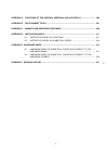
- i - contents chapter 1 general ......................................................................................................................... 1 1.1 function overview ......................................................................................... 2 1.2 ordering information .......
Page 10
- ii - chapter 3 features of the architecture and memory map ....................................... 21 3.1 data memory bank structure and addressing modes .................. 21 3.1.1 data memory bank structure .................................................................... 21 3.1.2 data memory...
Page 11
- iii - 5.3.5 operation of the watchdog timer ............................................................. 102 5.3.6 other functions ......................................................................................... 103 5.4 clock timer ...........................................................
Page 12
- iv - chapter 8 reset function ........................................................................................................... 225 chapter 9 writing to and verifying program memory (prom) ................................... 229 9.1 operating modes when writing to and verifying the progr...
Page 13
- v - appendix a functions of the µpd75008, µpd750008, and µpd75p0016 ............................ 299 appendix b development tools ................................................................................................ 301 appendix c masked rom ordering procedure .............................
Page 14
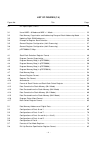
- vi - list of figures (1/4) figure no. Title page 2-1 pin input/output circuits .................................................................................................. 18 3-1 use of mbe = 0 mode and mbe = 1 mode ..................................................................... 22 3-2...
Page 15
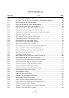
- vii - list of figures (2/4) figure no. Title page 5-9 i/o timing chart of digital i/o ports ................................................................................ 82 5-10 on timing chart of built-in pull-up resistor connected by software .......................... 83 5-11 block diagram o...
Page 16
- viii - list of figures (3/4) figure no. Title page 5-45 operations of relt and cmdt ....................................................................................... 141 5-46 transfer bit switching circuit .........................................................................................
Page 17
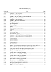
- ix - list of figures (4/4) figure no. Title page 5-81 format of the bit sequential buffer ................................................................................. 181 6-1 block diagram of interrupt control circuit ....................................................................... 184...
Page 18
- x - list of tables (1/2) table no. Title page 1-1 features of the products .................................................................................................. 1 2-1 digital i/o port pins ...................................................................................................
Page 19
- xi - list of tables (2/2) table no. Title page 7-1 operation statuses in the standby mode ........................................................................ 216 7-2 selection of a wait time with btm .................................................................................. 219 8-1 st...
Page 20
- xii - [memo].
Page 21
1 chapter 1 general chapter 1 general the µpd750004, µpd750006, µpd750008, and µpd75p0016 are 75xl series 4-bit single-chip microcom- puters. The 75xl series is a successor of the 75x series consisting of many products. These µpd750004, µpd750006, µpd750008, and µpd75p0016 are collectively called th...
Page 22
2 µpd750008 user's manual 1.1 function overview item function instruction execution • 0.95, 1.91, 3.81, 15.3 µs (when the main system clock operates at 4.19 mhz) time • 0.67, 1.33, 2.67, 10.7 µs (when the main system clock operates at 6.0 mhz) • 122 µs (when the subsystem clock operates at 32.768 kh...
Page 23
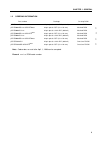
3 chapter 1 general 1.2 ordering information part number package on-chip rom µpd750004cu-xxx 42-pin plastic shrink dip (600 mil) masked rom µpd750004gb-xxx-3bs-mtx note 44-pin plastic qfp (10 x 10 mm) masked rom µpd750006cu-xxx 42-pin plastic shrink dip (600 mil) masked rom µpd750006gb-xxx-3bs-mtx n...
Page 24
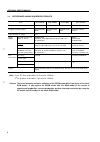
4 µpd750008 user's manual 1.3 differences among subseries products item µpd750004 µpd750006 µpd750008 µpd75p0016 program counter 12 bits 13 bits 14 bits program memory (byte) masked rom masked rom masked rom one-time prom 4096 6144 8192 16384 data memory (x 4 bits) 512 mask pull-up resistors at inco...
Page 25
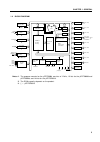
5 chapter 1 general 1.4 block diagram notes 1. The program counter for the µpd750004 consists of 12 bits, 13 bits for the µpd750006 and µpd750008, and 14 bits for the µpd75p0016. 2. The rom capacity depends on the product. 3. ( ) : µpd75p0016 ti0 pto0 pto1 buz si/sb1 so/sb0 sck int0 int1 int2 basic ...
Page 26
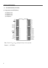
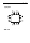
6 µpd750008 user's manual 1.5 pin configuration (top view) (1) 42-pin plastic shrink dip (600 mil) µpd750004cu-xxx µpd750006cu-xxx µpd750008cu-xxx µpd75p0016cu note connect ic (v pp ) to v dd , keeping the wiring as short as possible. Remark ( ) : µpd75p0016. Xt1 xt2 reset x1 x2 p33 (/md3) p32 (/md2...
Page 27
7 chapter 1 general (2) 44-pin plastic qfp (10 x 10 mm) µpd750004gb-xxx-3bs-mtx µpd750006gb-xxx-3bs-mtx µpd750008gb-xxx-3bs-mtx µpd75p0016gb-3bs-mtx note connect ic (v pp ) to v dd , keeping the wiring as short as possible. Remark ( ) : µpd75p0016. P72/kr6 p71/kr5 p70/kr4 p63/kr3 p62/kr2 p61/kr1 p60...
Page 28
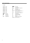
8 µpd750008 user's manual pin name p00-p03 : port 0 reset : reset input p10-p13 : port 1 ti0 : timer input 0 p20-p23 : port 2 pto0, 1 : programmable timer output 0, 1 p30-p33 : port 3 buz : buzzer clock p40-p43 : port 4 pcl : programmable clock p50-p53 : port 5 int0, 1, 4 : external vectored interru...
Page 29
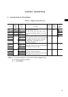
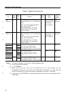
9 chapter 2 pin functions chapter 2 pin functions 2.1 pin functions of the µpd750008 table 2-1. Digital i/o port pins (1/2) input/ also 8 bit upon i/o pin used function circuit output as i/o reset type note 1 p00 input int4 4-bit input port (port0). X input b p01 i/o sck for p01 to p03, built-in pul...
Page 30
1 0 µpd750008 user's manual table 2-1. Digital i/o port pins (2/2) input also 8 bit upon i/o pin output used function circuit as i/o reset type note 1 p40- i/o — n-ch open-drain 4-bit i/o port (port4). O high level (when m-d p43 note 2, 4 withstand voltage is 13 v in open-drain a pull-up resistor (m...
Page 31
1 1 chapter 2 pin functions table 2-2. Non-port pin functions input/ also upon i/o pin output used function reset circuit as type note 1 ti0 input p13 inputs external event pulse to the timer/event counter — b -c pto0 i/o p20 timer/event counter output input e-b pto1 p21 timer counter output pcl i/o...
Page 32
1 2 µpd750008 user's manual 2.2 pin functions 2.2.1 p00-p03 (port0) : input pins used also for int4, sck, so/sb0 and si/sb1 p10-p13 (port1) : input pins used also for int0-int2, and ti0 these are the input pins of the 4-bit input ports: ports 0 and 1. Ports 0 and 1 function as input ports, and also ...
Page 33
1 3 chapter 2 pin functions 2.2.2 p20-p23 (port2) : i/o pins used also for pto0, pto1, pcl, and buz p30-p33 (port3) : i/o pins used also for md0-md3 note p40-p43 (port4), p50-p53 (port5) : n-ch open-drain intermediate withstand voltage (13 v) large-current output p60-p63 (port6), p70-p73 (port7) : t...
Page 34
1 4 µpd750008 user's manual 2.2.6 pcl: output pin used also for port 2 this is the programmable clock output pin. It is used to supply the clock pulse to a peripheral lsi circuit such as a slave microcomputer or a/d converter. A reset signal clears the clock mode register (clom) to 0, disabling cloc...
Page 35
1 5 chapter 2 pin functions int0 has a noise eliminator. Two different sampling clocks for noise elimination can be switched. The acceptable width of a signal depends on the cpu clock. Int1 is an asynchronous input, and can accept a signal with some high level width regardless of what the cpu clock ...
Page 36
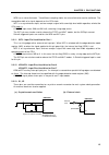
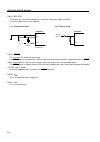
1 6 µpd750008 user's manual 2.2.14 xt1, xt2 these pins are used for connection to a crystal for subsystem clock oscillation. An external clock can also be applied. (a) crystal oscillation (b) external clock 2.2.15 reset this is the pin for active-low reset input. The reset input is asynchronous. Whe...
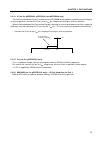
Page 37
1 7 chapter 2 pin functions 2.2.18 ic (for the µpd750004, µpd750006, and µpd750008 only) the internally connected (ic) pin is used to set the µpd750008 to test mode for inspection prior to shipping. In normal operation, connect the ic pin to the v dd pin, keeping the writing as short as possible. Wh...
Page 38
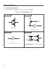
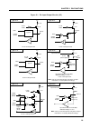
1 8 µpd750008 user's manual type b-c 2.3 pin input/output circuits figure 2-1 shows schematic diagrams of the i/o circuitry of the µpd750008. Figure 2-1. Pin input/output circuits (1/2) type a schmitt trigger input with hysteresis in cmos input buffer v dd in p-ch n-ch push-pull output which can be ...
Page 39
1 9 chapter 2 pin functions p.U.R.: pull-up resistor p.U.R. V dd p.U.R. Enable p-ch in/out data output disable type d type a type e-b type m-c figure 2-1. Pin input/output circuits (2/2) p.U.R.: pull-up resistor n-ch p.U.R. Data output disable p.U.R. Enable v dd p-ch in/out type f-a p.U.R.: pull-up ...
Page 40
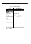
2 0 µpd750008 user's manual 2.4 connection of unused pins table 2-3. Connection of unused pins pin name recommended connection p00/int4 to be connected to v ss p01/sck to be connected to v ss or v dd p02/so/sb0 p03/si/sb1 p10/int0-p12/int2 to be connected to v ss p13/ti0 p20/pto0 input state: to be ...
Page 41
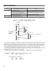
2 1 chapter 3 features of the architecture and memory map chapter 3 features of the architecture and memory map the 75xl series architecture of the µpd750008 has the following features: • internal ram of up to 4k words x 4 bits (12-bit address) • peripheral hardware expansibility to provide these fe...
Page 42
2 2 µpd750008 user's manual set1 mbe clr1 mbe set1 mbe mbe = 1 mbe = 0 meb = 1 clr1 mbe mbe = 0 ret ; mbe = 0 is to be set in the vector table. Mbe = 0 reti internal hardware and static ram operations are repeated. Applicable program processing effect mbe = 0 mode • interrupt processing mbs save/res...
Page 43
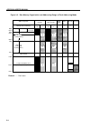
2 3 chapter 3 features of the architecture and memory map 3.1.2 data memory addressing modes with the architecture of the µpd750008, seven addressing modes summarized in figures 3-2 and 3-3, and table 3-1 are available to address data memory space efficiently for each bit length of data to be proces...
Page 44
2 4 µpd750008 user's manual figure 3-2. Data memory organization and addressing range of each addressing mode remark – : don't care addressing mode memory bank enable flag area for general register data area static ram (memory bank 0) data area static ram (memory bank 1) not provided peripheral hard...
Page 45
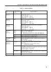
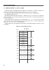
2 5 chapter 3 features of the architecture and memory map table 3-1. Addressing modes addressing mode representation specified address format 1-bit direct mem.Bit bit specified by bit at the address specified by mb and mem. Addressing • when mbe = 0 and mem = 00h-7fh, mb = 0 mem = 80h-ffh, mb = 15 •...
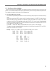
Page 46
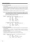
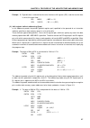
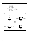
2 6 µpd750008 user's manual (2) 4-bit direct addressing (mem) in this addressing mode, the operand of an instruction directly specifies any area in the data memory space in units of four bits. As with the 1-bit direct addressing mode, in the mbe = 0 mode, a fixed space consisting of the static ram a...
Page 47
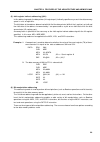
2 7 chapter 3 features of the architecture and memory map example 2. Eight-bit data is latched into the serial interface shift register (sio), and the transfer data is set at the same time. Sel mb15 ; mbs xch xa,sio ; xa (sio) (4) 4-bit register indirect addressing (@rpa) in this addressing mode, th...
Page 48
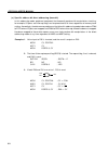
2 8 µpd750008 user's manual example 2. The data memory of 00h to ffh is cleared to 0. Clr1 rbe clr1 mbe mov xa,#00h mov hl,#04h loop: mov @hl,a ; (hl) incs hl ; hl br loop figure 3-3. Updating static ram addresses incs d decs d incs l decs l incs d decs d incs e decs e incs h decs h incs l decs l in...
Page 49
2 9 chapter 3 features of the architecture and memory map (5) 8-bit register indirect addressing (@hl) in this addressing mode, the data pointer (hl register pair) indirectly specifies any area in the data memory space in units of eight bits. The 4-bit data at the address determined with bit 0 of th...
Page 50
3 0 µpd750008 user's manual (a) specific address bit direct addressing (fmem.Bit) in this addressing mode, peripheral equipment that frequently performs bit manipulations involving, for example, i/o ports and interrupt flags, can be processed at all times regardless of memory bank setting. According...
Page 51
3 1 chapter 3 features of the architecture and memory map (b) specific address bit register indirect addressing (pmem.@l) in this addressing mode, the bits of peripheral hardware i/o ports are indirectly specified using a register to allow continuous manipulations. This addressing mode can be applie...
Page 52
3 2 µpd750008 user's manual (c) specific 1-bit direct addressing (@h+mem.Bit) this addressing mode enables any bit in the data memory space to be manipulated. In this addressing mode, the high-order four bits of the data memory address in the memory bank specified by mb = mbe·mbs are indirectly spec...
Page 53
3 3 chapter 3 features of the architecture and memory map (7) stack addressing this addressing mode is used for save/restoration operation in interrupt processing or subroutine processing. In this addressing mode, the address indicated by the stack pointer (8 bits) of data memory bank 0 is specified...
Page 54
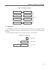
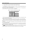
3 4 µpd750008 user's manual 3.2 general register bank configuration the µpd750008 contains four register banks, each consisting of eight general registers: x, a, b, c, d, e, h, and l. These registers are mapped to addresses 00h to 1fh in memory bank 0 of the data memory (see figure 3-5). To specify ...
Page 55
3 5 chapter 3 features of the architecture and memory map figure 3-4. Example of register bank selection the setting of the rbs can be modified for subroutine processing or interrupt processing by saving or restoring the rbs with the push or pop instruction. The rbe is set using the set1 or clr1 ins...
Page 56
3 6 µpd750008 user's manual (2) when used as an 8-bit register when the general register area is used on an 8-bit basis, the register pairs in the register bank specified by rbe·rbs can be specified as xa, bc, de, and hl as shown in figure 3-6, and the register pairs in the register bank that has th...
Page 57
3 7 chapter 3 features of the architecture and memory map figure 3-5. General register configuration (4-bit processing) x h d b x h d b x h d b x h d b 01h 03h 05h 07h 09h 0bh 0dh 0fh 11h 13h 15h 17h 19h 1bh 1dh 1fh a l e c a l e c a l e c a l e c 00h 02h 04h 06h 08h 0ah 0ch 0eh 10h 12h 14h 16h 18h ...
Page 58
3 8 µpd750008 user's manual figure 3-6. General register configuration (8-bit processing) xa hl de bc xa’ hl’ de’ bc’ 00h 02h 04h 06h 08h 0ah 0ch 0eh when rbe·rbs = 0 xa’ hl’ de’ bc’ xa hl de bc 00h 02h 04h 06h 08h 0ah 0ch 0eh when rbe·rbs = 1 xa hl de bc xa’ hl’ de’ bc’ 10h 12h 14h 16h 18h 1ah 1ch ...
Page 59
3 9 chapter 3 features of the architecture and memory map 3.3 memory-mapped i/o the µpd750008 employs memory-mapped i/o, which maps peripheral hardware such as timers and i/o ports to addresses f80h to fffh in data memory space as shown in figure 3-2. This means that there is no particular instructi...
Page 60
4 0 µpd750008 user's manual figure 3-7. µpd750008 i/o map (1/5) notes 1. Can be manipulated separately as the rbs and mbs in 4-bit units. Can also be manipulated as the bs in 8-bit units. Use sel mbn and sel rbn instructions to write data to mbs and rbs respectively. 2. Wdtm: watchdog timer enable f...
Page 61
4 1 chapter 3 features of the architecture and memory map figure 3-7. µpd750008 i/o map (2/5) notes 1. Toe0: timer/event counter output enable flag (w) 2. Toe1: timer counter output enable flag (w) fa0h fa2h fa4h fa6h fa8h fach address b3 b2 b1 b0 hardware name (symbol) r/ w 1 bit 4 bits 8 bits rema...
Page 62
4 2 µpd750008 user's manual figure 3-7. µpd750008 i/o map (3/5) remarks 1. Iexxx : interrupt enable flag 2. Irqxxx : interrupt request flag notes 1. Only bit 3 can be manipulated by an ei/di instruction. 2. Bits 3 and 2 can be manipulated bit by bit by a stop/halt instruction. (r/ w) fb0h fb2h fb3h ...
Page 63
4 3 chapter 3 features of the architecture and memory map figure 3-7. µpd750008 i/o map (4/5) note whether a bit can be read or written depends on the bit. Fd0h fdch fdeh address b3 b2 b1 b0 hardware name (symbol) r/ w 1 bit 4 bits 8 bits remarks number of bits that can be manipulated bit manipulati...
Page 64
4 4 µpd750008 user's manual figure 3-7. µpd750008 i/o map (5/5) notes 1. Bit 1 can be read or written only in serial operation enable mode. It can be read when four-bit manipulation is performed. 2. Kr0 to kr7 can be read (r) bit by bit. When inputting 4 bits at a time, specify port6 or port7. Ff0h ...
Page 65
4 5 chapter 4 internal cpu functions chapter 4 internal cpu functions 4.1 mk i mode/mk ii mode switch functions 4.1.1 differences between mk i mode and mk ii mode the cpu of the µpd750008 subseries has two modes (mk i mode and mk ii mode) and which mode is used is selectable. Bit 3 of the stack bank...
Page 66
4 6 µpd750008 user's manual 4.1.2 setting of the stack bank selection register (sbs) the mk i mode and mk ii mode are switched by stack bank selection register. Figure 4-1 shows the register configuration. The stack bank selection register is set with a 4-bit memory operation instruction. To use the...
Page 67
4 7 chapter 4 internal cpu functions pc12 pc11 pc10 pc9 pc8 pc7 pc6 pc5 pc4 pc3 pc2 pc1 pc0 pc13 pc10 pc9 pc8 pc7 pc6 pc5 pc4 pc3 pc2 pc1 pc0 pc11 pc11 pc10 pc9 pc8 pc7 pc6 pc5 pc4 pc3 pc2 pc1 pc0 pc12 4.2 program counter (pc): 12 bits (µpd750004) 13 bits (µpd750006 and µpd750008) 14 bits (µpd75p001...
Page 68
4 8 µpd750008 user's manual 4.3 program memory (rom): 4096 words x 8 bits (µpd750004: masked rom) 6144 words x 8 bits (µpd750006: masked rom) 8192 words x 8 bits (µpd750008: masked rom) 16384 words x 8 bits (µpd75p0016: one-time prom) the program memory is used for storing programs, an interrupt vec...
Page 69
4 9 chapter 4 internal cpu functions figure 4-3. Program memory map (in µpd750004) note can be used only in the mkii mode. Remark in addition to the above, the br pcde and br pcxa instructions can cause a branch to an address with only the 8 low-order bits of the pc changed. * mbe rbe 7 6 0000h mbe ...
Page 70
5 0 µpd750008 user's manual figure 4-4. Program memory map (in µpd750006) note can be used only in the mkii mode. Remark in addition to the above, the br pcde and br pcxa instructions can cause a branch to an address with only the 8 low-order bits of the pc changed. Mbe rbe 7 6 0000h mbe rbe 0002h m...
Page 71
5 1 chapter 4 internal cpu functions figure 4-5. Program memory map (in µpd750008) note can be used only in the mkii mode. Remark in addition to the above, the br pcde and br pcxa instructions can cause a branch to an address with only the 8 low-order bits of the pc changed. Mbe rbe 7 6 0000h mbe rb...
Page 72
5 2 µpd750008 user's manual figure 4-6. Program memory map (in µpd75p0016) note can be used only in the mkii mode. Remark in addition to the above, the br pcde and br pcxa instructions can cause a branch to an address with only the 8 low-order bits of the pc changed. * mbe rbe 7 6 0000h mbe rbe 0002...
Page 73
5 3 chapter 4 internal cpu functions 4.4 data memory (ram): 512 words x 4 bits the data memory consists of a data area and peripheral hardware area as shown in figure 4-7. The data memory consists of the following memory banks with each bank made of 256 words x 4 bits. • memory banks 0 and 1 (data a...
Page 74
5 4 µpd750008 user's manual 4.4.2 specification of a data memory bank if the memory bank enable flag (mbe) enables bank specification (mbe = 1), a memory bank is specified with the 4-bit memory bank select register (mbs = 0, 1, 15). If the mbe disables bank specification (mbe = 0), memory bank 0 or ...
Page 75
5 5 chapter 4 internal cpu functions data memory is undefined when it is reset. For this reason, it is to be initialized to zero (ram clear) usually at the start of a program. Remember to perform this initialization. Otherwise, unexpected bugs may occur. Example the following program clears data at ...
Page 76
5 6 µpd750008 user's manual 4.5 general register: 8 x 4 bits x 4 banks the general registers are mapped to particular addresses in data memory. Four banks of registers are provided, with each bank consisting of eight 4-bit registers (b, c, d, e, h, l, x, and a). The register bank (rb) to be enabled ...
Page 77
5 7 chapter 4 internal cpu functions figure 4-9. Register pair format 4.6 accumulator in the µpd750008, the a register and xa register pair function as accumulators. The a register is mainly used for 4-bit data processing instructions, and the xa register pair is mainly used for 8-bit data processin...
Page 78
5 8 µpd750008 user's manual 4.7 stack pointer (sp) and stack bank select register (sbs) the µpd750008 uses static ram as stack memory (lifo scheme), and the 8-bit register holding the start address of the stack area is the stack pointer (sp). The stack area is located at addresses 000h to 1ffh in me...
Page 79
5 9 chapter 4 internal cpu functions figure 4-11. Format of stack pointer and stack bank select register note the mk i mode and mk ii mode can be switched by bit 3 of sbs. The stack bank selection function can be used in both mk i mode and mk ii mode. (see section 4.1 for details.) example sp initia...
Page 80
6 0 µpd750008 user's manual pc11 - pc8 mbe sp + 2 pc3 - pc0 pc7 - pc4 sp + 4 ist1 cy sp + 6 sp + 1 sp + 3 sp + 5 stack rbe pc12 ist0 sk2 mbe sk1 rbe sk0 reti instruction psw pc11 - pc8 mbe sp + 2 pc3 - pc0 pc7 - pc4 sp + 4 sp + 1 sp + 3 stack rbe pc12 ret or rets instruction lower bits of pair regis...
Page 81
6 1 chapter 4 internal cpu functions figure 4-15. Data restored from the stack memory (mk ii mode) notes 1. Pc12 and pc13 are 0 in the µpd750004. Pc13 is 0 in the µpd750006 and µpd750008. 2. Psw bits other than mbe and rbe are not saved or restored. Remark * indicates an undefined bit. Lower bits of...
Page 82
6 2 µpd750008 user's manual 4.8 program status word (psw): 8 bits the program status word (psw) consists of various flags closely associated with processor operations. The psw is mapped to addresses fb0h and fb1h in data memory space. Four bits at address fb0h can be manipulated with a memory manipu...
Page 83
6 3 chapter 4 internal cpu functions table 4-4. Carry flag manipulation instructions instruction (mnemonic) carry flag operation/processing instruction dedicated to carry set1 cy sets cy to 1. Flag manipulation clr1 cy clears cy to 0. Not1 cy inverts the state of cy. Skt cy skips if cy is 1. Bit tra...
Page 84
6 4 µpd750008 user's manual table 4-5. Information indicated by the interrupt status flag ist1 ist0 status of processing processing and interrupt control being performed 0 0 status 0 normal program processing is being performed. Any interrupts are acceptable. 0 1 status 1 a lower- or higher-priority...
Page 85
6 5 chapter 4 internal cpu functions when the rbe is reset to 0, register bank 0 is always selected as general registers, regardless of the setting of the rbs. A reset signal automatically initializes the rbe by setting the rbe to the state of bit 6 at program memory address 0. When a vectored inter...
Page 86
6 6 µpd750008 user's manual table 4-6. Register bank to be selected with the rbe and rbs bank 0 is always selected. Rbe rbs 3 2 1 0 0 0 0 x x bank 0 is selected. 0 0 bank 1 is selected. 1 0 0 0 1 bank 2 is selected. 1 0 bank 3 is selected. 1 1 register bank x: don’t care always 0
Page 87
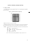
67 chapter 5 peripheral hardware functions chapter 5 peripheral hardware functions 5.1 digital i/o ports the µpd750008 employs the memory mapped i/o method. Thus, all input/output ports are mapped on the data memory space. Figure 5-1. Data memory addresses of digital ports remark some i/o parts can ...
Page 88
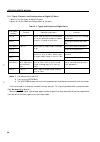
68 µpd750008 user's manual 5.1.1 types, features, and configurations of digital i/o ports table 5-1 lists the types of digital i/o ports. Figures 5-2 to 5-6 show the configurations of the ports. Table 5-1. Types and features of digital ports port name function operation and feature remarks (symbol) ...
Page 89
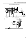
69 chapter 5 peripheral hardware functions figure 5-2. Configurations of ports 0 and 1 internal bus 8 csim selector selector p01 output latch internal sck si sck so int4 v dd pull-up resistor p-ch p00/int4 p01/sck p02/so/sb0 p03/si/sb1 bit 0 of poga input buffer output buffer which can be switched t...
Page 90
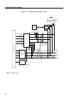
70 µpd750008 user's manual figure 5-3. Configurations of ports 2 and 7 note for port 7 only m p x input buffer pmm = 0 key interrupt note output latch pmm bits 2 and 7 of port mode register group b (m = 2, 7) output buffer internal bus pm0 pm1 pm2 pm3 bit m of poga pull-up resistor v dd p-ch input b...
Page 91
71 chapter 5 peripheral hardware functions figure 5-4. Configurations of ports 3n and 6n (n = 0 to 3) note for port 6n only bit m of poga pull-up resistor p-ch v dd pmn input buffer m p x pmmn = 0 pmmn = 1 pmmn output latch corresponding bits of port mode register group a output buffer m = 3, 6 n = ...
Page 92
72 µpd750008 user's manual figure 5-5. Configurations of ports 4 and 5 internal bus input buffer mpx v dd pm0 pm1 pm2 pm3 pmm = 0 pmm = 1 pmm output latch pull-up resistor n-ch open-drain output buffer corresponding bits of port mode register group b (m = 4, 5) (mask option).
Page 93
73 chapter 5 peripheral hardware functions figure 5-6. Configuration of port 8 internal bus p80 p81 bit 0 of pogb pull-up resistor v dd p-ch pm8 ouput latch m p x output buffer corresponding bit of port mode register group c input buffer pm8 = 1 pm8 = 0
Page 94
74 µpd750008 user's manual 5.1.2 i/o mode setting the i/o mode of each i/o port is set by the port mode register as shown in figure 5-7. The i/o modes of ports 3 and 6 can be set bit by bit by port mode register group a (pmga). The i/o modes of ports 2, 4, 5, and 7 can be set in units of four bits b...
Page 95
75 chapter 5 peripheral hardware functions figure 5-7. Formats of port mode registers 0 1 input mode (output buffer off) output mode (output buffer on) contents of specification pm63 pm62 pm61 pm60 pm33 pm31 pm32 pm30 7 6 5 4 3 1 2 0 fe8h address pmga symbol p30 i/o specification p31 i/o specificati...
Page 96
76 µpd750008 user's manual 5.1.3 digital i/o port manipulation instructions all i/o ports contained in the µpd750008 are mapped to data memory space, so that all data memory manipulation instructions can be used. Table 5-3 lists the instructions that are particularly useful for i/o pin manipulation ...
Page 97
77 chapter 5 peripheral hardware functions (3) 8-bit manipulation instructions the mov, xch, and ske instructions as well as the in and out instructions can be used for ports 4 and 5 that allow 8-bit manipulation. As with 4-bit manipulation, memory bank 15 must be selected in advance. Example the da...
Page 98
78 µpd750008 user's manual table 5-2. I/o pin manipulation instructions port port port port port port port port port port instruction 0 1 2 3 4 5 6 7 8 in a, portn note 1 in xa, portn note 1 — — — out portn, a note 1 — out portn, xa note 1 — — — set1 portn.Bit — set1 portn.@l note 2 — clr1 portn.Bit...
Page 99
79 chapter 5 peripheral hardware functions 5.1.4 digital i/o port operation when a data memory manipulation instruction is executed for a digital i/o port, the operation of the port and pins depends on the i/o mode setting (table 5-3). This is because data taken in on the internal bus is the data in...
Page 100
80 µpd750008 user's manual table 5-3. Operations by i/o port manipulation instructions instruction port and pin operation input mode output mode skt pin data is tested. Output latch data is tested. Skf mov1 cy, pin data is transferred to cy. Output latch data is transferred to cy. And1 cy, an operat...
Page 101
81 chapter 5 peripheral hardware functions 5.1.5 specification of bilt-in pull-up resistors a pull-up resistor can be contained at each port pin of the µpd750008 (except for p00). Whether to use the pull-up resistor can be specified by software (for some pins) or a mask option (for the other pins). ...
Page 102
82 µpd750008 user's manual figure 5-8. Pull-up resistor specification register format pull-up resistor specification register group a pull-up resistor specification register group b 5.1.6 i/o timing of digital i/o ports figure 5-9 shows the timing of data output to an output latch and the timing of ...
Page 103
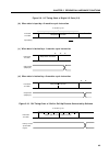
83 chapter 5 peripheral hardware functions figure 5-9. I/o timing chart of digital i/o ports (2/2) (b) when data is input by a 2-machine cycle instruction (c) when data is latched by a 1-machine cycle instruction (d) when data is latched by a 2-machine cycle instruction figure 5-10. On timing chart ...
Page 104
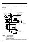
84 µpd750008 user's manual 5.2 clock generator the clock generator supplies various clock signals to the cpu and peripheral hardware to control the cpu operation mode. 5.2.1 clock generator configuration figure 5-11 shows the configuration of the clock generator. Figure 5-11. Block diagram of the cl...
Page 105
85 chapter 5 peripheral hardware functions 5.2.2 functions and operations of the clock generator the clock generator generates the following clocks, and controls the cpu operation modes such as the standby mode. • main system clock f x • subsystem clock f xt • cpu clock f • clock to peripheral hardw...
Page 106
86 µpd750008 user's manual (1) processor clock control register (pcc) the pcc is a 4-bit register for selecting a cpu clock f with the low-order two bits and for controlling the cpu operation mode with the high-order two bits (see figure 5-12). When bit 3 or bit 2 is set to 1, the standby mode is se...
Page 107
87 chapter 5 peripheral hardware functions figure 5-12. Format of the processor clock control register address fb3h 3 2 1 0 pcc3 pcc2 pcc1 pcc0 symbol pcc cpu clock selection bit (operation with f x = 6.0 mhz) ( ) is actual frequency at f x = 6.0 mhz cpu clock frequency Φ = f x /64 (93.7 khz) 1 mach...
Page 108
88 µpd750008 user's manual (2) system clock control register (scc) the scc is a 4-bit register for selecting cpu clock f with the least significant bit and for controlling the termination of main system clock generation with the most significant bit (see figure 5-13). Bits 0 and 3 of the scc are loc...
Page 109
89 chapter 5 peripheral hardware functions (3) system clock oscillator the main system clock oscillator operates with a crystal resonator or ceramic resonator connected to the x1 and x2 pins. An external clock can also be input. Input the clock signal to the x1 pin and the reversed signal to the x2 ...
Page 110
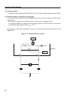
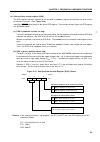
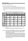
90 µpd750008 user's manual any line carrying a high pulsating current must be kept away as far as possible. • the grounding point of the capacitor of the oscillator must have the same potential as that of v ss . It must not be grounded to a grounding pattern carry ing a high current. • no signal mus...
Page 111
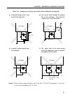
91 chapter 5 peripheral hardware functions figure 5-16. Examples of oscillator connections which should be avoided (2/2) (c) a high pulsating current is too (d) the current flows through the ground close to the signal line. Line of the oscillator. (the potential at points a, b, and c fluctuates.) (e...
Page 112
92 µpd750008 user's manual (4) frequency divider the frequency divider divides the output (f x ) of the main system clock oscillator to generate various clocks. (5) control functions of subsystem clock oscillator the subsystem clock oscillator of the µpd750008 subseries has two control functions to ...
Page 113
93 chapter 5 peripheral hardware functions (6) sub-oscillator control register (sos) the sos register specifies whether to use the built-in feedback register and controls the drive current of the built-in inverter. (see figure 5-18.) inputting a reset signal clears all bits of the sos register. The ...
Page 114
94 µpd750008 user's manual 5.2.3 system clock and cpu clock setting (1) time required to change the system clock and cpu clock the system clock and cpu clock can be changed by using the least significant bit of the scc and the low-order two bits of the pcc. This switching is not performed immediatel...
Page 115
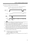
95 chapter 5 peripheral hardware functions (2) procedure for changing the system clock and cpu clock the procedure for changing the system clock and cpu clock is explained using figure 5-19. Figure 5-19. Changing the system clock and cpu clock a reset signal starts cpu operation at the lowest speed ...
Page 116
96 µpd750008 user's manual 5.2.4 clock output circuit (1) configuration of the clock output circuit figure 5-20 shows the configuration of the clock output circuit. (2) functions of the clock output circuit the clock output circuit outputs a clock pulse signal on the p22/pcl pin to output remote con...
Page 117
97 chapter 5 peripheral hardware functions (3) clock output mode register (clom) the clom is a 4-bit register to control clock output. The clom is set by a 4-bit memory manipulation instruction. No read operation is allowed on this register. Example cpu clock f is output on the pcl/p22 pin. Sel mb15...
Page 118
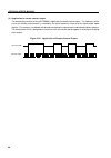
98 µpd750008 user's manual (4) application to remote control output the clock output function of the µpd750008 is applicable to remote control output. The frequency of the carrier for remote control output is selected by the clock frequency select bit of the clock output mode register. Pulse output ...
Page 119
99 chapter 5 peripheral hardware functions 5.3 basic interval timer/watchdog timer the µpd750008 contains an 8-bit basic interval timer/watchdog timer, which has the following functions: (a) interval timer operation which generates a reference timer interrupt (b) operation as a watchdog timer for de...
Page 120
100 µpd750008 user's manual when bit 3 is set to 1, the bt is cleared, and the basic interval ltimer/watchdog timer interrupt request flag (irqbt) is also cleared (to start the basic interval timer/watchdog timer). A reset signal clears the interval timer to 0, and the longest interrupt request sign...
Page 121
101 chapter 5 peripheral hardware functions 5.3.3 watchdog timer enable flag (wdtm) wdtm, when set, is a flag for enabling the generation of the reset signal when the basic interval timer overflows. Wdtm is set by a bit manipulation instruction. It cannot be cleared by an instruction. Example set th...
Page 122
102 µpd750008 user's manual 5.3.5 operation of the watchdog timer when wdtm is set to 1, the basic interval timer/watchdog timer functions as a watchdog timer. An internal reset signal is generated when the basic interval timer (bt) overflows. No reset signal, however, is generated during the oscill...
Page 123
103 chapter 5 peripheral hardware functions ······ module 1: set1 sel set1 mbe mb15 btm.3 processing completes within 5.46 ms. ······ module 2: set1 sel set1 mbe mb15 btm.3 processing completes within 5.46 ms. ··· 5.3.6 other functions the basic interval timer/watchdog has the following functions re...
Page 124
104 µpd750008 user's manual (2) reading the count the count status of the basic interval timer (bt) can be read by using an 8-bit manipulation instruction. No data can be loaded to the timer. Caution when reading the count value of bt, execute a read instruction twice so that unstable data which has...
Page 125
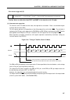
105 chapter 5 peripheral hardware functions mov xa, bc mov buff, xa ; store data set1 flag ; set data presence flag reti 5.4 clock timer the µpd750008 contains one clock timer, which has the following functions. (a) the clock timer sets the test flag (irqw) every 0.5 seconds. The irqw can release th...
Page 126
106 µpd750008 user's manual 5.4.1 configuration of the clock timer figure 5-26 shows the configuration of the clock timer. Figure 5-26. Block diagram of the clock timer the values in parentheses are for f x = 4.194304 mhz and f xt = 32.768 khz. 5.4.2 clock mode register the clock mode register (wm) ...
Page 127
107 chapter 5 peripheral hardware functions example time is set using the main system clock (4.19 mhz), and buzzer output is enabled: clr1 mbe mov xa, #84h mov wm, xa ; sets wm figure 5-27. Clock mode register format remark ( ) for f w = 32.768 khz address f98h symbol wm 0 wm0 1 wm1 2 wm2 3 wm3 4 wm...
Page 128
108 µpd750008 user's manual 5.5 timer/event counter the µpd750008 has one timer/event counter channel (channel 0) and one timer counter channel (channel 1). Figures 5-28 and 5-29 show the configuration of these channels. In this section, the timer/event counter and timer counters are referred to as ...
Page 129
109 chapter 5 peripheral hardware functions figure 5-28. Block diagram of the timer/event counter (channel 0) count register (8) ti0 mpx timer operation start signal 8 8 8 from the clock generator internal bus tm06 tm05 tm04 tm03 tm02 port input buffer comparator (8) modulo register (8) to enable fl...
Page 130
110 µpd750008 user's manual figure 5-29. Block diagram of the timer counter (channel 1) count register (8) mpx timer operation start signal 8 8 8 from the clock generator internal bus tm16 tm15 tm14 tm13 tm12 comparator (8) modulo register (8) to enable flag p21 output latch signal port 2 input/ out...
Page 131
111 chapter 5 peripheral hardware functions (1) timer/event counter mode register (tm0, tm1) the mode register (tmn) is an 8-bit register which controls the timer/event counter. Its format is shown in figures 5-30 and 5-31. The timer/event counter mode register is set by an 8-bit memory manipulation...
Page 132
112 µpd750008 user's manual figure 5-30. Timer/event counter mode register (channel 0) format when f x = 4.19 mhz tm05 0 0 0 0 1 1 tm06 0 0 1 1 1 1 tm04 0 1 0 1 0 1 ti0 rising edge ti0 falling edge f x /2 10 (4.09 khz) f x /2 8 (16.4 khz) f x /2 6 (65.5 khz) f x /2 4 (262 khz) not to be set count pu...
Page 133
113 chapter 5 peripheral hardware functions figure 5-31. Timer counter mode register (channel 1) format address fa8h 7 6 tm16 5 tm15 4 tm14 3 tm13 2 tm12 1 0 symbol tm1 tm13 timer start indication bit when 1 is written into the bit, the counter and irqt1 flag are cleared. If bit 2 is set to 1, count...
Page 134
114 µpd750008 user's manual (2) timer/event counter output enable flag (toe0, toe1) the timer/event counter output enable flag (toe0, toe1) controls the output enable/disable to the pto0 and pto1 pins in the timer out flip-flop (tout flip-flop ) status. The timer out flip-flop is inverted by the mat...
Page 135
115 chapter 5 peripheral hardware functions figure 5-33. Timer/event counter mode register setup (1/2) (a) in the case of timer/event counter (channel 0) timer start indication bit when “1” is written into the bit, the counter and irqt0 flag are cleared. If bit 2 is set to “1”, count operation is st...
Page 136
116 µpd750008 user's manual figure 5-33. Timer/event counter mode register setup (2/2) (b) in the case of timer counter (channel 1) (b) timer/event counter output enable flag (toen) the toen is manipulated by a bit manipulation instruction. The toen is cleared to 0 by an internal reset signal. Figur...
Page 137
117 chapter 5 peripheral hardware functions (2) timer/event counter time setting [timer setup time] (cycle) is found by dividing [modulo register contents + 1] by [count pulse (cp) frequency] selected by setting the mode register. N+1 t (sec) = = (n + 1) · (resolution) f cp t (sec) : timer setup tim...
Page 138
118 µpd750008 user's manual (3) timer/event counter operation the timer/event counter operates as follows. Figure 5-35 shows the configuration of the timer/event counter. The count pulse (cp) is selected by setting the mode register (tmn) and is input to the count register (tn). The tn is compared w...
Page 139
119 chapter 5 peripheral hardware functions figure 5-36. Count operation timing (4) applications of the timer/event counter (a) timer/event counter is used as an interval timer that generates interrupts at intervals of 30 ms. • the high-order four bits of the mode register are set to 0100b to select...
Page 140
120 µpd750008 user's manual sel mb15 mov xa,#100 – 1 mov tmod0,xa ; set the modulo register mov xa,#00001100b mov tm0,xa ; set the mode register ei ei iet0 ; enable intt0 5.5.3 notes on timer/event counter applications (1) time error at the start of the timer a maximum error of one count pulse (cp) ...
Page 141
121 chapter 5 peripheral hardware functions (3) error in reading the count register the contents of the count register can be read using an 8-bit data memory manipulation instruction at any time. During operation by such an instruction, all count pulse changes are held not to change the count regist...
Page 142
122 µpd750008 user's manual (5) operation after the modulo register is changed the contents of the modulo register are changed when an 8-bit data memory manipulation instruction is executed. If the new value of the modulo register is less than the value of the count register, the count register cont...
Page 143
123 chapter 5 peripheral hardware functions 5.6 serial interface 5.6.1 serial interface functions the µpd750008 contains a clock synchronous 8-bit serial interface, which has four modes. The functions of the four modes are outlined below. (1) operation halt mode this mode is used when serial transfe...
Page 144
124 µpd750008 user's manual figure 5-38. Example of the sbi system configuration 5.6.2 configuration of serial interface figure 5-39 shows the block diagram of the serial interface. Sck master cpu sb0, sb1 sck sb0, sb1 slave cpu #1 address 1 sck sb0, sb1 slave ic #n address n address command data se...
Page 145
125 chapter 5 peripheral hardware functions figure 5-39. Block diagram of the serial interface internal bus 8 8 8 8/4 p03/si0/sb1 p02/so0/sb0 p01/sck (8) f x /2 3 f x /2 4 f x /2 6 tout0 (from timer/event counter) csim reld cmdd ackd ackt acke bsye relt cmdt dq set clr (8) (8) sbic bit test slave ad...
Page 146
126 µpd750008 user's manual (1) serial operation mode register 0 (csim) csim is an 8-bit register which specifies a serial interface operation mode, serial clock, wake-up function, and so forth. (see (1) in section 5.6.3 for details.) (2) serial bus interface control register (sbic) sbic is an 8-bit...
Page 147
127 chapter 5 peripheral hardware functions (9) serial clock control circuit the serial clock control circuit controls the serial clock to be supplied to the shift register, or controls the clock to be output to the sck pin when the internal system clock is used. (10) busy/acknowledge output circuit...
Page 148
128 µpd750008 user's manual figure 5-40. Format of serial operation mode register (csim) (2/4) serial interface operation enable/disable specification bit (w) shift register serial clock irqcsi so/sb0 and operation counter flag si/sb1 pins csie 0 shift operation cleared held used only for port 0 dis...
Page 149
129 chapter 5 peripheral hardware functions figure 5-40. Format of serial operation mode register (csim) (3/4) serial interface operation mode selection bit (w) csim4 csim3 csim2 operation bit order of so pin si pin mode shift register function function x 0 0 3-wire sio 7-0 xa so/p02 si/p03 serial (...
Page 150
130 µpd750008 user's manual figure 5-40. Format of serial operation mode register (csim) (4/4) remarks 2. The p01/sck pin assumes any of the following states according to the state of csie, csim1, and csim0: csie csim1 csim0 p01/sck pin state 0 0 0 input port 1 0 0 high impedance 0 0 1 high level ou...
Page 151
131 chapter 5 peripheral hardware functions (2) serial bus interface control register (sbic) figure 5-41 shows the format of the serial bus interface control register (sbic). Sbic is an 8-bit register consisting of bits for controlling the serial bus and flags for indicating the states of input data...
Page 152
132 µpd750008 user's manual figure 5-41. Format of serial bus interface control register (sbic) (2/3) busy enable bit (r/w) bsye 0 the busy signal is automatically disabled. Busy signal output is stopped in phase with the falling edge of sck immediately after clear instruction execution. 1 the busy ...
Page 153
133 chapter 5 peripheral hardware functions figure 5-41. Format of serial bus interface control register (sbic) (3/3) bus release detection flag (r) reld condition for being cleared (reld = 0) condition for being set (reld = 1) the transfer start instruction is executed. The bus release signal (rel)...
Page 154
134 µpd750008 user's manual (3) shift register (sio) figure 5-42 shows the configuration of peripheral hardware of shift register. Sio is an 8-bit register which performs parallel-serial conversion and serial transfer (shift) operation in phase with the serial clock. Serial transfer is started by wr...
Page 155
135 chapter 5 peripheral hardware functions (a) slave address detection [in the sbi mode] sva is used when the µpd750008 is connected as a slave device to the serial bus. Sva is an 8- bit register for a slave to set its slave address (number assigned to it). The master outputs a slave address to the...
Page 156
136 µpd750008 user's manual note the status of the p01/sck pin is selectable. Remark (r): read only (w): write only serial interface operation enable/disable specification bit (w) shift register operation serial clock counter irqcsi flag so/sb0 and si/sb1 pins csie0 0 shift operation disabled cleare...
Page 157
137 chapter 5 peripheral hardware functions 5.6.5 three-wire serial i/o mode operations the three-wire serial i/o mode is compatible with other modes used in the 75 xl series, 75x series, µpd7500 series, and 87ad series. Communication is performed using three lines: serial clock (sck), serial output...
Page 158
138 µpd750008 user's manual serial interface operation enable/disable specification bit (w) shift register operation serial clock counter irqcsi flag so/sb0 and si/sb1 pins csie 1 shift operation enabled count operation can be set used in each mode as well as for port 0 signal from address comparato...
Page 159
139 chapter 5 peripheral hardware functions (b) serial bus interface control register (sbic) to use the three-wire serial i/o mode, set sbic as shown below. (for details on sbic format, see (2) in section 5.6.3.) sbic is manipulated using a bit memory manipulation instruction. When the reset signal ...
Page 160
140 µpd750008 user's manual sck si irqcsi 1 so 2 3 4 5 6 7 8 di0 do0 di1 do1 di2 do2 di3 do3 di4 do4 di5 do5 di6 do6 di7 do7 transfer operation is started in phase with falling edge of sck. Execution of instruction that writes data to sio (transfer start request) completion of transfer figure 5-44. ...
Page 161
141 chapter 5 peripheral hardware functions (4) signals figure 5-45 shows operations of relt and cmdt. Figure 5-45. Operations of relt and cmdt (5) switching between msb and lsb as the first transfer bit the three-wire serial i/o mode has a function that can switch between the msb and lsb as the fir...
Page 162
142 µpd750008 user's manual (6) transfer start serial transfer is started by writing transfer data into shift register (sio), provided that the following two conditions are satisfied: • the serial interface operation enable/disable specification bit (csie) is set to 1. • the internal serial clock is...
Page 163
143 chapter 5 peripheral hardware functions (b) data is transmitted and received starting with the lsb on an external clock (slave operation). (in this case, the function of inverting the msb/lsb is used for shift register read/write operation.) main routine clr1 mbe mov xa,#84h mov csim,xa ; serial...
Page 164
144 µpd750008 user's manual sck master cpu (µpd750008) sb0, sb1 slave cpu sck sb0, sb1 v dd 2-wire serial i/o 2-wire serial i/o (master side): clr1 mbe mov xa,#10000011b mov csim,xa ; set transfer mode mov xa,tdata mov sio,xa ; set transfer data, and start transfer . . . . . . . . . . Loop : sktclr ...
Page 165
145 chapter 5 peripheral hardware functions (a) serial operation mode register (csim) to use the two-wire serial i/o mode, set csim as shown below. (for details on csim format, see (1) in section 5.6.3.) csim is manipulated using an 8-bit manipulation instruction. Bits 7, 6, and 5 of csim can be man...
Page 166
146 µpd750008 user's manual serial interface operation mode selection bit (w) csim4 csim3 csim2 shift register sequence so pin function si pin function 0 1 1 sio 7-0 xa sb0/p02 (n-ch p03 input (transfer starting with msb) open-drain i/o) 1 p02 input sb1/p03 (n-ch open-drain i/o) serial clock selecti...
Page 167
147 chapter 5 peripheral hardware functions bus release trigger bit (w) relt control bit for bus release signal (rel) trigger output. By setting relt = 1, the so latch is set to 1. Then the relt bit automatically cleared to 0. Caution never use bits other than relt and cmdt in the two-wire serial i/...
Page 168
148 µpd750008 user's manual (3) serial clock selection to select the serial clock, manipulate bits 0 and 1 of serial operation mode register (csim). The serial clock can be selected out of the following four clocks: table 5-8. Serial clock selection and application (in the two-wire serial i/o mode) ...
Page 169
149 chapter 5 peripheral hardware functions (6) error detection in the two-wire serial i/o mode, the state of serial bus sb0 or sb1 being used for communication is loaded into the shift register (sio) of the transmitting device. So a transmission error can be detected by the methods described below....
Page 170
150 µpd750008 user's manual the µpd750008, which is the master microcomputer, outputs a serial clock, and all slave microcomputers operate with an external clock. 5.6.7 sbi mode operation the sbi (serial bus interface) is a high-speed serial interface that conforms to the nec serial bus format. To a...
Page 171
151 chapter 5 peripheral hardware functions cautions 1. In the sbi mode, the serial data bus pin sb0 (or sb1) is an open-drain output. So the serial data bus line is placed in the wired or state. A pull-up resistor is required for the serial data bus line. 2. To switch between the master and slave, ...
Page 172
152 µpd750008 user's manual (2) sbi definition the format of serial data and signal used in the sbi mode are described below. Serial data to be transferred in the sbi mode is classified into three types: address, command, and data. Serial data forms one frame as shown below. Figure 5-51 is a timing ...
Page 173
153 chapter 5 peripheral hardware functions (a) bus release signal (rel) when the sck line is high (the serial clock is not output), the sb0 (or sb1) line changes from low to high. This signal is called the bus release signal, and is output by the master. Figure 5-52. Bus release signal this signal ...
Page 174
154 µpd750008 user's manual figure 5-55. Slave selection using an address (d) command and data the master sends commands to the slave selected by sending an address. The master also transfers data to or from the slave. Figure 5-56. Command figure 5-57. Data the 8-bit data following the command signa...
Page 175
155 chapter 5 peripheral hardware functions figure 5-58. Acknowledge signal [when output in phase with the 11th clock of sck] [when output in phase with the 9th clock of sck] the acknowledge signal is a one-shot pulse output in phase with the falling edge of sck after 8-bit data transfer. This signa...
Page 176
156 µpd750008 user's manual sb0, sb1 8 9 ack busy ready sck (f) busy signal (busy) and ready signal (ready) the busy signal informs the master that a slave is getting ready for data transfer. The ready signal informs the master that a slave is ready for data transfer. Figure 5-59. Busy and ready sig...
Page 177
157 chapter 5 peripheral hardware functions serial interface operation enable/disable specification bit (w) shift register operation serial clock counter irqcsi flag so/sb0 and si/sb1 pins csie 1 shift operation enabled count operation can be set used in each mode as well as for port 0 signal from a...
Page 178
158 µpd750008 user's manual serial clock selection bit (w) csim1 csim0 serial clock sck pin mode 0 0 external clock applied to sck pin input 0 1 timer/event counter output (tout0) output 1 0 f x /2 4 (262 khz) 1 1 f x /2 3 (524 khz) remark the value at 4.19 mhz is indicated in parentheses. (b) seria...
Page 179
159 chapter 5 peripheral hardware functions acknowledge detection flag (r) ackd condition for being cleared (ackd = 0) condition for being set (ackd = 1) the transfer operation is started. The acknowledge signal (ack) is detected the reset signal is entered. (in phase with the rising edge of sck). A...
Page 180
160 µpd750008 user's manual bus release trigger bit (w) relt control bit for bus release signal (rel) trigger output. By setting relt = 1, the so latch is set to 1. Then the relt bit automatically cleared to 0. Caution never clear sb0 (or sb1) during serial transfer. Be sure to clear sb0 (or sb1) be...
Page 181
161 chapter 5 peripheral hardware functions figure 5-60. Operations of relt, cmdt, reld, and cmdd (master) figure 5-61. Operations of relt, cmdt, reld, and cmdd (slave) sio sck so latch relt cmdt reld cmdd transfer start request "h" sio sck 1 2 7 8 d7 d6 d1 d0 so latch relt (master) cmdt (master) re...
Page 182
162 µpd750008 user's manual figure 5-62. Operation of ackt caution do not set the ackt until the transfer is completed. Figure 5-63. Operation of acke (1/2) (a) when acke = 1 at time of transfer completion (b) when acke is set after transfer completion (c) when acke = 0 at time of transfer completio...
Page 183
163 chapter 5 peripheral hardware functions sio sck 9 8 d2 d1 d0 sb0, sb1 ackd 7 6 ack transfer start request transfer start figure 5-63. Operation of acke (2/2) (d) when acke = 1 period is too short figure 5-64. Operation of ackd (1/2) (a) when ack signal is output during the ninth sck clock (b) wh...
Page 184
164 µpd750008 user's manual figure 5-64. Operation of ackd (2/2) (c) clear timing for case where start of transfer is directed during busy figure 5-65. Operation of bsye sck sb0, sb1 bsye 9 busy 8 7 6 ack when bsye = 1 at this point when reset operation is executed during this period and bsye = 0 at...
Page 185
165 chapter 5 peripheral hardware functions table 5-10. Various signals used in the sbi mode (1/2) sck sb0, sb1 “h” “h” sck sb0, sb1 rising edge of sb0 or sb1 when sck = 1 falling edge of sb0 or sb1 when sck = 1 low level signal output on sb0 or sb1 during one sck clock cycle after serial reception ...
Page 186
166 µpd750008 user's manual table 5-10. Various signals used in the sbi mode (2/2) synchronous clock for outputting address / command/data, ack signal, synchronous busy signal, and so on. Address/command/data is output during first 8 clock cycles. 8-bit data transferred in phase with sck after rel s...
Page 187
167 chapter 5 peripheral hardware functions (6) pin configuration the configurations of serial clock pin sck and serial data bus pin (sb0 or sb1) are as follows: (a) sck: pin for serial clock i/o master : cmos, push-pull output slave : schmitt input (b) sb0, sb1: pin for serial data i/o output to sb...
Page 188
168 µpd750008 user's manual (7) address match detection method in the sbi mode, communication starts when the master selects a particular slave device by outputting an address. An address match is detected by hardware. The slave address register (sva) is available. In the wake- up state (wup = 1), i...
Page 189
169 chapter 5 peripheral hardware functions figure 5-67. Address transfer operation from master device to slave device (wup = 1) program processing hardware operation program processing sck pin 12 345 6 78 9 sb0 or sb1 pin a7 hardware operation a6 a5 a4 a3 a2 a1 a0 ack ready address master device pr...
Page 190
170 µpd750008 user's manual figure 5-68. Command transfer operation from master device to slave device program processing hardware operation program processing sck pin 12 345 6 78 9 sb0 or sb1 pin c7 hardware operation c6 c5 c4 c3 c2 c1 c0 ack ready command master device processing (transmitter) tra...
Page 191
171 chapter 5 peripheral hardware functions figure 5-69. Data transfer operation from master device to slave device program processing hardware operation program processing sck pin 12 345 6 78 9 sb0 or sb1 pin d7 hardware operation d6 d5 d4 d3 d2 d1 d0 ack ready data master device processing (transm...
Page 192
172 µpd750008 user's manual figure 5-70. Data transfer operation from slave device to master device program processing hardware operation program processing sck pin 12 345 6 78 9 1 2 sb0 or sb1 pin busy ready d7 hardware operation d6 d5 d4 d3 d2 d1 d0 ack busy d7 d6 ready data master device processi...
Page 193
173 chapter 5 peripheral hardware functions (10) transfer start serial transfer is started by writing transfer data in shift register (sio), provided that the following two conditions are satisfied: • the serial interface operation enable/disable bit (csie) is set to 1. • the internal serial clock i...
Page 194
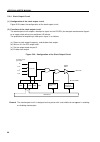
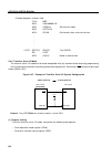
174 µpd750008 user's manual (12) sbi mode this section describes an example of application which performs serial data communication in the sbi mode. In the example, the µpd750008 can be used as either the master cpu or a slave cpu on the serial bus. The master can be switched to another cpu with a c...
Page 195
175 chapter 5 peripheral hardware functions (b) explanation of commands (i) types of commands this example uses the following commands: read command : transfers data from slave to master. Write command : transfers data from master to slave. End command : informs slave of write command completion. St...
Page 196
176 µpd750008 user's manual when the slave receives a transmission data count, if it has data enough for transmitting the specified number of bytes of data, the slave returns ack. If the slave does not have enough data for transmission, an error occurs; ack is not returned in this case. The master s...
Page 197
177 chapter 5 peripheral hardware functions status command the status command reads the status of the current slave. Figure 5-75. Transfer format of the status command remark m: output by the master s: output by the slave the slave returns the status in the format shown in figure 5-78. Figure 5-76. ...
Page 198
178 µpd750008 user's manual reset command the reset command changes the currently selected slave to a non-selected slave. When a reset command is transmitted, any slave can be placed in the non-selected state. Figure 5-77. Transfer format of the reset command remark m: output by the master s: output...
Page 199
179 chapter 5 peripheral hardware functions if ack is not returned from the slave within a predetermined period after transmission completion, the occurrence of an error is assumed; the master outputs the ack signal as a dummy. Figure 5-79. Master and slave operation in case of error the following e...
Page 200
180 µpd750008 user's manual p01/sck p01 output latch sck to internal circuit address ff0h.1 sck pin output mode from the serial clock control circuit example to output one sck/p01 pin clock cycle by software sel mb15 ; or clr1 mbe mov xa,#10000011b ; sck (f x /2 3 ), output mode mov csim,xa clr1 0ff...
Page 201
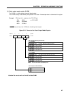
181 chapter 5 peripheral hardware functions 5.7 bit sequential buffer: 16-bit the bit sequential buffer (bsb) is special data memory for bit manipulations. In particular, the buffer allows bit manipulations to be performed very easily by sequentially changing address and bit specifications. So the b...
Page 202
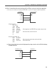
182 µpd750008 user's manual example to output 16-bit data of buff1 and buff2 serially from bit 0 of port 3: clr1 mbe mov xa,buff1 mov bsb0,xa ; set bsb0 and bsb1 mov xa,buff2 mov bsb2,xa ; set bsb2 and bsb3 mov l,#0 loop0: skt bsb0, @l ; tests the specification bit of bsb br loop1 nop ; dummy (for t...
Page 203
183 chapter 6 interrupt and test functions chapter 6 interrupt and test functions the µpd750008 has seven vectored interrupt sources and two test inputs, allowing a wide range of applications. In addition, the interrupt control circuitry of the µpd750008 has the following features for very high-spee...
Page 204
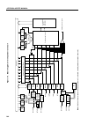
184 µpd750008 user's manual figure 6-1. Block diagram of interrupt control circuit* 2 im2 14 irqbt irq4 irq0 irq1 irqcsi irqt0 irqt1 irqw irq2 intbt int4/p00 int0/p10 int1/p11 intcsi intt0 intt1 intw int2/p12 both-edge detection circuit im0 edge detection circuit edge detection circuit rising edge d...
Page 205
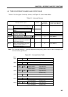
185 chapter 6 interrupt and test functions 6.2 types of interrupt sources and vector tables table 6-1 lists the types of interrupt sources, and figure 6-2 shows vector tables. Table 6-1. Interrupt sources interrupt source signal in/out interrupt vectored interrupt request priority note (vector table...
Page 206
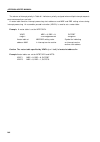
186 µpd750008 user's manual the column of interrupt priority in table 6-1 indicates a priority assigned when multiple interrupt requests occur concurrently or are held. A vector table contains interrupt processing start addresses and mbe and rbe setting values during interrupt processing. An assembl...
Page 207
187 chapter 6 interrupt and test functions 6.3 various devices to control interrupt functions (1) interrupt request flags and interrupt enable flags the following seven interrupt request flags (irqxxx) corresponding to the interrupt sources are provided. Int0 interrupt request flag (irq0) serial int...
Page 208
188 µpd750008 user's manual table 6-2. Set signals for interrupt request flags interrupt set signals for interrupt request flags interrupt request flag enable flag irqbt set by a reference time interval signal from the basic interval timer/watchdog iebt timer. Irq4 set by a detected rising or fallin...
Page 209
189 chapter 6 interrupt and test functions figure 6-3. Interrupt priority specification register ips0 ips1 ips2 ips3 0 1 2 3 ips symbol fb2h address 0 0 0 0 0 1 0 1 0 0 1 1 1 0 0 1 0 1 1 1 0 1 1 1 0 1 high-order interrupt selection all low-order interrupt vrq1 (intbt/int4) vrq2 (int0) vrq3 (int1) vr...
Page 210
190 µpd750008 user's manual (3) configurations of the int0, int1, and int4 circuits (a) as shown in figure 6-4 (a), the int0 circuit accepts an external interrupt at its rising or falling edge. The edge to be detected can be selected. The int0 circuit has a noise elimination function (see figure 6-5...
Page 211
191 chapter 6 interrupt and test functions figure 6-4. Configurations of the int0, int1, and int4 circuits (a) configuration of the int0 circuit (b) configuration of the int1 circuit (c) configuration of the int4 circuit int0/p10 im00, im01 internal bus im0 4 edge detection circuit irq0 set signal i...
Page 212
192 µpd750008 user's manual figure 6-5. I/o timing of a noise eliminator remark t smp = t cy or 64/f x int0 shaped output int0 int0 int0 shaped output shaped output shaped output shorter than sampling cycle (t smp ) 1 to 2 times longer than 2 times (a) (b) t smp t smp t smp t smp t smp l l h h l l h...
Page 213
193 chapter 6 interrupt and test functions figure 6-6. Format of edge detection mode registers (a) int0 edge detection mode register (im0) (b) int1 edge detection mode register (im1) caution changing the edge detection mode register may set an interrupt request flag. So, disable the interrupts befor...
Page 214
194 µpd750008 user's manual (4) interrupt status flags the interrupt status flags (ist0 and ist1), which are contained in the psw, indicate the status of processing currently executed by the cpu. By using the content of these flags, the interrupt priority control circuit controls multiple interrupts...
Page 215
195 chapter 6 interrupt and test functions 6.4 interrupt sequence when an interrupt occurs, it is processed using the procedure shown in figure 6-7. Figure 6-7. Interrupt sequence notes 1. Ist0 and ist1 are the interrupt status flags (bits 3 and 2 of the psw). (see table 6-3.) 2. An interrupt servic...
Page 216
196 µpd750008 user's manual 6.5 multiple interrupt processing control the µpd750008 can handle multiple interrupts by either of the following methods. (1) multiple interrupt processing by a high-order interrupt in this method, the µpd750008 selects an interrupt source among multiple interrupt source...
Page 217
197 chapter 6 interrupt and test functions (2) multiple interrupt processing by changing the interrupt status flags changing the interrupt status flags with the program causes multiple interrupts to be enabled. That is, when the interrupt processing program changes both ist1 and ist0 to 0 (status 0)...
Page 218
198 µpd750008 user's manual 6.6 processing of interrupts sharing a vector address interrupt sources intbt and int4 share a vector table, so an interrupt source is selected as described below. (1) using only one interrupt the interrupt enable flag for desired one of the two interrupt sources sharing ...
Page 219
199 chapter 6 interrupt and test functions examples 1. To use both intbt and int4 as having the higher priority and give priority to int4 di sktclr irq4 ; irq4 = 1 ? Br vsubbt processing routine ei of int4 reti vsubbt: clr1 irqbt processing routine of intbt ei reti 2. To use both intbt and int4 as h...
Page 220
200 µpd750008 user's manual 6.7 machine cycles for starting interrupt processing with the µpd750008 series, the following machine cycles are used to start the execution of the interrupt service routine after an interrupt request flag (irqn) is set. (1) when irqn is set during execution of an interru...
Page 221
201 chapter 6 interrupt and test functions (2) when irqn is set during an instruction other than that described in (1) (a) when irqn is set at the last machine cycle of the instruction being executed in this case, an instruction preceded by the instruction being executed is executed, and an interrup...
Page 222
202 µpd750008 user's manual 6.8 effective use of interrupts the interrupt function can be used more effectively in the ways described below. (1) mbe = 0 is set for the interrupt service routine by allocating addresses 00h to 7fh as data memory used by the interrupt service routine and specifying mbe...
Page 223
203 chapter 6 interrupt and test functions (1) interrupt enable/disable a reset signal disables all interrupts. Interrupt enable flags are set by the ei iexxx instruction. At this stage, all interrupts are disabled. The interrupt master enable flag is set by the ei instruction. At this stage, int0 a...
Page 224
204 µpd750008 user's manual (2) example of using intbt, int0 (falling edge active), and intt0 without multiple interrupt processing a reset signal disables all interrupts, setting status 0. Int0 is set to be falling edge active. Interrupts are enabled by the ei and ei iexxx instructions. On the fall...
Page 225
205 chapter 6 interrupt and test functions (3) nesting of interrupts with higher priority (intbt has higher priority and intt0 and intcsi have lower priority) intbt is specified as having the higher priority by setting of ips, and the interrupt is enabled at the same time. Intt0 service program is s...
Page 226
206 µpd750008 user's manual (4) execution of held interrupts (interrupt requests when interrupts are disabled) if int0 is set when interrupts are disabled, the interrupt request flag is held. When the interrupt is enabled by the ei instruction, the int0 interrupt service program starts. Same as when...
Page 227
207 chapter 6 interrupt and test functions (5) execution of held interrupts – two interrupts with lower priority occur concurrently – when int0 and intt0 with the lower priority occur concurrently (during execution of the same instruction), int0, with a higher priority, is executed first. (intt0 is ...
Page 228
208 µpd750008 user's manual (6) executing pending interrupt – interrupt occurs during interrupt processing (intbt has higher priority and intt0 and intcsi have lower priority) – when intbt with the higher priority and intt0 with the lower priority occur at the same time, the processing of the interr...
Page 229
209 chapter 6 interrupt and test functions (7) enabling of level-two interrupts (enabling level-two intt0 and int0 interrupts with intcsi and int4 handled as level-one interrupts) when an intcsi interrupt not allowed to be a level-two interrupt occurs, the intcsi service program starts, and status 1...
Page 230
210 µpd750008 user's manual 6.10 test function 6.10.1 test sources the µpd750008 has two test sources. Int2 provides two types of edge-detection-test inputs. Table 6-5. Test source test source internal/external int2 (detection of the rising edge of the signal input to the int2 pin or that of externa...
Page 231
211 chapter 6 interrupt and test functions (2) int2 and key interrupt (kr0 to kr7) hardware figure 6-10 shows the configuration of int2 and kr0 to kr7. The irq2 set signal is output in either of the following edge detection modes, which is selected with the int2 edge detection mode register (im2). (...
Page 232
212 µpd750008 user's manual figure 6-10. Block diagram of the int2 and kr0 to kr7 circuits int2/p12 kr7/p73 kr6/p72 kr5/p71 kr4/p70 kr3/p63 kr2/p62 kr1/p61 kr0/p60 im2 4 input buffer internal bus selector rising edge detection circuit falling edge detection circuit int2 (irq2 set signal) im20, im21.
Page 233
213 chapter 6 interrupt and test functions figure 6-11. Format of int2 edge detection mode register (im2) cautions 1. When the edge detection mode register is modified, test request flags may be set in some cases. So, disable test inputs before modifying the edge detection mode register. Then, clear...
Page 234
214 µpd750008 user's manual [memo].
Page 235
215 chapter 7 standby function chapter 7 standby function the µpd750008 provides a standby function to reduce the power consumption by the system. The standby function is available in the two modes: the stop mode and halt mode. Differences between these two modes are as follows: (1) stop mode in the...
Page 236
216 µpd750008 user's manual 7.1 setting of standby modes and operation status table 7-1. Operation statuses in the standby mode notes 1. Operation is possible only when the main system clock operates. 2. Operation is possible only when the noise eliminator is not selected by bit 2 of the edge detect...
Page 237
217 chapter 7 standby function caution 2. Reset all the interrupt request flags before setting the standby mode. If an interrupt source whose interrupt request flag and interrupt enable flag are both set exists, the initiated standby mode is released immediately after it is set (see figure 6-1). Whe...
Page 238
218 µpd750008 user's manual figure 7-1. Standby mode release operation (2/2) (c) release of the halt mode by reset signal (d) release of the halt mode by the occurrence of an interrupt note the following two wait times can be selected by a mask option: 2 17 /f x (21.8 ms at 6.00 mhz, 31.3 ms at 4.19...
Page 239
219 chapter 7 standby function table 7-2. Selection of a wait time with btm note this time does not include the time from the release of the stop mode to the start of oscillation. Caution the wait times used when the stop mode is released do not include the time (a in figure7- 2) required before clo...
Page 240
220 µpd750008 user's manual 7.4 selection of a mask option for the standby function of the µpd750008, either of the following two values can be selected by a mask option as the wait time during which the start of oscillation deferred from the generation of a reset signal: 2 17 /f x (21.8 ms at 6.00 ...
Page 241
221 chapter 7 standby function int4 int4 31.3 ms 31.3 ms wait low-speed operation stop mode operating mode stop instruction v dd 0 v p00/int4 cpu operation voltage on v dd high-speed operation (int4 service program, mbe = 0) vsub4: skt port0.0 ; p00 = 1? Br pdown ; power-down set1 btm.3 ; power-on w...
Page 242
222 µpd750008 user's manual (2) application of the halt mode (at f x = 4.19 mhz) • the main system clock is switched to the subsystem clock on the falling edge of int4. • the oscillation of the main system clock is stopped, and halt mode is set. • in the standby mode, intermittent operation is perfo...
Page 243
223 chapter 7 standby function (initialization) mov a,#0011b mov pcc,a ; high-speed mode mov xa,#05 mov wm,xa ; subsystem clock ei ie4 ei iew ei ; enable interrupt (main routine) skt port0.0 ; power normal? Halt ; power-down mode nop ; power normal? Sktclr irqw ; flag set for 0.5 second? Br main ; n...
Page 244
224 µpd750008 user's manual [memo].
Page 245
225 chapter 8 reset function chapter 8 reset function the µpd750008 is reset with the external reset signal (reset) or the reset signal received from the basic interval timer/watchdog timer. When either reset signal is input, the internal reset signal is generated. Figure 8-1 shows the configuration...
Page 246
226 µpd750008 user's manual table 8-1. Status of the hardware after a reset (1/2) note data of address 0f8h to 0fdh of the data memory becomes undefined when the reset signal is generated. Program counter (pc) psw stack pointer (sp) stack bank selection register (sbs) data memory (ram) general regis...
Page 247
227 chapter 8 reset function table 8-1. Statuses of the hardware after a reset (2/2) processor clock control register (pcc) system clock control register (scc) clock output mode register (clom) interrupt request flag (irqxxx) interrupt enable flag (iexxx) priority selection register (ips) int0, int1...
Page 248
228 µpd750008 user's manual [memo].
Page 249
229 chapter 9 writing to and verifying program memory (prom) chapter 9 writing to and verifying program memory (prom) the program memory in the µpd75p0016 consists of a one-time prom (16384 x 8 bits). Writing to and verifying the contents of the one-time prom is accomplished by using the pins shown ...
Page 250
230 µpd75008 user's manual 9.1 operating modes when writing to and verifying the program memory if +6 v is applied to the v dd pin and +12.5 v is applied to the v pp pin, the µpd75p0016 enters program memory write/verify mode. The specific operating mode is then selected by the setting of the md0 th...
Page 251
231 chapter 9 writing to and verifying program memory (prom) the timing for steps (2) to (12) is shown below. V pp v dd v pp v dd +1 v dd v dd x1 p40-p43 p50-p53 md0 (p30) md1 (p31) md2 (p32) md3 (p33) data input data output data input write verify additional write address increment repeat x times.
Page 252
232 µpd75008 user's manual 9.3 reading the program memory the procedure for reading the contents of program memory is described below. The read is performed in the verify mode. (1) pull low all unused pins to v ss by means of resistors. Bring x1 to low level. (2) apply 5 v to v dd and v pp . (3) wai...
Page 253
233 chapter 9 writing to and verifying program memory (prom) 9.4 screening of one-time prom because of its structure, it is difficult for nec to completely test the one-time prom product before shipment. It is therefore recommended that screening be performed to verify the prom contents after the ne...
Page 254
234 µpd75008 user's manual [memo].
Page 255
235 chapter 10 mask option chapter 10 mask option 10.1 pin the pins of the µpd750008 have the following mask options: table 10-1. Selecting mask option of pin pin mask option p40-p43 pull-up resistor can be connected in 1-bit units. P50-p53 p40 through p43 (port 4) or p50 through p53 (port 5) can be...
Page 256
236 µpd750008 user's manual 10.3 mask option for feedback resistor of subsystem clock for the subsystem clock of the µpd750008, whether to enable the feedback resistor is selected by the mask option. Enable the feedback resistor (switches on or off by software). Disable the feedback resistor (cuts b...
Page 257
237 chapter 11 instruction set chapter 11 instruction set the instruction set of the µpd750008 is an improved and extended version of the 75x series instruction set. This instruction set takes over the instruction set of the 75x series, having the following features: (1) bit manipulation instruction...
Page 258
238 µpd750008 user's manual 11.1.2 bit manipulation instructions with the µpd750008, a variety of instructions are available for bit manipulation. (a) bit setting: set1 mem.Bit set1 mem.Bit* (b) bit clearing: clr1 mem.Bit clr1 mem.Bit* (c) bit testing: skt mem.Bit skt mem.Bit* (d) bit testing: skf m...
Page 259
239 chapter 11 instruction set 11.1.4 number system conversion instructions an application may need to convert the result of a 4-bit data addition or subtraction (performed in binary) to a decimal number. A time-related application may require sexagesimal conversion. For this reason, the instruction...
Page 260
240 µpd750008 user's manual 11.1.5 skip instructions and the number of machine cycles required for a skip the instruction set of the µpd750008 is designed to organize a program by testing a condition with the skip function. When a skip instruction satisfies the skip condition, the immediately follow...
Page 261
241 chapter 11 instruction set 11.2 instruction set and operation (1) operand identifier and description the operand field of an instruction must contain an operand coded according to the description rule for the operand identifier of the instruction. (refer to ra75x assembler package user’s manual:...
Page 262
242 µpd750008 user's manual (2) legend a: a register; 4-bit accumulator b: b register c: c register d: d register e: e register h: h register l: l register x: x register xa: register pair (xa), 8-bit accumulator bc: register pair (bc) de: register pair (de) hl: register pair (hl) xa’: extended regis...
Page 263
243 chapter 11 instruction set (3) explanation of symbols used for the addressing area column remarks 1. Mb represents an accessible memory bank. 2. For * 2, mb = 0 regardless of the setting of mbe and mbs. 3. For * 4 and * 5, mb = 15 regardless of the setting of mbe and mbs. 4. Each of * 6 to * 10 ...
Page 264
244 µpd750008 user's manual (4) explanation of the machine cycle column s represents the number of machine cycles required when a skip instruction with the skip function performs a skip operation. S assumes one of the following values: • when no skip operation is performed: s = 0 • when a 1-byte ins...
Page 265
245 chapter 11 instruction set in mne- number machine address- struc- monic operation of cycle operation ing skip condition tion bytes area mov a,#n4 1 1 a string-effect a reg1,#n4 2 2 reg1 xa,#n8 2 2 xa string-effect a hl,#n8 2 2 hl string-effect b rp2,#n8 2 2 rp2 a,@hl 1 1 a * 1 a,@hl+ 1 2+s a * 1...
Page 266
246 µpd750008 user's manual in- mne- number machine address- struc- monic operand of cycle operation ing skip condition tion bytes area movt xa,@pcde 1 3 • µpd750004 xa 11-8 +de) rom • µpd750006, µpd750008 xa 12-8 +de) rom • µpd75p0016 xa 13-8 +de) rom xa,@pcxa 1 3 • µpd750004 xa 11-8 +xa) rom • µpd...
Page 267
247 chapter 11 instruction set in- mne- number machine address- struc- monic operand of cycle operation ing skip condition tion bytes area and a,#n4 2 2 a a,@hl 1 1 a *1 xa,rp’ 2 2 xa rp’1,xa 2 2 rp’1 or a,#n4 2 2 a a,@hl 1 1 a *1 xa,rp’ 2 2 xa rp’1,xa 2 2 rp’1 xor a,#n4 2 2 a a,@hl 1 1 a (hl) *1 xa...
Page 268
248 µpd750008 user's manual in mne- number machine address- struc- monic operand of cycle operation ing skip condition tion bytes area set1 mem.Bit 2 2 (mem.Bit) * 3 fmem.Bit 2 2 (fmem.Bit) * 4 pmem.@l 2 2 (pmem 7-2 +l 3-2 .Bit(l 1-0 )) * 5 @h+mem.Bit 2 2 (h+mem 3-0 .Bit) * 1 clr1 mem.Bit 2 2 (mem.B...
Page 269
249 chapter 11 instruction set branch in mne- number machine address- struc- monic operand of cycle operation ing skip condition tion bytes area br addr — — • µpd750004 *6 pc 11-0 the assembler selects the most adequate instruction from instructions below. • br !Addr • br $addr • brcb !Caddr • µpd75...
Page 270
250 µpd750008 user's manual branch note 1. Set register b to 0. 2. Only the lsb is valid in register b. 3. Only the low-order two bits are valid in register b. In mne- number machine address- struc- monic operand of cycle operation ing skip condition tion bytes area br !Addr 3 3 • µpd750004 *6 pc 11...
Page 271
251 chapter 11 instruction set in mne- number machine address- struc- monic operand of cycle operation ing skip condition tion bytes area br bcxa 2 3 • µpd750004 *11 pc 11-0 note 1 • µpd750006, µpd750008 pc 12-0 note 2 • µpd75p0016 pc 13-0 note 3 bra note 1 !Addr1 3 3 • µpd750004 *11 pc 11-0 • µpd75...
Page 272
252 µpd750008 user's manual in mne- number machine address- struc- monic operand of cycle operation ing skip condition tion bytes area call note !Addr 3 3 • µpd750004 *6 (sp–3) (sp–4)(sp–1)(sp–2) 11-0 pc 11-0 • µpd750006, µpd750008 (sp–3) 12 (sp–4)(sp–1)(sp–2) 11-0 pc 12-0 • µpd75p0016 (sp–3) 13 , p...
Page 273
253 chapter 11 instruction set in mne- number machine address- struc- monic operand of cycle operation ing skip condition tion bytes area callf note !Faddr 2 3 • µpd750004 *9 (sp–2) –> x, x, mbe,rbe (sp–6)(sp–3)(sp–4) 11-0 (sp–5) pc 11-0 • µpd750006, µpd750008 (sp–2) –> x, x, mbe,rbe (sp–6)(sp–3)(sp...
Page 274
254 µpd750008 user's manual subroutine stack control in mne- number machine address- struc- monic operand of cycle operation ing skip condition tion bytes area rets note 1 3+s • µpd750004 unconditionally mbe, rbe, 0, 0 pc 11-0 sp then skip unconditionally • µpd750006, µpd750008 mbe, 0, 0, pc 12 pc 1...
Page 275
255 chapter 11 instruction set in mne- number machine address- struc- monic operand of cycle operation ing skip condition tion bytes area reti note 1 1 3 • µpd750004 0, 0, 0, 0 pc 11-0 psw • µpd750006, µpd750008 0, 0, 0, pc 12 pc 11-0 psw • µpd75p0016 0, 0, pc 13 , pc 12 pc 11-0 psw push rp 1 1 (sp–...
Page 276
256 µpd750008 user's manual in mne- number machine address- struc- monic operand of cycle operation ing skip condition tion bytes area sel rbn 2 2 rbs mbn 2 2 mbs geti note taddr 1 3 • µpd750004 *10 when the tbr instruction is used pc 11-0 3-0 +(taddr+1) when the tcall instruction is used (sp–4)(sp–...
Page 277
257 chapter 11 instruction set special in mne- number machine address- struc- monic operand of cycle operation ing skip condition tion bytes area geti notes1, 2 taddr 1 3 • µpd750004 *10 when the tbr instruction is used pc 11-0 3-0 +(taddr+1) 4 when the tcall instruction is used (sp–6)(sp–3)(sp–4) 1...
Page 278
258 µpd750008 user's manual 11.3 instruction codes of each instruction (1) explanations of the symbols for the instruction codes i n : immediate data for n4 or n8 d n : immediate data for mem b n : immediate data for bit n n : immediate data for n or iexxx t n : immediate data for taddr x 1/2 a n : ...
Page 279
259 chapter 11 instruction set (2) bit manipulation addressing instruction codes * 1 in the operand field indicates that there are three types of bit manipulation addressing, fmem.Bit, pmem.@l, and @h+mem.Bit. The table below lists the second byte * 2 of an instruction code corresponding to the abov...
Page 280
260 µpd750008 user's manual instruction mne- operand instruction code monic b 1 b 2 b 3 transfer mov a,#n4 0 1 1 1 i 3 i 2 i 1 i 0 reg1,#n4 1 0 0 1 1 0 1 0 i 3 i 2 i 1 i 0 1 r 2 r 1 r 0 rp,#n8 1 0 0 0 1 p 2 p 1 1 i 7 i 6 i 5 i 4 i 3 i 2 i 1 i 0 a,@rpa1 1 1 1 0 0 q 2 q 1 q 0 xa,@hl 1 0 1 0 1 0 1 0 0 ...
Page 281
261 chapter 11 instruction set instruction mne- operand instruction code monic b 1 b 2 b 3 arithmetic/ adds a,#n4 0 1 1 0 i 3 i 2 i 1 i 0 logical xa,#n8 1 0 1 1 1 0 0 1 i 7 i 6 i 5 i 4 i 3 i 2 i 1 i 0 a,@hl 1 1 0 1 0 0 1 0 xa,rp’ 1 0 1 0 1 0 1 0 1 1 0 0 1 p 2 p 1 p 0 rp’1,xa 1 0 1 0 1 0 1 0 1 1 0 0 ...
Page 282
262 µpd750008 user's manual instruction mne- operand instruction code monic b 1 b 2 b 3 increment/ incs reg 1 1 0 0 0 r 2 r 1 r 0 decrement rp1 1 0 0 0 1 p 2 p 1 0 @hl 1 0 0 1 1 0 0 1 0 0 0 0 0 0 1 0 mem 1 0 0 0 0 0 1 0 d 7 d 6 d 5 d 4 d 3 d 2 d 1 d 0 decs reg 1 1 0 0 1 r 2 r 1 r 0 rp’ 1 0 1 0 1 0 1...
Page 283
263 chapter 11 instruction set instruction mne- operand instruction code monic b 1 b 2 b 3 branch br !Addr 1 0 1 0 1 0 1 1 0 0 addr $addr1 0 0 0 0 a 3 a 2 a 1 a 0 (+16) to (+2) (–1) to (–15) 1 1 1 1 s 3 s 2 s 1 s 0 pcde 1 0 0 1 1 0 0 1 0 0 0 0 0 1 0 0 pcxa 1 0 0 1 1 0 0 1 0 0 0 0 0 0 0 0 bcde 0 0 0 ...
Page 284
264 µpd750008 user's manual 11.4 functions and applications of the instructions this section explains functions and applications of the instructions. For the µpd750004, µpd750006, µpd750008, and µpd75p0016, usable instructions and their functions in mk i mode are different from those in mk ii mode. ...
Page 285
265 chapter 11 instruction set mov reg1,#n4 function: reg1 3-0 : 0-fh transfers the 4-bit immediate data n4 to a register reg1 (x, h, l, d, e, b, c). Mov xa,#n8 function: xa 7-0 : 00h-ffh transfers the 8-bit immediate data n8 to register pair xa. The string effect can be utilized. When two or more o...
Page 286
266 µpd750008 user's manual then skips the immediately following instruction. When hl– (automatic decrement) is specified for the register pair, automatically decrements the contents of the l register by one after the data transfer, and continues the operation until the contents are set to fh. Then ...
Page 287
267 chapter 11 instruction set mov xa,mem function: a 7-0 : 00h-feh transfers the data at the data memory location addressed by the 8-bit immediate data mem to the a register, and transfers the data at the next address to the x register. An even address can be specified with mem. Example the data at...
Page 288
268 µpd750008 user's manual mov reg1,a function: reg1 transfers the contents of the a register to register reg1 (x, h, l, d, e, b, c). Mov rp’1,xa function: rp’1 transfers the contents of the xa register pair to register pair rp’1 (hl, de, bc, xa’, hl’, de’, bc’). Xch a,@hl xch a,@hl+ xch a,@hl– xch...
Page 289
269 chapter 11 instruction set xch xa,@hl function: a (hl), x (hl+1) exchanges the contents of the a register with the data at the data memory location addressed by the hl register pair, and exchanges the contents of the x register with the data at the next memory address. However, if the contents o...
Page 290
270 µpd750008 user's manual 11.4.2 table reference instructions movt xa,@pcde function: for the µpd750006 and µpd750008 xa 12-8 +de) transfers the low-order four bits of the table data in program memory to the a register, and the high-order four bits to the x register. The table data is addressed by...
Page 291
271 chapter 11 instruction set for example, if movt xa,@pcde is located at a as shown above, the table data in page 3 specified by the contents of the de register pair is transferred to the xa register pair instead of that in page 2. Example the 16-byte data at addresses xxf0h-xxffh in program memor...
Page 292
272 µpd750008 user's manual movt xa,@bcxa function: for the µpd750006 and µpd750008 xa rom transfers the low-order four bits of the table data (eight bits) in program memory to the a register, and the high-order four bits to the x register. The table data is addressed by the low-order one bit of the...
Page 293
273 chapter 11 instruction set 11.4.3 bit transfer instructions mov1 cy,fmem.Bit mov1 cy,pmem.@l mov1 cy,@h+mem.Bit function: cy transfers the data memory bit specified by bit manipulation addressing (fmem.Bit, pmem.@l, @h+mem.Bit) to the carry flag (cy). Mov1 fmem.Bit,cy mov1 pmem.@l,cy mov1 @h+mem...
Page 294
274 µpd750008 user's manual adds xa,#n8 function: xa 7-0 : 00h-ffh adds the 8-bit immediate data n8 to the contents of the xa register pair in binary, then skips the next instruction if the addition generates a carry. The carry flag is not affected. Adds a,@hl function: a adds the data at the data m...
Page 295
275 chapter 11 instruction set addc xa,rp’ function: xa, cy adds the contents of register pair rp’ (xa, hl, de, bc, xa’, hl’, de’, bc’) together with the carry flag to the contents of the xa register pair in binary. If the addition generates a carry, the carry flag is set. If no carry is generated, ...
Page 296
276 µpd750008 user's manual subs rp’1,xa function: rp’1 subtracts the contents of the xa register pair from the contents of register pair rp’1 (hl, de, bc, xa’, hl’, de’, bc’), then sets the result in register pair rp’1. If the subtraction generates a borrow, the immediately following instruction is...
Page 297
277 chapter 11 instruction set and a,@hl function: a (hl) ands the contents of the a register with the data at the data memory location addressed by the hl register pair, then sets the result in the a register. And xa,rp’ function: xa ands the contents of the xa register pair with the contents of re...
Page 298
278 µpd750008 user's manual or rp’1,xa function: rp’1 ors the contents of register pair rp’1 (hl, de, bc, xa’, hl’, de’, bc’) with the contents of the xa register pair, then sets the result in register pair rp’1. Xor a,#n4 function: a n4 n4 = i 3-0 : 0-fh exclusive-ors the contents of the a register...
Page 299
279 chapter 11 instruction set 11.4.5 accumulator manipulation instructions rorc a function: cy 0 , a n-1 n , a 3 rotates the contents of the a register (4-bit accumulator) through the carry flag one bit position to the right. Not a function: a obtains the one’s complement of the a register (4-bit a...
Page 300
280 µpd750008 user's manual incs mem function: (mem) 7-0 : 00h-ffh increments the data at the data memory location addressed by the 8-bit immediate data mem. If the result of increment produces data that is 0, the immediately following instruction is skipped. Decs reg function: reg decrements the co...
Page 301
281 chapter 11 instruction set ske xa,@hl function: skip if a = (hl) and x = (hl+1) skips the immediately following instruction if the contents of the a register match the data at the data memory location addressed by the hl register pair, and the contents of the x register match the data at the nex...
Page 302
282 µpd750008 user's manual not1 cy function: cy inverts the carry flag. If it is 0, it is set to 1, or vice versa. 11.4.9 memory bit manipulation instructions set1 mem.Bit function: (mem.Bit) 7-0 : 00h-ffh, bit = b 1-0 : 0–3 sets the bit specified by the 2-bit immediate data bit at the address spec...
Page 303
283 chapter 11 instruction set skips the immediately following instruction if the bit specified by the 2-bit immediate data bit at the address specified by the 8-bit immediate data mem is 1. Skt fmem.Bit skt pmem.@l skt @h+mem.Bit function: skip if (bit specified in operand) = 1 skips the immediatel...
Page 304
284 µpd750008 user's manual and1 cy, fmem.Bit and1 cy, pmem.@l and1 cy, @h+mem.Bit function: cy ^ (bit specified in operand) ands the content of the carry flag with the bit in data memory specified by bit manipulation addressing (fmem.Bit, pmem.@l, @h+mem.Bit), then sets the result in the carry flag...
Page 305
285 chapter 11 instruction set br addr1 function: for the µpd750008 pc 12-0 addr1 = 0000h-1fffh branches to the address specified by the immediate data addr1. This instruction is an assembler pseudo instruction, and the assembler automatically replaces this instruction with the bra !Addr1 instructio...
Page 306
286 µpd750008 user's manual remark "function" in this section is applicable to the µpd750008 whose program counter consists of 13 bits (addr = 0000h to 1fffh). However, this is also applicable to the µpd750004 whose program counter consists of 12 bits (addr = 0000h to 0fffh), the µpd750006 whose pro...
Page 307
287 chapter 11 instruction set br pcde function: for the µpd750008 pc 12-0 12-8 + de pc 7- 4 3-0 branches to the address specified by the program counter whose low-order 8 bits (pc 7-0 ) have been replaced with the contents of the de register pair. The high-order bits of the program counter are not ...
Page 308
288 µpd750008 user's manual b c 3 0 0 d 3 0 e 3 0 11 8 7 4 3 0 12 pc br bcde function: for the µpd750008 pc 12-0 branches to the address specified by the program counter whose bits have been replaced with the contents of the b 0 , c, d, and e registers. Br bcxa function: for the µpd750008 pc 12-0 br...
Page 309
289 chapter 11 instruction set 11.4.11 subroutine stack control instructions calla !Addr1 function: for the µpd750008 (sp–2) 7-4 (sp–4) 3-0, (sp–5) 12 (sp–6) 11-8 pc 12-0 call !Addr function: for the µpd750008 [mk i mode] (sp–1) 7-4 , (sp–2) 3-0 (sp–3) 12 (sp–4) 11-8 , pc 12-0 addr = 0000h – 1fffh [...
Page 310
290 µpd750008 user's manual callf !Faddr function: for the µpd750008 [mk i mode] (sp–1) 7-4 , (sp–2) 3-0 (sp–3) 12 (sp–4) 11-8 , sp pc 12-0 faddr = 0000h – 07ffh [mk ii mode] (sp–2) (sp–3) 7-4 , (sp–4) 3-0 (sp–5) 12 , (sp–6) 11-8 sp pc 12-0 faddr = 0000h – 07ffh saves the contents of the program cou...
Page 311
291 chapter 11 instruction set ret function: for the µpd750008 [mk i mode] pc 11-8 mbe, rbe, 0, pc 12 pc 3-0 pc 7-4 [mk ii mode] pc 11-8 12 pc 3-0 7-4 x, x, mbe, rbe sp restores the program counter (pc), memory bank enable flag (mbe), and register bank enable flag (rbe) with the data at the data mem...
Page 312
292 µpd750008 user's manual remark "function" in this section is applicable to the µpd750008 whose program counter consists of 13 bits (addr = 0000h to 1fffh). However, this is also applicable to the µpd750004 whose program counter consists of 12 bits (addr = 0000h to 0fffh),the µpd750006 whose prog...
Page 313
293 chapter 11 instruction set push bs function: (sp–1) saves the contents of the memory bank select register (mbs) and the register bank select register (rbs) to the data memory location (stack) addressed by the stack pointer (sp), then decrements sp. Pop rp function: rp l h restores register pair ...
Page 314
294 µpd750008 user's manual di iexxx function: iexxx 5 , n 2-0 resets an interrupt enable flag (iexxx) to 0 to disable an interrupt. (xxx = bt, csi, t0, t1, w, 0, 1, 2, 4) 11.4.13 i/o instructions in a,portn function: a 3-0 : 0–8 transfers the contents of the port specified by portn (n = 0-8) to the...
Page 315
295 chapter 11 instruction set caution before this instruction can be executed, mbe = 0 or (mbe = 1, mbs = 15) must be set. Only 4 or 6 can be specified as n. 11.4.14 cpu control instructions halt function: pcc.2 sets the halt mode. (this instruction is used to set bit 2 of the processor clock contr...
Page 316
296 µpd750008 user's manual geti taddr function: taddr = t 5-0 , 0 : 20h-7fh for the µpd750008 [mk i mode] • when a table defined by the tbr instruction is referenced pc 12-0 4-0 + (taddr+1) • when a table defined by the tcall instruction is referenced (sp–1) 7-4 , (sp–2) 3-0 (sp–3) 12 (sp–4) 11-8 p...
Page 317
297 chapter 11 instruction set caution all 2-byte instructions (except the brcb instruction and callf instruction) set in the reference table must be 2-machine-cycle instructions. Pairs of 1-byte instructions can be set as indicated in the table below. First byte instruction second byte instruction ...
Page 318
298 µpd750008 user's manual example mov hl, #00h mov xa, #ffh are replaced with geti instructions. Call sub1 br sub2 org 20h hl00: mov hl, #00h xaff: mov xa, #ffh csub1: tcall sub1 bsub2: tbr sub2 · · · · · · · · · · get hl00 ; mov hl,#00h · · · · · · · · · · geti bsub2 ; br sub2 · · · · · · · · · ·...
Page 319
299 masked rom 0000h - 1f7fh (8064 x 8 bits) 75x standard cpu 31.3 ms 0.95, 1.91, 15.3 µs (when operating at 4.19 mhz) nc p21 not provided 000h - 0ffh 2-byte stack not available 3 machine cycles 2 machine cycles appendix a functions of the µpd75008, µpd750008, and µpd75p0016 item program memory data...
Page 320
300 µpd750008 user's manual item (2/2) sos register serial interface feedback resistor cut flag (sos.0) sub-oscillator current cut flag (sos.1) register bank selection register (rbs) standby release with int0 number of vectored interrupts processor clock control register power supply voltage operati...
Page 321
301 appendix b development tools the following development tools are provided for the development of a system which employs the µpd750008. In the 75xl series, use the common relocatable assembler together with a device file of each model. Note these software products cannot use the task swap functio...
Page 322
302 µpd750008 user's manual prom programming tools note these software products cannot use the task swap function, which is available in ms-dos ver. 5.00 or later. Remark operation of the pg-1500 controller is guaranteed only on the above host machines and oss. Hardware software distribution media 3...
Page 323
303 debugging tools the in-circuit emulators (ie-75000-r and ie-75001-r) are provided to debug programs used for the µpd750008. The following system is shown below. Notes 1. Maintenance service only 2. To be ordered. 3. These software products cannot use the task swap function, which is available in...
Page 324
304 µpd750008 user's manual os for ibm pc the following ibm pc oss are supported. Os version pc dos ver. 3.1 to ver. 6.3 j6.1/v note to j6.3/v note ms-dos ver. 5.0 to ver. 6.22 5.0/v note to j6.2/v note ibm dos tm j5.02/v note note only english version is supported. Caution these software products c...
Page 325
305 appendix b development tools target sysytem note 2 emulation probe ep-75008cu-r ep-75008gb-r in-circuit emulator ie-75000-r or ie-75001-r emulation board ie-75300-r-em note 1 product containing prom µpd75p0016cu prom programmer pg-1500 + programmer adapter pa-75p008cu rs-232-c centronics interfa...
Page 326
306 µpd750008 user's manual drawings of the conversion socket (ev-9200g-44) and recommended pattern on boards figure b-1. Drawings of the ev-9200g-44 (reference) ev-9200g-44-g0
Page 327
307 appendix b development tools figure b-2. Recommended pattern on boards for the ev-9200g-44 (reference) ev-9200g-44-p0 caution dimensions of mount pad for ev-9200 and that for target device (qfp) may be different in some parts. For the recommended mount pad dimensions for qfp, refer to "semicondu...
Page 328
308 µpd750008 user's manual [memo].
Page 329
309 appendix c masked rom ordering procedure after program development is completed, the masked rom is ordered by the following procedure: advance notice of an order for masked rom give advance notice of masked rom ordering to a special agent or nec’s sales department, otherwise the ordered products...
Page 330
310 µpd750008 user's manual [memo].
Page 331
311 appendix d instruction index d.1 instruction index (by function) [transfer instructions] mov a,#n4 ... 245, 264 mov reg1,#n4 ... 245, 265 mov xa,#n8 ... 245, 265 mov hl,#n8 ... 245, 265 mov rp2,#n8 ... 245, 265 mov a,@hl ... 245, 265 mov a,@hl+ ... 245, 265 mov a,@hl– ... 245, 265 mov a,@rpa1 .....
Page 332
312 µpd750008 user's manual or a,@hl ... 247, 277 or xa,rp’ ... 247, 277 or rp’1,xa ... 247, 278 xor a,#n4 ... 247, 278 xor a,@hl ... 247, 278 xor xa,rp’ ... 247, 278 xor rp’1,xa ... 247, 278 [accumulator manipulation instructions] rorc a ... 247, 279 not a ... 247, 279 [increment/decrement instruct...
Page 333
313 bra !Addr1 ... 251, 285 brcb !Caddr ... 251, 286 tbr addr ... 256, 288 [subroutine stack control instructions] calla !Addr1 ... 251, 289 call !Addr ... 252, 289 callf !Faddr ... 252, 290 tcall !Addr ... 256, 290 ret ... 253, 291 rets ... 254, 291 reti ... 254, 292 push rp ... 255, 292 push bs .....
Page 334
314 µpd750008 user's manual d.2 instruction index (alphabetical order) [a] addc a,@hl ... 246, 274 addc rp’1,xa .. 246, 275 addc xa,rp’ ... 246, 275 adds a,#n4 ... 246, 273 adds a,@hl ... 246, 274 adds rp’1,xa ... 246, 274 adds xa,rp’ ... 246, 274 adds xa,#n8 ... 246, 274 and a,#n4 ... 247, 276 and ...
Page 335
315 mov a,@rpa1 ... 245, 265 mov hl,#n8 ... 245, 265 mov mem,a ... 245, 267 mov mem,xa ... 245, 267 mov reg1,a ... 245, 268 mov reg1,#n4 ... 245, 265 mov rp’1,xa ... 245, 268 mov rp2,#n8 ... 245, 265 mov xa,mem ... 245, 267 mov xa,rp’ ... 245, 267 mov xa,#n8 ... 245, 265 mov xa,@hl ... 245, 266 mov ...
Page 336
316 µpd750008 user's manual skt pmem.@l ... 248, 283 skt @h+mem.Bit ... 248, 283 sktclr fmem.Bit ... 248, 283 sktclr pmem.@l ... 248, 283 sktclr @h+mem.Bit ... 248, 283 stop ... 255, 295 subc a,@hl ... 246, 276 subc rp’1,xa ... 246, 276 subc xa,rp’ ... 246, 276 subs a,@hl ... 246, 275 subs rp’1,xa ....
Page 337
317 appendix e hardware index e.1 hardware index (alphabetical order with respect to the hardware name) [a] acknowledge detection flag ... 132 acknowledge enable bit ... 132 acknowledge trigger bit ... 132 [b] bank select register ... 65 basic interval timer ... 99 basic interval timer mode register...
Page 338
318 µpd750008 user's manual [w] wake-up function specification bit ... 128 watchdog timer enable flag ... 101 [r] register bank enable flag ... 34, 64 register bank select register ... 34, 65 [s] serial bus interface control register ... 131 serial interface interrupt enable flag ... 187 serial inte...
Page 339
319 e.2 hardware index (alphabetical order with respect to the hardware symbol) appendix e hardware index [a] ackd ... 132 acke ... 132 ackt ... 132 [b] bs ... 65 bsb0-bsb3 ... 181 bsye ... 132 bt ... 99 btm ... 99 [c] clom ... 97 cmdd ... 132 cmdt ... 133 coi ... 128 csie ... 128 csim .. 127 cy ......
Page 340
320 µpd750008 user's manual [s] sbic ... 131 sbs ... 46, 58 scc ... 88 sio ... 134 sk0, sk1, sk2 ... 63 sos ... 93 sp ... 58 sva ... 134 [t] t0 ... 109 t1 ... 110 toe0 ... 114 toe1 ... 114 tm0 ... 112 tm1 ... 113 tmod0 ... 109 tmod1 ... 110 [w] wdtm ... 101 wm ... 106 wup ... 128.
Page 341
321 appendix f revision history major revisions in this edition are shown below. The revised chapters refer to this edition. Edition major revisions from previous edition revised chapters second the 44-pin plastic qfp package was changed from all µpd750008gb-xxx-3b4 to µpd750008gb-xxx-3bs-mtx. The µ...
Page 342
322 µpd750008 user's manual [memo].


