- DL manuals
- NEC
- Computer Hardware
- PD75P3116
- Datasheet
NEC PD75P3116 Datasheet
1994
DATA SHEET
The
µ
PD75P3116 replaces the
µ
PD753108’s internal mask ROM with a one-time PROM, and features expanded
ROM capacity.
Because the
µ
PD75P3116 supports programming by users, it is suitable for use in evaluation of systems in the
development stage using the
µ
PD753104, 753106, or 753108, and for use in small-scale production.
Detailed information about functions is provided in the following User’s Manual. Be sure to read it before
designing:
µ
PD753108 User’s Manual: U10890E
FEATURES
Compatible with
µ
PD753108
Memory capacity:
• PROM: 16384
× 8 bits
• RAM:
512
× 4 bits
Can be operated in same power supply voltage range as the mask version
µ
PD753108
• V
DD
= 1.8 to 5.5 V
On-chip LCD controller/driver
QTOP
TM
microcontroller
Remark QTOP microcontrollers are microcontrollers with on-chip one-time PROM that are totally supported by NEC.
This support includes writing application programs, marking, screening, and verification.
ORDERING INFORMATION
Part Number
Package
µ
PD75P3116GC-AB8
64-pin plastic QFP (14
× 14)
µ
PD75P3116GK-8A8
64-pin plastic LQFP (12
× 12)
µ
PD75P3116GC-8BS
64-pin plastic LQFP (14
× 14)
Caution This device does not provide an internal pull-up resistor connection function by means of mask
option.
µ
PD75P3116
MOS INTEGRATED CIRCUIT
4-BIT SINGLE-CHIP MICROCONTROLLER
The mark
shows major revised points.
Document No.
U11369EJ3V0DS00 (3rd edition)
Date Published March 2002 N CP(K)
Printed in Japan
The information in this document is subject to change without notice. Before using this document, please
confirm that this is the latest version.
Not all devices/types available in every country. Please check with local NEC representative for
availability and additional information.
Summary of PD75P3116
Page 1
1994 data sheet the µ pd75p3116 replaces the µ pd753108’s internal mask rom with a one-time prom, and features expanded rom capacity. Because the µ pd75p3116 supports programming by users, it is suitable for use in evaluation of systems in the development stage using the µ pd753104, 753106, or 75310...
Page 2
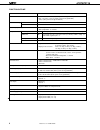
µ pd75p3116 2 data sheet u11369ej3v0ds function outline item function instruction execution time • 0.95, 1.91, 3.81, or 15.3 µ s (main system clock: @ 4.19 mhz) • 0.67, 1.33, 2.67, or 10.7 µ s (main system clock: @ 6.0 mhz) • 122 µ s (subsystem clock: @ 32.768 khz) internal memory prom 16384 × 8 bit...
Page 3
µ pd75p3116 3 data sheet u11369ej3v0ds contents 1. Pin configuration (top view) ................................................................................................. 4 2. Block diagram ..........................................................................................................
Page 4
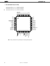
µ pd75p3116 4 data sheet u11369ej3v0ds 1. Pin configuration (top view) • 64-pin plastic qfp (14 × 14): µ pd75p3116gc-ab8 • 64-pin plastic lqfp (12 × 12): µ pd75p3116gk-8a8 • 64-pin plastic lqfp (14 × 14): µ pd75p3116gc-8bs note always connect the v pp pin directly to v dd during normal operation. 48...
Page 5
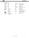
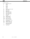
µ pd75p3116 5 data sheet u11369ej3v0ds pin identifications p00 to p03: port 0 com0 to com3: common output 0 to 3 p10 to p13: port 1 v lc0 to v lc2 : lcd power supply 0 to 2 p20 to p23: port 2 bias: lcd power supply bias control p30 to p33: port 3 lcdcl: lcd clock p50 to p53: port 5 sync: lcd synchro...
Page 6
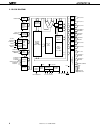
µ pd75p3116 6 data sheet u11369ej3v0ds 2. Block diagram p20 to p23 p00 to p03 s0 to s15 16 4 4 4 4 4 4 4 4 com0 to com3 4 bias f lcd v pp v dd reset vss cpu clock Φ standby control x2 x1 xt2 xt1 system clock generator main sub clock divider clock output control fx/2 n pcl/pto2/p22 general- purpose r...
Page 7
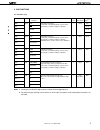
µ pd75p3116 7 data sheet u11369ej3v0ds 3. Pin functions 3.1 port pins (1/2) pin name i/o alternate function 8-bit status i/o circuit function i/o after reset type note 1 p00 input int4 4-bit input port (port 0) — input connection of an internal pull-up resistor can be p01 sck specified by a software...
Page 8
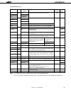
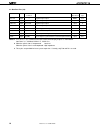
µ pd75p3116 8 data sheet u11369ej3v0ds 3.1 port pins (2/2) pin name i/o alternate function 8-bit status i/o circuit function i/o after reset type note 1 p60 i/o kr0/d0 programmable 4-bit i/o port (port 6) — input -a input and output can be specified in 1-bit units. P61 kr1/d1 connection of an intern...
Page 9
µ pd75p3116 9 data sheet u11369ej3v0ds 3.2 non-port pins (1/2) pin name i/o alternate function status i/o circuit function after reset type note 1 ti0 input p13 external event pulse input to timer/event counter input -c ti1 p12/int2/ti2 ti2 p12/int2/ti1 pto0 output p20 timer/event counter output inp...
Page 10
µ pd75p3116 10 data sheet u11369ej3v0ds 3.2 non-port pins (2/2) pin name i/o alternate function status i/o circuit function after reset type s0 to s15 output — segment signal output note 1 g-a s16 to s19 output p93 to p90 segment signal output input h s20 to s23 output p83 to p80 segment signal outp...
Page 11
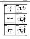
µ pd75p3116 11 data sheet u11369ej3v0ds 3.3 pin i/o circuits the i/o circuits for the µ pd75p3116’s pins are shown in abbreviated form below. In v dd p-ch n-ch v dd p-ch n-ch out data output disable in v dd p-ch in/out p.U.R. Enable data p.U.R. Type d output disable p.U.R. : pull-up resistor type a ...
Page 12
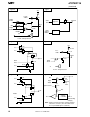
µ pd75p3116 12 data sheet u11369ej3v0ds (continued) type f-b type h type m-c type g-a type g-b type m-e output disable v dd p-ch n-ch in/out data v dd p-ch p.U.R. Enable p.U.R. Output disable (n) output disable (p) p.U.R. : pull-up resistor in/out type g-a type e-b seg data output disable data v dd ...
Page 13
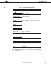
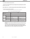
µ pd75p3116 13 data sheet u11369ej3v0ds 3.4 recommended connection of unused pins table 3-1. List of unused pin connections pin recommended connection p00/int4 connect to vss or v dd . P01/sck input: independently connect to vss or v dd via a resistor. P02/so/sb0 output: leave open. P03/si/sb1 conne...
Page 14
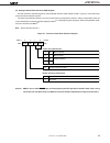
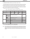
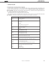
µ pd75p3116 14 data sheet u11369ej3v0ds 4. Mk i and mk ii mode selection function setting the stack bank selection (sbs) register for the µ pd75p3116 enables the program memory to be switched between the mk i mode and mk ii mode. This function is applicable when using the µ pd75p3116 to evaluate the...
Page 15
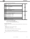
µ pd75p3116 15 data sheet u11369ej3v0ds 4.2 setting of stack bank selection (sbs) register use the stack bank selection register to switch between the mk i mode and mk ii mode. Figure 4-1 shows the format of the stack bank selection register. The stack bank selection register is set using a 4-bit me...
Page 16
µ pd75p3116 16 data sheet u11369ej3v0ds 5. Differences between µpd75p3116 and µpd753104, 753106, 753108 the µ pd75p3116 replaces the internal mask rom in the µ pd753104, 753106, and 753108 with a one-time prom and features expanded rom capacity. The µ pd75p3116’s mk i mode supports the mk i mode in ...
Page 17
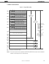
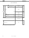
µ pd75p3116 17 data sheet u11369ej3v0ds 6. Memory configuration figure 6-1. Program memory map note can only be used in the mk ii mode. Remark for instructions other than those noted above, the br pcde and br pcxa instructions can be used to branch to addresses with changes in the pc’s lower 8 bits ...
Page 18
µ pd75p3116 18 data sheet u11369ej3v0ds figure 6-2. Data memory map note memory bank 0 or 1 can be selected as the stack area. (32 × 4) 256 × 4 (224 × 4) 128 × 4 0 1 15 000h 01fh 020h 0ffh 100h 1e0h 1dfh 1f7h 1f8h f80h fffh general-purpose register area display data memory data area static ram (512 ...
Page 19
µ pd75p3116 19 data sheet u11369ej3v0ds 7. Instruction set (1) representation and coding formats for operands in the instruction’s operand area, use the following coding format to describe operands corresponding to the instruction’s operand representations (for further details, refer to the ra75x as...
Page 20
µ pd75p3116 20 data sheet u11369ej3v0ds (2) operation conventions a: a register; 4-bit accumulator b: b register c: c register d: d register e: e register h: h register l: l register x: x register xa: register pair (xa); 8-bit accumulator bc: register pair (bc) de: register pair (de) hl: register pa...
Page 21
µ pd75p3116 21 data sheet u11369ej3v0ds (3) description of symbols used in addressing area remarks 1. Mb indicates access-enabled memory banks. 2. In area *2, mb = 0 for both mbe and mbs. 3. In areas *4 and *5, mb = 15 for both mbe and mbs. 4. Areas *6 to *11 indicate corresponding address-enabled a...
Page 22
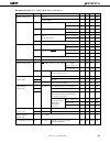
µ pd75p3116 22 data sheet u11369ej3v0ds instruction mnemonic operand no. Of machine operation addressing skip group bytes cycle area condition transfer mov a, #n4 1 1 a ← n4 string-effect a reg1, #n4 2 2 reg1 ← n4 xa, #n8 2 2 xa ← n8 string-effect a hl, #n8 2 2 hl ← n8 string-effect b rp2, #n8 2 2 r...
Page 23
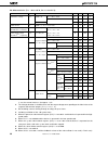
µ pd75p3116 23 data sheet u11369ej3v0ds instruction mnemonic operand no. Of machine operation addressing skip group bytes cycle area condition bit transfer mov1 cy, fmem.Bit 2 2 cy ← (fmem.Bit) *4 cy, pmem.@l 2 2 cy ← (pmem 7-2 +l 3-2 .Bit(l 1-0 )) *5 cy, @h+mem.Bit 2 2 cy ← (h+mem 3-0 .Bit) *1 fmem...
Page 24
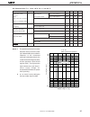
µ pd75p3116 24 data sheet u11369ej3v0ds instruction mnemonic operand no. Of machine operation addressing skip group bytes cycle area condition comparison ske reg, #n4 2 2+s skip if reg=n4 reg = n4 @hl, #n4 2 2+s skip if (hl)=n4 *1 (hl) = n4 a, @hl 1 1+s skip if a=(hl) *1 a = (hl) xa, @hl 2 2+s skip ...
Page 25
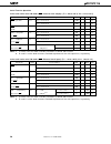
µ pd75p3116 25 data sheet u11369ej3v0ds instruction mnemonic operand no. Of machine operation addressing skip group bytes cycle area condition branch br note 1 addr — — pc 13-0 ← addr *6 use the assembler to select the most appropriate instruction among the following. • br !Addr • brcb !Caddr • br $...
Page 26
µ pd75p3116 26 data sheet u11369ej3v0ds instruction mnemonic operand no. Of machine operation addressing skip group bytes cycle area condition subroutine calla note !Addr1 3 3 (sp–6)(sp–3)(sp–4) ← pc 11-0 *11 stack control (sp–5) ← 0, 0, pc 13 , 12 (sp–2) ← x, x, mbe, rbe pc 13-0 ← addr1, sp ← sp–6 ...
Page 27
µ pd75p3116 27 data sheet u11369ej3v0ds instruction mnemonic operand no. Of machine operation addressing skip group bytes cycle area condition subroutine push rp 1 1 (sp–1)(sp–2) ← rp, sp ← sp–2 stack control bs 2 2 (sp–1) ← mbs, (sp–2) ← rbs, sp ← sp–2 pop rp 1 1 rp ← (sp+1)(sp), sp ← sp+2 bs 2 2 m...
Page 28
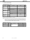
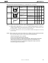
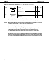
µ pd75p3116 28 data sheet u11369ej3v0ds 8. One-time prom (program memory) write and verify the program memory contained in the µ pd75p3116 is a 16384 × 8-bit one-time prom that can be electrically written one time only. The pins listed in the table below are used for this prom’s write/verify operati...
Page 29
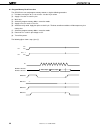
µ pd75p3116 29 data sheet u11369ej3v0ds 8.2 program memory write procedure program memory can be written at high speed using the following procedure. (1) pull down unused pins to vss via resistors. Set the x1 pin to low. (2) supply 5 v to the v dd and v pp pins. (3) wait 10 µ s. (4) select the progr...
Page 30
µ pd75p3116 30 data sheet u11369ej3v0ds v pp v dd v dd + 1 v dd v pp v dd x1 data output data output md0/p30 md2/p32 md3/p33 md1/p31 “l” d0/p60 to d3/p63 d4/p50 to d7/p53 8.3 program memory read procedure the µ pd75p3116 can read program memory contents using the following procedure. (1) pull down u...
Page 31
µ pd75p3116 31 data sheet u11369ej3v0ds 8.4 one-time prom screening due to its structure, the one-time prom cannot be fully tested before shipment by nec. Therefore, nec recommends that after the required data is written and the prom is stored under the temperature and time conditions shown below, t...
Page 32
µµµµµ pd75p3116 32 data sheet u11369ej3v0ds 9. Electrical specifications absolute maximum ratings (t a = 25˚c) parameter symbol test conditions rating unit power supply voltage v dd –0.3 to +7.0 v prom power supply v pp –0.3 to +13.5 v voltage input voltage v i1 except port 5 –0.3 to v dd + 0.3 v v ...
Page 33
µµµµµ pd75p3116 33 data sheet u11369ej3v0ds main system clock oscillator characteristics (t a = –40 to +85 ° c, v dd = 1.8 to 5.5 v) resonator recommended constant parameter test conditions min. Typ. Max. Unit ceramic oscillation 1.0 6.0 note 2 mhz resonator frequency (fx) note 1 oscillation after v...
Page 34
µ pd75p3116 34 data sheet u11369ej3v0ds subsystem clock oscillator characteristics (t a = –40 to +85˚c, v dd = 1.8 to 5.5 v) resonator recommended constant parameter test conditions min. Typ. Max. Unit crystal oscillation 32 32.768 35 khz resonator frequency (f xt ) note 1 oscillation v dd = 4.5 to ...
Page 35
µµµµµ pd75p3116 35 data sheet u11369ej3v0ds dc characteristics (t a = –40 to +85˚c, v dd = 1.8 to 5.5 v) parameter symbol test conditions min. Typ. Max. Unit output current, low i ol per pin 15 ma total of all pins 150 ma input voltage, high v ih1 ports 2, 3, 8, and 9 2.7 ≤ v dd ≤ 5.5 v 0.7v dd v dd...
Page 36
µµµµµ pd75p3116 36 data sheet u11369ej3v0ds dc characteristics (t a = –40 to +85˚c, v dd = 1.8 to 5.5 v) parameter symbol test conditions min. Typ. Max. Unit lcd drive voltage v lcd vac0 = 0 t a = –40 to +85 ° c 2.7 v dd v t a = –10 to +85 ° c 2.2 v dd v vac0 = 1 1.8 v dd v vac current note 1 i vac ...
Page 37
µ pd75p3116 37 data sheet u11369ej3v0ds ac characteristics (t a = –40 to +85˚c, v dd = 1.8 to 5.5 v) parameter symbol test conditions min. Typ. Max. Unit cpu clock cycle t cy operating on v dd = 2.7 to 5.5 v 0.67 64 µs time note 1 main system clock v dd = 1.8 to 5.5 v 0.95 64 µs (min. Instruction ex...
Page 38
µµµµµ pd75p3116 38 data sheet u11369ej3v0ds serial transfer operation 2-wire and 3-wire serial i/o mode (sck...Internal clock output): (t a = –40 to +85˚c, v dd = 1.8 to 5.5 v) parameter symbol test conditions min. Typ. Max. Unit sck cycle time t kcy1 v dd = 2.7 to 5.5 v 1300 ns v dd = 1.8 to 5.5 v ...
Page 39
µµµµµ pd75p3116 39 data sheet u11369ej3v0ds sbi mode (sck...Internal clock output (master)): (t a = –40 to +85˚c, v dd = 1.8 to 5.5 v) parameter symbol test conditions min. Typ. Max. Unit sck cycle time t kcy3 v dd = 2.7 to 5.5 v 1300 ns v dd = 1.8 to 5.5 v 3800 ns sck high-/low-level t kl3 , t kh3 ...
Page 40
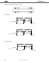
µ pd75p3116 40 data sheet u11369ej3v0ds ac timing test points (excluding x1, xt1 input) clock timing ti0, ti1, ti2 timing ti0, ti1, ti2 1/f ti t til t tih x1 input 1/f x t xl t xh 0.1 v v dd – 0.1 v xt1 input 1/f xt t xtl t xth 0.1 v v dd – 0.1 v v ih (min.) v il (max.) v ih (min.) v il (max.) v oh ...
Page 41
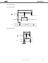
µ pd75p3116 41 data sheet u11369ej3v0ds serial transfer timing 3-wire serial i/o mode 2-wire serial i/o mode t kcy1, 2 t kl1, 2 t kh1, 2 sck si so t sik1, 2 t ksi1, 2 t kso1, 2 input data output data t kso1, 2 t sik1, 2 t kl1, 2 t kh1, 2 sck t ksi1, 2 sb0, 1 t kcy1, 2.
Page 42
µ pd75p3116 42 data sheet u11369ej3v0ds t kcy3, 4 t kh3, 4 t ksi3, 4 t sik3, 4 t kso3, 4 sck sb0, 1 t kl3, 4 t sbk t ksb t kcy3, 4 t kh3, 4 t ksi3, 4 t sik3, 4 t kso3, 4 sck sb0, 1 t kl3, 4 t sbk t sbh t sbl t ksb serial transfer timing bus release signal transfer command signal transfer interrupt i...
Page 43
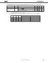
µ pd75p3116 43 data sheet u11369ej3v0ds data memory stop mode low supply voltage data retention characteristics (t a = –40 to +85˚c) parameter symbol test conditions min. Typ. Max. Unit release signal set time t srel 0 µ s oscillation stabilization t wait release by reset 2 15 /f x ms wait time note...
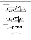
Page 44
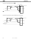
µ pd75p3116 44 data sheet u11369ej3v0ds data retention timing (stop mode release by reset) data retention timing (standby release signal: stop mode release by interrupt signal) v dd reset stop instruction execution stop mode data retention mode internal reset operation halt mode operating mode t sre...
Page 45
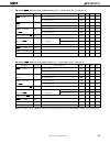
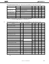
µµµµµ pd75p3116 45 data sheet u11369ej3v0ds dc programming characteristics (t a = 25 ± 5˚c, v dd = 6.0 ± 0.25 v, v pp = 12.5 ± 0.3 v, v ss = 0 v) parameter symbol test conditions min. Typ. Max. Unit input voltage, high v ih1 except x1 and x2 pins 0.7v dd v dd v v ih2 x1, x2 v dd – 0.5 v dd v input v...
Page 46
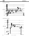
µ pd75p3116 46 data sheet u11369ej3v0ds program memory write timing program memory read timing t vps t vds t xh t xl t i t ds t dh t dv t df t ds t dh t ah t as t pw t m1r t m0s t opw t m1s t m1h t pcr t m3s t m3h data input data output data input data input v pp v dd v dd + 1 v dd v pp v dd x1 d0/p...
Page 47
µµµµµ pd75p3116 47 data sheet u11369ej3v0ds 10. Characteristic curves (reference values) 10 5.0 1.0 0.5 0.1 0.05 0.01 0.005 0.001 0 1 2 3 4 5 6 7 8 (t a = 25 ° c) supply voltage v dd (v) supply current i dd (ma) pcc = 0010 pcc = 0001 pcc = 0000 main system clock halt mode + 32 khz oscillation xt1 xt...
Page 48
µµµµµ pd75p3116 48 data sheet u11369ej3v0ds 10 5.0 1.0 0.5 0.1 0.05 0.01 0.005 0.001 0 1 2 3 4 5 6 7 8 xt1 xt2 x1 x2 crystal resonator 4.19 mhz crystal resonator 32.768 khz 330 k Ω 22 pf 22 pf 22 pf 22 pf supply voltage v dd (v) supply current i dd (ma) v dd v dd pcc = 0010 main system clock halt mo...
Page 49
µ pd75p3116 49 data sheet u11369ej3v0ds 48 49 32 64 1 17 16 33 64-pin plastic qfp (14x14) note each lead centerline is located within 0.15 mm of its true position (t.P.) at maximum material condition. Item millimeters a b d g 17.6 ± 0.4 14.0 ± 0.2 0.8 (t.P.) 1.0 j 17.6 ± 0.4 k p64gc-80-ab8-5 c 14.0 ...
Page 50
µ pd75p3116 50 data sheet u11369ej3v0ds 64-pin plastic lqfp (12x12) note each lead centerline is located within 0.13 mm of its true position (t.P.) at maximum material condition. Item millimeters a b d g 14.8 ± 0.4 12.0 ± 0.2 0.13 1.125 i 14.8 ± 0.4 j c 12.0 ± 0.2 h 0.32 ± 0.08 0.65 (t.P.) k 1.4 ± 0...
Page 51
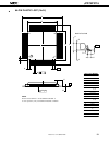
µ pd75p3116 51 data sheet u11369ej3v0ds 64-pin plastic lqfp (14x14) note each lead centerline is located within 0.20 mm of its true position (t.P.) at maximum material condition. Item millimeters a b d g 17.2 ± 0.2 14.0 ± 0.2 0.8 (t.P.) 1.0 j 17.2 ± 0.2 k c 14.0 ± 0.2 i 0.20 1.6 ± 0.2 l 0.8 f 1.0 n ...
Page 52
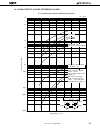
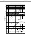
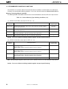
µ pd75p3116 52 data sheet u11369ej3v0ds 12. Recommended soldering conditions the µ pd75p3116 should be soldered and mounted under the conditions recommended in the table below. For details of recommended soldering conditions, refer to the information document semiconductor device mounting technology...
Page 53
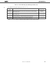
µ pd75p3116 53 data sheet u11369ej3v0ds table 12-1. Surface mounting type soldering conditions (2/2) (3) µ pd75p3116gc-8bs: 64-pin plastic lqfp (14 × 14) soldering soldering conditions recommended method condition symbol infrared reflow package peak temperature: 235 ° c, time: 30 seconds max. (at 21...
Page 54
µ pd75p3116 54 data sheet u11369ej3v0ds appendix a. List of µ pd75308b, 753108, and 75p3116 functions parameter µ pd75308b µ pd753108 µ pd75p3116 program memory mask rom mask rom one-time prom 0000h to 1f7fh 0000h to 1fffh 0000h to 3fffh (8064 × 8 bits) (8192 × 8 bits) (16384 × 8 bits) data memory 0...
Page 55
µ pd75p3116 55 data sheet u11369ej3v0ds parameter µ pd75308b µ pd753108 µ pd75p3116 clock output (pcl) Φ , 524, 262, 65.5 khz • Φ , 524, 262, 65.5 khz (main system clock: (main system clock: during 4.19 mhz operation) during 4.19 mhz operation) • Φ , 750, 375, 93.8 khz (main system clock: during 6.0...
Page 56
µ pd75p3116 56 data sheet u11369ej3v0ds appendix b. Development tools the following development tools have been provided for system development using the µ pd75p3116. In the 75xl series, a common relocatable assembler is used in combination with a device file dedicated to each model. Ra75x relocatab...
Page 57
µ pd75p3116 57 data sheet u11369ej3v0ds prom write tools hardware pg-1500 this is a prom writer that can program a single-chip microcontroller with prom in stand-alone mode or under the control of a host machine when connected with the supplied accessory board and optional programmer adapter. It can...
Page 58
µ pd75p3116 58 data sheet u11369ej3v0ds debugging tools an in-circuit emulator (ie-75001-r) is provided as a program debugging tool for the µ pd75p3116. The system configuration using this in-circuit emulator is shown below. Hardware ie-75001-r the ie-75001-r is an in-circuit emulator to be used for...
Page 59
µ pd75p3116 59 data sheet u11369ej3v0ds os for ibm pcs the following operating systems for ibm pcs are supported. Os version pc dos tm ver.3.1 to 6.3 j6.1/v note to j6.3/v note ms-dos ver.5.0 to 6.2 5.0/v note to 6.2/v note ibm dos tm j5.02/v note note only english mode is supported. Caution ver. 5....
Page 60
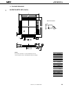
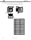
µ pd75p3116 60 data sheet u11369ej3v0ds package drawing and recommended footprint of conversion socket (ev-9200gc-64) figure b-1. Ev-9200gc-64 package drawing (for reference only) a f 1 e ev-9200gc-64 b d c m n l k r q i h p o s t j g no.1 pin index ev-9200gc-64-g0e item millimeters inches a b c d e...
Page 61
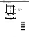
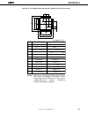
µ pd75p3116 61 data sheet u11369ej3v0ds figure b-2. Ev-9200gc-64 recommended footprint (for reference only) f e d g h i j k l c b a 0.031 × 0.591=0.472 0.031 × 0.591=0.472 ev-9200gc-64-p1e item millimeters inches a b c d e f g h i j k l 19.5 14.8 14.8 19.5 6.00 ± 0.08 6.00 ± 0.08 0.5 ± 0.02 2.36 ± 0...
Page 62
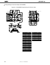
µ pd75p3116 62 data sheet u11369ej3v0ds package drawing of conversion adapter (tgk-064sbw) figure b-3. Tgk-064sbw package drawing (for reference only) item millimeters inches b 1.85 0.073 c 3.5 0.138 a 0.3 0.012 d 2.0 0.079 h 5.9 0.232 i 0.8 0.031 j 2.4 0.094 e 3.9 0.154 f 1.325 g 1.325 0.052 0.052 ...
Page 63
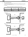
µ pd75p3116 63 data sheet u11369ej3v0ds notes on target system design the following shows a diagram of the connection conditions between the emulation probe, conversion connector and conversion socket or conversion adapter. Design your system making allowances for conditions such as the form of part...
Page 64
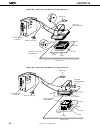
µ pd75p3116 64 data sheet u11369ej3v0ds figure b-6. Connection conditions of target system (1) figure b-7. Connection conditions of target system (2) in-circuit emulator ie-75001-r external sense clips target system conversion socket ev-9200gc-64 64-pin gc ep-753108gc-r ground clip 35 mm 35 mm 18.5 ...
Page 65
µ pd75p3116 65 data sheet u11369ej3v0ds appendix c. Related documents the related documents indicated in this publication may include preliminary versions. However, preliminary versions are not marked as such. Documents related to devices document name document no. µ pd753104, 753106, 753108 data sh...
Page 66
µ pd75p3116 66 data sheet u11369ej3v0ds other related documents document name document no. Semiconductor selection guide – products & packages – x13769e semiconductor device mounting technology manual c10535e quality grades on nec semiconductor devices c11531e nec semiconductor device reliability/qu...
Page 67
µ pd75p3116 67 data sheet u11369ej3v0ds [memo].
Page 68
µ pd75p3116 68 data sheet u11369ej3v0ds notes for cmos devices 1 precaution against esd for semiconductors note: strong electric field, when exposed to a mos device, can cause destruction of the gate oxide and ultimately degrade the device operation. Steps must be taken to stop generation of static ...
Page 69: Regional Information
µ pd75p3116 69 data sheet u11369ej3v0ds regional information some information contained in this document may vary from country to country. Before using any nec product in your application, piease contact the nec office in your country to obtain a list of authorized representatives and distributors. ...
Page 70
µ pd75p3116 qtop is a trademark of nec corporation. Ms-dos is either a registered trademark or a trademark of microsoft corporation in the united states and/or other countries. Ibm dos, pc/at, and pc dos are trademarks of international business machines corporation. The export of this product from j...

