- DL manuals
- NEC
- Computer Hardware
- PD78056F
- User Manual
NEC PD78056F User Manual
Summary of PD78056F
Page 1
User’s manual printed in japan © µ pd78058f, 78058fy subseries 8-bit single-chip microcontrollers µ pd78056f µ pd78058f µ pd78p058f µ pd78058f(a) µ pd78056fy µ pd78058fy µ pd78p058fy µ pd78058fy(a) document no. U12068ej2v0um00 (2nd edition) date published april 1998 n cp (k) 1997.
Page 2
2 [memo].
Page 3
3 notes for cmos devices 1 precaution against esd for semiconductors note: strong electric field, when exposed to a mos device, can cause destruction of the gate oxide and ultimately degrade the device operation. Steps must be taken to stop generation of static electricity as much as possible, and q...
Page 4
4 the export of this product from japan is regulated by the japanese government. To export this product may be prohibited without governmental license, the need for which must be judged by the customer. The export or re-export of this product from a country other than japan may also be prohibited wi...
Page 5: Regional Information
5 nec electronics inc. (u.S.) santa clara, california tel: 408-588-6000 800-366-9782 fax: 408-588-6130 800-729-9288 nec electronics (germany) gmbh duesseldorf, germany tel: 0211-65 03 02 fax: 0211-65 03 490 nec electronics (uk) ltd. Milton keynes, uk tel: 01908-691-133 fax: 01908-670-290 nec electro...
Page 6
6 major revisions in this edition page major revision from previous edition throughout the following products have already been developed: µ pd78056fgc- ××× -8bt, 78058fgc- ××× -8bt, 78p058fgc-8bt, 78056fygc- ××× -8bt, 78058fygc- ××× -8bt p133 to the block diagrams of the following ports were change...
Page 7
7 preface readers this manual has been prepared for user engineers who want to understand the functions of the µ pd78058f and 78058fy subseries and design and develop its application systems and programs. Affected versions are each of the versions in the following subseries. µ pd78058f subseries : µ...
Page 8
8 how to read this manual before reading this manual, you should have general knowledge of electric and logic circuits and microcontrollers. For persons who use this manual as the manual for the µ pd78058f(a) and 78058fy(a), → the µ pd78058f and 78058fy differ from the µ pd78058f(a) and 78058fy(a) o...
Page 9
9 chapter organization this manual divides the descriptions for the µ pd78058f and 78058fy subseries into different chapters as shown below. Read only the chapters related to the device you use. Chapter µ pd78058f subseries µ pd78058fy subseries chapter 1 outline ( µ pd78058f subseries) √ — chapter ...
Page 10
10 differences between µ pd78058f and µ pd78058fy subseries: the µ pd78058f and µ pd78058fy subseries are different in the following functions of the serial interface channel 0. Modes of serial interface channel 0 µ pd78058f µ pd78058fy subseries subseries 3-wire serial i/o mode √ √ 2-wire serial i/...
Page 11
11 related documents the related documents indicated in this publication may include preliminary versions. However, preliminary versions are not marked as such. Related documents for µ pd78058f subseries document name document no. Japanese english µ pd78056f, 78058f data sheet u11795j u11795e µ pd78...
Page 12
12 development tool documents (user’s manuals) document name document no. Japanese english ra78k0 assembler package operation u11802j u11802e assembly language u11801j u11801e structured assembler language u11789j u11789e ra78k series structured assembler preprocessor u12323j eeu-1402 cc78k0 c compi...
Page 13
13 documents for embedded software (user’s manual) document name document no. Japanese english 78k/0 series real-time os basics u11537j u11537e installation u11536j u11536e os for 78k/0 series mx78k0 basics u12257j u12257e other documents document name document no. Japanese english ic package manual...
Page 14
14 [memo].
Page 15
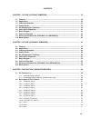
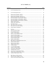
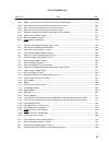
15 contents chapter 1 outline ( µ pd78058f subseries) ............................................................................. 35 1.1 features .................................................................................................................................. 35 1.2 applications ....
Page 16
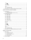
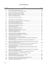
16 3.2.14 av ss .............................................................................................................................................. 71 3.2.15 reset ................................................................................................................................
Page 17
17 5.2.1 control registers ........................................................................................................................... 103 5.2.2 general registers ............................................................................................................................
Page 18
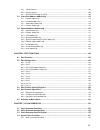
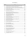
18 7.4.2 subsystem clock oscillator ........................................................................................................... 162 7.4.3 scaler ..............................................................................................................................................
Page 19
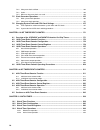
19 chapter 11 watchdog timer ...................................................................................................... 245 11.1 watchdog timer functions ................................................................................................ 245 11.2 watchdog timer configuration...
Page 20
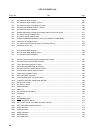
20 16.4.3 sbi mode operation ................................................................................................................. 305 16.4.4 2-wire serial i/o mode operation ............................................................................................. 331 16.4.5 sck0/p27...
Page 21
21 21.2 interrupt sources and configuration ................................................................................. 478 21.3 interrupt function control registers ................................................................................. 482 21.4 interrupt servicing operations .........
Page 22
22 26.3.3 prom read procedure ............................................................................................................ 546 26.4 screening of one-time prom versions ........................................................................... 547 chapter 27 instruction set ............
Page 23
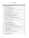
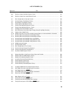
23 list of figures (1/8) figure no. Title page 3-1 list of pin input/output circuit .......................................................................................................... 75 4-1 list of pin input/output circuit ........................................................................
Page 24
24 list of figures (2/8) figure no. Title page 7-4 oscillation mode selection register format ..................................................................................... 159 7-5 main system clock waveform due to writing to osms .................................................................
Page 25
25 list of figures (3/8) figure no. Title page 8-31 control register settings for one-shot pulse output operation using software trigger ................ 204 8-32 timing of one-shot pulse output operation using software trigger ............................................... 205 8-33 control registe...
Page 26
26 list of figures (4/8) figure no. Title page 14-1 a/d converter block diagram ........................................................................................................... 263 14-2 a/d converter mode register format .......................................................................
Page 27
27 list of figures (5/8) figure no. Title page 16-27 address transmission from master device to slave device (wup = 1) .......................................... 325 16-28 command transmission from master device to slave device ......................................................... 326 16-29 data...
Page 28
28 list of figures (6/8) figure no. Title page 18-5 automatic data transmit/receive interval specify register format ................................................ 395 18-6 3-wire serial i/o mode timings .................................................................................................
Page 29
29 list of figures (7/8) figure no. Title page 20-4 real-time output port mode register format .................................................................................. 474 20-5 real-time output port control register format ......................................................................
Page 30
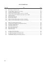
30 25-1 block diagram of rom correction ................................................................................................... 527 25-2 correction address registers 0 and 1 format .................................................................................. 528 25-3 correction cont...
Page 31
31 1-1 differences between the µ pd78058f and µ pd78058f(a) .............................................................. 45 1-2 mask options of mask pom versions .............................................................................................. 46 2-1 differences between the µ pd78058f...
Page 32
32 list of tables (2/3) table no. Title page 9-10 square-wave output ranges when 2-channel 8-bit timer/event counters (tm1 and tm2) are used as 16-bit timer/event counter ................................................................ 234 10-1 interval timer interval time .............................
Page 33
33 list of tables (3/3) table no. Title page 20-2 operation in real-time output buffer register manipulation ............................................................ 473 20-3 real-time output port operating mode and output trigger ............................................................. 475...
Page 34
34 [memo].
Page 35
35 chapter 1 outline ( µ pd78058f subseries) 1.1 features compared to the conventional µ pd78054 subseries, emi (electro magnetic interference) noise has been reduced. On-chip high-capacity rom and ram program memory (rom) part number item µ pd78056f µ pd78058f µ pd78p058f 48 kbytes 60 kbytes 60 kby...
Page 36
36 chapter 1 outline ( µ pd78058f subseries) 1.2 applications in the case of the µ pd78056f, 78058f and 78p058f, cellular phones, pagers, printers, av equipment, air conditioners, cameras, ppc’s, fuzzy home appliances, vending machines, etc. In the case of the µ pd78058f (a), controllers for car ele...
Page 37
37 chapter 1 outline ( µ pd78058f subseries) 1.4 quality grade part number package quality grade µ pd78056fgc- ××× -3b9 80-pin plastic qfp (14 × 14 mm, resin thickness: 2.7 mm) standard µ pd78056fgc- ××× -8bt 80-pin plastic qfp (14 × 14 mm, resin thickness: 1.4 mm) standard µ pd78058fgc- ××× -3b9 80...
Page 38
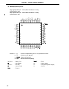
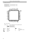
38 chapter 1 outline ( µ pd78058f subseries) 1.5 pin configuration (top view) (1) normal operating mode 80-pin plastic qfp (14 × 14 mm, resin thickness: 2.7 mm) µ pd78056fgc- ××× -3b9, 78058fgc- ××× -3b9, 78058fgc(a)- ××× -3b9, 78p058fgc-3b9 80-pin plastic qfp (14 × 14 mm, resin thickness: 1.4 mm) µ...
Page 39
39 chapter 1 outline ( µ pd78058f subseries) pin identifications a8 to a15 : address bus ad0 to ad7 : address/data bus ani0 to ani7 : analog input ano0, ano1 : analog output asck : asynchronous serial clock astb : address strobe av dd : analog power supply av ref0, 1 : analog reference voltage av ss...
Page 40
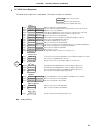
40 chapter 1 outline ( µ pd78058f subseries) (2) prom programming mode 80-pin plastic qfp (14 × 14 mm, resin thickness: 2.7 mm) µ pd78p058fgc-3b9 80-pin plastic qfp (14 × 14 mm, resin thickness: 1.4 mm) µ pd78p058fgc-8bt cautions 1. (l) : connect independently to v ss via a pull-down resistor. 2. V ...
Page 41
41 chapter 1 outline ( µ pd78058f subseries) 1.6 78k/0 series expansion the 78k/0 series expansion is shown below. The names in frames are subseries. Note under planning pd780964 pd78098 80-pin iebus controller was added to the pd78054 pd78044f 80-pin basic subseries for driving fip. Display output ...
Page 42
42 chapter 1 outline ( µ pd78058f subseries) the differences between the major functions of each subseries are shown below. Function rom timer 8-bit 10-bit 8-bit serial interface i/o v dd external subseries capacity 8-bit 16-bit watch wdt a/d a/d d/a min. Value extension control µ pd78075b 32 k to 4...
Page 43
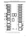
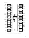
43 chapter 1 outline ( µ pd78058f subseries) 1.7 block diagram remarks 1. The internal rom and ram capacities depend on the product. 2. Pin connection in parentheses is intended for the µ pd78p058f. 16-bit timer/ event counter 8-bit timer/ event counter 1 watchdog timer watch timer serial interface ...
Page 44
44 chapter 1 outline ( µ pd78058f subseries) 1.8 outline of function rom mask rom prom 48 kbytes 60 kbytes 60 kbytes note 1 high-speed ram 1024 bytes 1024 bytes note 1 buffer ram 32 bytes expansion ram none 1024 bytes 1024 bytes note 2 memory space 64 kbytes general register 8 bits × 8 × 4 banks wit...
Page 45
45 chapter 1 outline ( µ pd78058f subseries) buzzer output 1.2 khz, 2.4 khz, 4.9 khz, 9.8 khz (main system clock at 5.0-mhz operation) vectored maskable internal: 13 interrupt external: 7 sources non-maskable internal: 1 software 1 test input internal: 1 external: 1 supply voltage v dd = 2.7 to 6.0 ...
Page 46
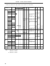
46 chapter 1 outline ( µ pd78058f subseries) 1.10 mask options there are mask options in the mask rom versions ( µ pd78056f, 78058f). By specifying the mask option when ordering, you can have the pull-up resistors shown in table 1-2 incorporated on-chip. If a mask option is used when pull-up resisto...
Page 47
47 chapter 2 outline ( µ pd78058fy subseries) 2.1 features compared to the conventional µ pd78054y subseries, emi (electro magnetic interference) noise has been reduced. On-chip high-capacity rom and ram notes 1. The capacities of internal prom and internal high-speed ram can be changed by means of ...
Page 48
48 chapter 2 outline ( µ pd78058fy subseries) 2.2 applications in the case of the µ pd78056fy, 78058fy and 78p058fy, cellular phones, pagers, printers, av equipment, air conditioners, cameras, ppcs, fuzzy home appliances, vending machines, etc. In the case of the µ pd78058fy (a), controllers for car...
Page 49
49 chapter 2 outline ( µ pd78058fy subseries) 2.4 quality grade part number package quality grade µ pd78056fygc- ××× -3b9 80-pin plastic qfp (14 × 14 mm, resin thickness: 2.7 mm) standard µ pd78056fygc- ××× -8bt 80-pin plastic qfp (14 × 14 mm, resin thickness: 1.4 mm) standard µ pd78058fygc- ××× -3b...
Page 50
50 chapter 2 outline ( µ pd78058fy subseries) 2.5 pin configuration (top view) (1) normal operating mode 80-pin plastic qfp (14 × 14 mm, resin thickness: 2.7 mm) µ pd78056fygc- ××× -3b9, 78058fygc- ××× -3b9, 78058fygc(a)- ××× -3b9, µ pd78p058fygc-3b9 80-pin plastic qfp (14 × 14 mm, resin thickness: ...
Page 51
51 chapter 2 outline ( µ pd78058fy subseries) pin identifications a8 to a15 : address bus ad0 to ad7 : address/data bus ani0 to ani7 : analog input ano0, ano1 : analog output asck : asynchronous serial clock astb : address strobe av dd : analog power supply av ref0, 1 : analog reference voltage av s...
Page 52
52 chapter 2 outline ( µ pd78058fy subseries) (2) prom programming mode 80-pin plastic qfp (14 × 14 mm, resin thickness: 2.7 mm) µ pd78p058fygc-3b9 80-pin plastic qfp (14 × 14 mm, resin thickness: 1.4 mm) µ pd78p058fygc-8bt note note under development cautions 1. (l) : connect independently to v ss ...
Page 53
53 chapter 2 outline ( µ pd78058fy subseries) 2.6 78k/0 series expansion the 78k/0 series expansion is shown below. The names in frames are subseries. Note under planning pd780964 pd78098 80-pin iebus controller was added to the pd78054 pd78044f 80-pin basic subseries for driving fip. Display output...
Page 54
54 chapter 2 outline ( µ pd78058fy subseries) the differences between the major functions of each subseries are shown below. Function rom serial interface i/o v dd subseries capacity min. Value control µ pd78078y 48 k to 60 k 3-wire/2-wire/i 2 c : 1 ch 88 1.8 v µ pd78070ay — 3-wire with automatic se...
Page 55
55 chapter 2 outline ( µ pd78058fy subseries) 2.7 block diagram remarks 1. The internal rom and ram capacities depend on the product. 2. Pin connection in parentheses is intended for the µ pd78p058fy. 16-bit timer/ event counter 8-bit timer/ event counter 1 watchdog timer watch timer serial interfac...
Page 56
56 chapter 2 outline ( µ pd78058fy subseries) 2.8 outline of function rom mask rom prom 48 kbytes 60 kbytes 60 kbytes note 1 high-speed ram 1024 bytes 1024 bytes note 1 buffer ram 32 bytes expansion ram none 1024 bytes 1024 bytes note 2 memory space 64 kbytes general register 8 bits × 8 × 4 banks wi...
Page 57
57 chapter 2 outline ( µ pd78058fy subseries) vectored maskable internal: 13 interrupt external: 7 sources non-maskable internal: 1 software 1 test input internal: 1 external: 1 supply voltage v dd = 2.7 to 6.0 v operating ambient temperature t a = –40 to +85 ° c package • 80-pin plastic qfp (14 × 1...
Page 58
58 chapter 2 outline ( µ pd78058fy subseries) 2.10 mask options the mask rom versions ( µ pd78056fy, 78058fy) provide pull-up resistor mask options which allow users to specify whether to connect a pull-up resistor to a specific port pin when the user places an order for the device production. Using...
Page 59
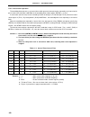
59 pin name input/output function after reset alternate function p00 input port 0. Input only input intp0/ti00 p01 input/ 8-bit input/output port. Input/output mode can be specified input intp1/ti01 p02 output bit-wise. Intp2 p03 if used as an input port, an on-chip intp3 p04 pull-up resistor can be...
Page 60
60 chapter 3 pin function ( µ pd78058f subseries) (1) port pins (2/3) pin name input/output function after reset alternate function p30 input/ port 3. Input to0 p31 output 8-bit input/output port. To1 p32 input/output mode can be specified bit-wise. To2 p33 if used as an input port, an on-chip pull-...
Page 61
61 chapter 3 pin function ( µ pd78058f subseries) (1) port pins (3/3) pin name input/output function after reset alternate function p120 to p127 input/ port 12. Input rtp0 to rtp7 output 8-bit input/output port. Input/output mode can be specified bit-wise. If used as an input port, an on-chip pull-u...
Page 62
62 chapter 3 pin function ( µ pd78058f subseries) (2) non-port pins (1/2) pin name input/output function after reset alternate function intp0 input external interrupt request inputs with specifiable valid edges (rising input p00/ti00 intp1 edge, falling edge, both rising and falling edges). P01/ti01...
Page 63
63 chapter 3 pin function ( µ pd78058f subseries) (2) non-port pins (2/2) pin name input/output function after reset alternate function ad0 to ad7 input/output low-order address/data bus when expanding external memory input p40 to p47 a8 to a15 output high-order address bus when expanding external m...
Page 64
64 chapter 3 pin function ( µ pd78058f subseries) 3.1.2 prom programming mode pins (prom versions only) pin name input/output function reset input prom programming mode setting. When +5 v or +12.5 v is applied to the v pp pin or a low level voltage is applied to the reset pin, the prom programming m...
Page 65
65 chapter 3 pin function ( µ pd78058f subseries) 3.2 description of pin functions 3.2.1 p00 to p07 (port 0) these are 8-bit input/output ports. Besides serving as input/output ports, they function as an external interrupt request input, an external count clock input to the timer, a capture trigger ...
Page 66
66 chapter 3 pin function ( µ pd78058f subseries) 3.2.2 p10 to p17 (port 1) these are 8-bit input/output ports. Besides serving as input/output ports, they function as an a/d converter analog input. The following operating modes can be specified bit-wise. (1) port mode these ports function as 8-bit ...
Page 67
67 chapter 3 pin function ( µ pd78058f subseries) (d) busy serial interface automatic transmit/receive busy input pins (e) stb serial interface automatic transmit/receive strobe output pins caution when this port is used as a serial interface pin, the i/o and output latches must be set according to ...
Page 68
68 chapter 3 pin function ( µ pd78058f subseries) 3.2.5 p40 to p47 (port 4) these are 8-bit input/output ports. Besides serving as input/output ports, they function as an address/data bus. The test input flag (krif) can be set to 1 by detecting a falling edge. The following operating mode can be spe...
Page 69
69 chapter 3 pin function ( µ pd78058f subseries) (1) port mode these ports function as 8-bit input/output ports. They can be specified bit-wise as input or output ports with port mode register 6 (pm6). P60 to p63 are n-ch open drain outputs. Mask rom version can contain pull-up resistors with the m...
Page 70
70 chapter 3 pin function ( µ pd78058f subseries) 3.2.9 p120 to p127 (port 12) these are 8-bit input/output ports. Besides serving as input/output ports, they function as a real-time output port. The following operating modes can be specified bit-wise. (1) port mode these ports function as 8-bit inp...
Page 71
71 chapter 3 pin function ( µ pd78058f subseries) 3.2.13 av dd this is the analog power supply pin of the a/d converter and the port’s power supply pin. Always use the same voltage as that of the v dd pin even when the a/d converter is not used. 3.2.14 av ss this is the ground potential pin for the ...
Page 72
72 chapter 3 pin function ( µ pd78058f subseries) 3.2.21 ic (mask rom version only) the ic (internally connected) pin is provided to set the test mode to check the µ pd78058f subseries at delivery. Connect it directly to the v ss with the shortest possible wire in the normal operating mode. When a v...
Page 73
73 chapter 3 pin function ( µ pd78058f subseries) pin name input/output input/output recommended connection of unused pins circuit type p00/intp0/ti00 2 input connect to v ss . P01/intp1/ti01 8-d input/output connect independently via a resistor to v ss. P02/intp2 p03/intp3 p04/intp4 p05/intp5 p06/i...
Page 74
74 chapter 3 pin function ( µ pd78058f subseries) table 3-1. Pin input/output circuit types (2/2) pin name input/output input/output recommended connection of unused pins circuit type p60 to p63 (mask rom version) 13-i input/output connect independently via a resistor to v dd . P60 to p63 (prom vers...
Page 75
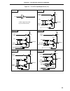
75 chapter 3 pin function ( µ pd78058f subseries) figure 3-1. List of pin input/output circuit (1/2) in pull-up enable av dd p-ch in/out input enable output disable data av dd p-ch n-ch type 2 type 5-j schmitt-triggered input with hysteresis characteristics type 5-o type 11-c type 10-c type 8-d pull...
Page 76
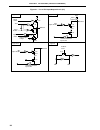
76 chapter 3 pin function ( µ pd78058f subseries) figure 3-1. List of pin input/output circuit (2/2) type 12-b type 13-h type 13-i output disable av dd n-ch in/out rd medium breakdown input buffer data p-ch xt2 xt1 feedback cut-off p-ch type 16 output disable av dd av dd n-ch mask option in/out rd m...
Page 77
77 chapter 4 pin function ( µ pd78058fy subseries) 4.1 pin function list 4.1.1 normal operating mode pins (1) port pins (1/3) pin name input/output function after reset alternate function p00 input port 0. Input only input intp0/ti00 p01 input/ 8-bit input/output port. Input/output mode can be speci...
Page 78
78 chapter 4 pin function ( µ pd78058fy subseries) n-ch open drain input/output port. On-chip pull-up resistor can be specified by mask option. (mask rom version only). Leds can be driven directly. (1) port pins (2/3) pin name input/output function after reset alternate function p30 input/ port 3. I...
Page 79
79 chapter 4 pin function ( µ pd78058fy subseries) (1) port pins (3/3) pin name input/output function after reset alternate function p120 to p127 input/ port 12. Input rtp0 to rtp7 output 8-bit input/output port. Input/output mode can be specified bit-wise. If used as an input port, an on-chip pull-...
Page 80
80 chapter 4 pin function ( µ pd78058fy subseries) (2) non-port pins (1/2) pin name input/output function after reset alternate function intp0 input external interrupt request inputs with specifiable valid edges (rising input p00/ti00 intp1 edge, falling edge, both rising and falling edges). P01/ti0...
Page 81
81 chapter 4 pin function ( µ pd78058fy subseries) (2) non-port pins (2/2) pin name input/output function after reset alternate function ad0 to ad7 input/output low-order address/data bus when expanding external memory input p40 to p47 a8 to a15 output high-order address bus when expanding external ...
Page 82
82 chapter 4 pin function ( µ pd78058fy subseries) 4.1.2 prom programming mode pins (prom versions only) pin name input/output function reset input prom programming mode setting. When +5 v or +12.5 v is applied to the v pp pin or a low level voltage is applied to the reset pin, the prom programming ...
Page 83
83 chapter 4 pin function ( µ pd78058fy subseries) 4.2 description of pin functions 4.2.1 p00 to p07 (port 0) these are 8-bit input/output ports. Besides serving as input/output ports, they function as an external interrupt request input, an external count clock input to the timer, a capture trigger...
Page 84
84 chapter 4 pin function ( µ pd78058fy subseries) 4.2.2 p10 to p17 (port 1) these are 8-bit input/output ports. Besides serving as input/output ports, they function as an a/d converter analog input. The following operating modes can be specified bit-wise. (1) port mode these ports function as 8-bit...
Page 85
85 chapter 4 pin function ( µ pd78058fy subseries) 4.2.4 p30 to p37 (port 3) these are 8-bit input/output ports. Beside serving as input/output ports, they function as timer input/output, clock output, and buzzer output. The following operating modes can be specified bit-wise. (1) port mode these po...
Page 86
86 chapter 4 pin function ( µ pd78058fy subseries) 4.2.5 p40 to p47 (port 4) these are 8-bit input/output ports. Besides serving as input/output ports, they function as an address/data bus. The test input flag (krif) can be set to 1 by detecting a falling edge. The following operating mode can be sp...
Page 87
87 chapter 4 pin function ( µ pd78058fy subseries) 4.2.8 p70 to p72 (port 7) this is a 3-bit input/output port. In addition to its use as an input/output port, it also has serial interface data input/ output and clock input/output functions. The following operating modes can be specified bit-wise. (...
Page 88
88 chapter 4 pin function ( µ pd78058fy subseries) 4.2.9 p120 to p127 (port 12) these are 8-bit input/output ports. Besides serving as input/output ports, they function as a real-time output port. The following operating modes can be specified bit-wise. (1) port mode these ports function as 8-bit in...
Page 89
89 chapter 4 pin function ( µ pd78058fy subseries) 4.2.13 av dd this is the analog power supply pin of the a/d converter and the port’s power supply pin. Always use the same voltage as that of the v dd pin even when the a/d converter is not used. 4.2.14 av ss this is the ground potential pin for the...
Page 90
90 chapter 4 pin function ( µ pd78058fy subseries) v ss ic as short as possible 4.2.21 ic (mask rom version only) the ic (internally connected) pin is provided to set the test mode to check the µ pd78058fy subseries at delivery. Connect it directly to the v ss with the shortest possible wire in the ...
Page 91
91 chapter 4 pin function ( µ pd78058fy subseries) pin name input/output input/output recommended connection of unused pins circuit type p00/intp0/ti00 2 input connect to v ss . P01/intp1/ti01 8-d input/output connect independently via a resistor to v ss. P02/intp2 p03/intp3 p04/intp4 p05/intp5 p06/...
Page 92
92 chapter 4 pin function ( µ pd78058fy subseries) table 4-1. Pin input/output circuit types (2/2) pin name input/output input/output recommended connection of unused pins circuit type p60 to p63 (mask rom version) 13-i input/output connect independently via a resistor to v dd . P60 to p63 (prom ver...
Page 93
93 chapter 4 pin function ( µ pd78058fy subseries) figure 4-1. List of pin input/output circuit (1/2) in pullup enable av dd p-ch in/out input enable output disable data av dd p-ch n-ch type 2 type 5-j schmitt-triggered input with hysteresis characteristics type 5-o type 11-c type 10-c type 8-d pull...
Page 94
94 chapter 4 pin function ( µ pd78058fy subseries) figure 4-1. List of pin input/output circuit (2/2) type 12-b type 13-h type 13-i output disable av dd n-ch in/out rd medium breakdown input buffer data p-ch xt2 xt1 feedback cut-off p-ch type 16 output disable av dd av dd n-ch mask option in/out rd ...
Page 95
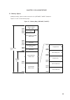
95 chapter 5 cpu architecture 5.1 memory spaces 64-kbyte memory spaces can be accessed in the µ pd78058f, 78058fy subseries. Figures 5-1 to 5-3 show memory maps. Figure 5-1. Memory map ( µ pd78056f, 78056fy) 0000h data memory space general registers 32 × 8 bits internal rom 49152 × 8 bits bfffh 1000...
Page 96
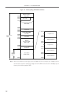
96 chapter 5 cpu architecture figure 5-2. Memory map ( µ pd78058f, 78058fy) note when internal rom size is 60 kbytes, the area f000h to f3ffh cannot be used. F000h to f3ffh can be used as external memory by setting the internal rom size to less than 56 kbytes by the memory size switching register (i...
Page 97
97 chapter 5 cpu architecture figure 5-3. Memory map ( µ pd78p058f, µ pd78p058fy) note when internal prom size is 60 kbytes, the area f000h to f3ffh cannot be used. F000h to f3ffh can be used as external memory by setting the internal prom size to less than 56 kbytes by the memory size switching reg...
Page 98
98 chapter 5 cpu architecture 5.1.1 internal program memory space the µ pd78056f and µ pd78056fy are mask rom with a 49152 x 8 bit configuration, the µ pd78058f and µ pd78058fy are mask rom with a 61440 x 8 bit configuration and the µ pd78p058f and µ pd78p058fy are prom with a 61440 x 8 bit configur...
Page 99
99 chapter 5 cpu architecture (2) callt instruction table area the 64-byte area 0040h to 007fh can store the subroutine entry address of a 1-byte call instruction (callt). (3) callf instruction entry area the area 0800h to 0fffh can perform a direct subroutine call with a 2-byte call instruction (ca...
Page 100
100 chapter 5 cpu architecture 5.1.5 data memory addressing the method to specify the address of the instruction to be executed next, or the address of a register or memory to be manipulated when an instruction is executed is called addressing. The address of the instruction to be executed next is a...
Page 101
101 chapter 5 cpu architecture figure 5-5. Data memory addressing ( µ pd78058f, 78058fy) note when internal rom size is 60 kbytes, the area f000h to f3ffh cannot be used. F000h to f3ffh can be used as external memory by setting the internal rom size to less than 56 kbytes by the memory size switchin...
Page 102
102 chapter 5 cpu architecture figure 5-6. Data memory addressing ( µ pd78p058f, 78p058fy) note when internal prom size is 60 kbytes, the area f000h to f3ffh cannot be used. F000h to f3ffh can be used as external memory by setting the internal prom size to less than 56 kbytes by the memory size swit...
Page 103
103 chapter 5 cpu architecture 5.2 processor registers the µ pd78058f and 78058fy subseries units incorporate the following processor registers. 5.2.1 control registers the control registers control the program sequence, statuses and stack memory. The control registers consist of a program counter (...
Page 104
104 chapter 5 cpu architecture (a) interrupt enable flag (ie) this flag controls the interrupt request acknowledge operations of the cpu. When ie = 0, all interrupts except non-maskable interrupt requests are disabled (di status). When ie = 1, interrupts are enabled (ei status). At this time, acknow...
Page 105
105 chapter 5 cpu architecture reti and retb instruction psw pc15-pc8 pc15-pc8 pc7-pc0 register pair lower sp sp + 2 sp register pair upper ret instruction pop rp instruction sp + 1 pc7-pc0 sp sp + 2 sp sp + 1 sp + 2 sp sp + 1 sp sp + 3 interrupt and brk instruction psw pc15-pc8 pc15-pc8 pc7-pc0 reg...
Page 106
106 chapter 5 cpu architecture 5.2.2 general registers a general register is mapped at particular addresses (fee0h to feffh) of the data memory. It consists of 4 banks, each bank consisting of eight 8-bit registers (x, a, c, b, e, d, l and h). Each register can also be used as an 8-bit register. Two...
Page 107
107 chapter 5 cpu architecture figure 5-12. General register configuration (a) absolute name (b) function name bank0 bank1 bank2 bank3 feffh fef8h fef7h fee0h rp3 rp2 rp1 rp0 r7 15 0 7 0 r6 r5 r4 r3 r2 r1 r0 16-bit processing 8-bit processing fee0h feefh fee8h fee7h bank0 bank1 bank2 bank3 feffh fef...
Page 108
108 chapter 5 cpu architecture 5.2.3 special function register (sfr) unlike a general register, each special-function register has special functions. It is allocated in the ff00h to ffffh area. The special-function register can be manipulated like the general register, with the operation, transfer a...
Page 109
109 chapter 5 cpu architecture address special-function register (sfr) name symbol r/w after reset ff00h port0 p0 r/w √ √ — 00h ff01h port1 p1 √ √ — ff02h port2 p2 √ √ — ff03h port3 p3 √ √ — ff04h port4 p4 √ √ — undefined ff05h port5 p5 √ √ — ff06h port6 p6 √ √ — ff07h port7 p7 √ √ — 00h ff0ch port1...
Page 110
110 chapter 5 cpu architecture address special-function register (sfr) name symbol r/w after reset ff38h correction address register 0 note corad0 r/w — — √ 0000h ff39h ff3ah correction address register 1 note corad1 — — √ ff3bh ff40h timer clock select register 0 tcl0 √ √ — 00h ff41h timer clock se...
Page 111
111 chapter 5 cpu architecture if0l if0h mk0l mk0h pr0l pr0h address special-function register (sfr) name symbol r/w after reset ffd0h to external access area note 1 r/w √ √ — undefined ffdfh ffe0h interrupt request flag register 0l √ √ ffe1h interrupt request flag register 0h √ √ ffe2h interrupt re...
Page 112
112 chapter 5 cpu architecture 15 0 pc + 15 0 8 7 6 s 15 0 pc α jdisp8 when s = 0, all bits of α are 0. When s = 1, all bits of α are 1. Pc indicates the start address of the instruction after the br instruction. ... 5.3 instruction address addressing an instruction address is determined by program ...
Page 113
113 chapter 5 cpu architecture 5.3.2 immediate addressing [function] immediate data in the instruction word is transferred to the program counter (pc) and branched. This function is carried out when the call !Addr16 or br !Addr16 or callf !Addr11 instruction is executed. The call !Addr16 and br !Add...
Page 114
114 chapter 5 cpu architecture 5.3.3 table indirect addressing [function] table contents (branch destination address) of the particular location to be addressed by bits 1 to 5 of the immediate data of an operation code are transferred to the program counter (pc) and branched. Before the callt [addr5...
Page 115
115 chapter 5 cpu architecture 7 0 rp 0 7 a x 15 0 pc 8 7 5.3.4 register addressing [function] register pair (ax) contents to be specified with an instruction word are transferred to the program counter (pc) and branched. This function is carried out when the br ax instruction is executed. [illustra...
Page 116
116 chapter 5 cpu architecture 5.4 operand address addressing the following various methods are available to specify the register and memory (addressing) which undergo manipulation during instruction execution. 5.4.1 implied addressing [function] the register which functions as an accumulator (a and...
Page 117
117 chapter 5 cpu architecture 5.4.2 register addressing [function] this addressing accesses a general register as an operand. The general register accessed is specified by the register bank select flags (rbs0 and rbs1) and register specify code (rn or rpn) in an instruction code. Register addressin...
Page 118
118 chapter 5 cpu architecture 5.4.3 direct addressing [function] this addressing directly addresses the memory indicated by the immediate data in an instruction word. [operand format] identifier description addr16 label or 16-bit immediate data [description example] mov a, !0fe00h; when setting !Ad...
Page 119
119 chapter 5 cpu architecture 5.4.4 short direct addressing [function] the memory to be manipulated in the fixed space is directly addressed with 8-bit data in an instruction word. The fixed space to which this address is applied is a 256-byte space of addresses fe20h through ff1fh. An internal ram...
Page 120
120 chapter 5 cpu architecture 15 0 short direct memory effective address 1 1 1 1 1 1 1 8 7 0 7 op code saddr-offset α [description example] mov 0fe30h, #50h; when setting saddr to fe30h and immediate data to 50h operation code 0 0 0 1 0 0 0 1 op code 0 0 1 1 0 0 0 0 30h (saddr-offset) 0 1 0 1 0 0 0...
Page 121
121 chapter 5 cpu architecture 15 0 sfr effective address 1 1 1 1 1 1 1 8 7 0 7 op code sfr-offset 1 5.4.5 special-function register (sfr) addressing [function] the memory-mapped special-function register (sfr) is addressed with 8-bit immediate data in an instruction word. This addressing is applied...
Page 122
122 chapter 5 cpu architecture 5.4.6 register indirect addressing [function] this addressing addresses the memory with the contents of a register pair specified as an operand. The register pair to be accessed is specified by the register bank select flags (rbs0 and rbs1) and register pair specify co...
Page 123
123 chapter 5 cpu architecture 5.4.7 based addressing [function] this addressing addresses the memory by adding 8-bit immediate data to the contents of the hl register pair which is used as a base register and by using the result of the addition. The hl register pair to be accessed is in the registe...
Page 124
124 chapter 5 cpu architecture 5.4.8 based indexed addressing [function] this addressing addresses the memory by adding the contents of the hl register, which is used as a base register, to the contents of the b or c register specified in the instruction word, and by using the result of the addition...
Page 125
125 chapter 6 port functions 6.1 port functions the µ pd78058f and 78058fy subseries units incorporate two input ports and sixty-seven input/output ports. Figure 6-1 shows the port configuration. Every port is capable of 1-bit and 8-bit manipulations and can carry out considerably varied control ope...
Page 126
126 chapter 6 port functions pin name function alternate function p00 port 0. Input only intp0/ti00 p01 8-bit input/output port. Input/output mode can be specified intp1/ti01 p02 bit-wise. Intp2 p03 if used as an input port, an on-chip pull-up intp3 p04 resistor can be used by software. Intp4 p05 in...
Page 127
127 chapter 6 port functions p70 si2/rxd p71 so2/txd p72 sck2/asck p120 to p127 rtp0 to rtp7 p130 and p131 ano0, ano1 table 6-1. Port functions ( µ pd78058f subseries) (2/2) pin name function alternate function p60 port 6. N-ch open-drain input/output port. — p61 8-bit input/output port. On-chip pul...
Page 128
128 chapter 6 port functions table 6-2. Port functions ( µ pd78058fy subseries) (1/2) pin name function alternate function p00 port 0. Input only intp0/ti00 p01 8-bit input/output port. Input/output mode can be specified intp1/ti01 p02 bit-wise. Intp2 p03 if used as an input port, an on-chip pull-up...
Page 129
129 chapter 6 port functions p120 to p127 rtp0 to rtp7 p130 and p131 ano0, ano1 p70 si2/rxd p71 so2/txd p72 sck2/asck table 6-2. Port functions ( µ pd78058fy subseries) (2/2) pin name function alternate function p60 port 6. N-ch open drain input/output port. — p61 8-bit input/output port. On-chip pu...
Page 130
130 chapter 6 port functions control register 6.2 port configuration a port consists of the following hardware: table 6-3. Port configuration item configuration port mode register (pmm: m = 0 to 3, 5 to 7, 12, 13) pull-up resistor option register (puoh, puol) memory expansion mode register (mm) note...
Page 131
131 chapter 6 port functions p00/intp0/ti00, p07/xt1 rd internal bus figure 6-2. P00 and p07 block diagram figure 6-3. P01 to p06 block diagram puo : pull-up resistor option register pm : port mode register rd : port 0 read signal wr : port 0 write signal p-ch wr pm wr port rd wr puo av dd p01/intp1...
Page 132
132 chapter 6 port functions 6.2.2 port 1 port 1 is an 8-bit input/output port with output latch. It can specify the input mode/output mode in 1-bit units with a port mode register 1 (pm1). When p10 to p17 pins are used as input ports, an on-chip pull-up resistor can be used to them in 8-bit units w...
Page 133
133 chapter 6 port functions 6.2.3 port 2 ( µ pd78058f subseries) port 2 is an 8-bit input/output port with output latch. P20 to p27 pins can specify the input mode/output mode in 1-bit units with the port mode register 2 (pm2). When p20 to p27 pins are used as input ports, an on-chip pull-up resist...
Page 134
134 chapter 6 port functions figure 6-6. P22 and p27 block diagram puo : pull-up resistor option register pm : port mode register rd : port 2 read signal wr : port 2 write signal p-ch wr pm wr port rd wr puo av dd selector puo2 output latch (p22, p27) pm22, pm27 internal bus alternate function p22/s...
Page 135
135 chapter 6 port functions 6.2.4 port 2 ( µ pd78058fy subseries) port 2 is an 8-bit input/output port with output latch. P20 to p27 pins can specify the input mode/output mode in 1-bit units with the port mode register 2 (pm2). When p20 to p27 pins are used as input ports, an on-chip pull-up resis...
Page 136
136 chapter 6 port functions figure 6-8. P22 and p27 block diagram puo : pull-up resistor option register pm : port mode register rd : port 2 read signal wr : port 2 write signal p-ch wr pm wr port rd wr puo av dd selector puo2 output latch (p22 and p27) pm22, pm27 internal bus alternate function p2...
Page 137
137 chapter 6 port functions 6.2.5 port 3 port 3 is an 8-bit input/output port with output latch. P30 to p37 pins can specify the input mode/output mode in 1-bit units with the port mode register 3 (pm3). When p30 to p37 pins are used as input ports, an on-chip pull-up resistor can be used to them i...
Page 138
138 chapter 6 port functions p40 p41 p42 p43 p44 p45 p46 p47 falling edge detection circuit krmk krif set signal standby release signal 6.2.6 port 4 port 4 is an 8-bit input/output port with output latch. P40 to p47 pins can specify the input mode/output mode in 8-bit units with the memory expansion...
Page 139
139 chapter 6 port functions 6.2.7 port 5 port 5 is an 8-bit input/output port with output latch. P50 to p57 pins can specify the input mode/output mode in 1-bit units with the port mode register 5 (pm5). When p50 to p57 pins are used as input ports, an on-chip pull-up resistor can be used to them i...
Page 140
140 chapter 6 port functions 6.2.8 port 6 port 6 is an 8-bit input/output port with output latch. P60 to p67 pins can specify the input mode/output mode in 1-bit units with the port mode register 6 (pm6). This port has functions related to pull-up resistors as shown below. These functions depending ...
Page 141
141 chapter 6 port functions figure 6-13. P60 to p63 block diagram pm : port mode register rd : port 6 read signal wr : port 6 write signal figure 6-14. P64 to p67 block diagram puo : pull-up resistor option register pm : port mode register rd : port 6 read signal wr : port 6 write signal wr pm wr p...
Page 142
142 chapter 6 port functions 6.2.9 port 7 this is a 3-bit input/output port with output latches. Input mode/output mode can be specified bit-wise by means of port mode register 7 (pm7). When pins p70 to p72 are used as input port pins, an on-chip pull-up resistor can be used as a 3-bit unit by means...
Page 143
143 chapter 6 port functions figure 6-16. P71 and p72 block diagram puo : pull-up resistor option register pm : port mode register rd : port 7 read signal wr : port 7 write signal p-ch wr pm wr port rd wr puo av dd selector puo7 output latch (p71 and p72) pm71, pm72 internal bus alternate function p...
Page 144
144 chapter 6 port functions 6.2.10 port 12 this is an 8-bit input/output port with output latches. Input mode/output mode can be specified bit-wise by means of port mode register 12 (pm12). When pins p120 to p127 are used as input port pins, an on-chip pull-up resistor can be used as an 8-bit unit ...
Page 145
145 chapter 6 port functions 6.2.11 port 13 this is a 2-bit input/output port with output latches. Input mode/output mode can be specified bit-wise by means of port mode register 13 (pm13). When pins p130 and p131 are used as input port pins, an on-chip pull-up resistor can be used as a 2-bit unit b...
Page 146
146 chapter 6 port functions 6.3 port function control registers the following four types of registers control the ports. • port mode registers (pm0 to pm3, pm5 to pm7, pm12, pm13) • pull-up resistor option register (puoh, puol) • memory expansion mode register (mm) • key return mode register (krm) ...
Page 147
147 chapter 6 port functions table 6-5. Port mode register and output latch settings when using alternate functions p00 intp0 input 1 (fixed) none ti00 input 1 (fixed) none p01 intp1 input 1 × ti01 input 1 × p02 to p06 intp2 to intp6 input 1 × p07 note 1 xt1 input 1 (fixed) none p10 to p17 note 1 an...
Page 148
148 chapter 6 port functions figure 6-19. Port mode register format pm0 pm1 pm2 1 pm06 pm03 pm02 pm01 1 7 6 5 4 3 2 1 0 symbol pm3 pm5 ff20h ff21h ff22h ff23h ff25h ffh ffh ffh ffh ffh r/w r/w r/w r/w r/w address after reset r/w pm17 pm16 pm15 pm14 pm13 pm12 pm11 pm10 pm27 pm26 pm25 pm24 pm23 pm22 p...
Page 149
149 chapter 6 port functions (2) pull-up resistor option register (puoh, puol) this register is used to set whether to use an internal pull-up resistor at each port or not. A pull-up resistor is internally used at bits which are set to the input mode at a port where on-chip pull-up resistor use has ...
Page 150
150 chapter 6 port functions (3) memory expansion mode register (mm) this register is used to set input/output of port 4. Mm is set with a 1-bit or 8-bit memory manipulation instruction. Reset input sets this register to 10h. Figure 6-21. Memory expansion mode register format note the full address m...
Page 151
151 chapter 6 port functions krif key return signal detection flag 0 1 not detected detected (falling edge detection of port 4) 0 0 0 0 krm fff6h 7 6 5 4 3 2 symbol 1 0 krmk krif 0 0 krmk standby mode control by key return signal 0 1 standby mode release enabled standby mode release disabled address...
Page 152
152 chapter 6 port functions 6.4 port function operations port operations differ depending on whether the input or output mode is set, as shown below. 6.4.1 writing to input/output port (1) output mode a value is written to the output latch by a transfer instruction, and the output latch contents ar...
Page 153
153 chapter 6 port functions 6.4.3 operations on input/output port (1) output mode an operation is performed on the output latch contents, and the result is written to the output latch. The output latch contents are output from the pins. Once data is written to the output latch, it is retained until...
Page 154
154 [memo].
Page 155
155 chapter 7 clock generator 7.1 clock generator functions the clock generator generates the clock to be supplied to the cpu and peripheral hardware. The following two types of system clock oscillators are available. (1) main system clock oscillator this circuit oscillates at frequencies of 1 to 5....
Page 156
156 chapter 7 clock generator figure 7-1. Block diagram of clock generator subsystem clock oscillator main system clock oscillator x2 x1 xt2 xt1/p07 frc stop mcc frc cls css pcc2 pcc1 internal bus standby control circuit to intp0 sampling clock 2 f xx 2 2 f xx 2 3 f xx 2 4 f xx prescaler clock to pe...
Page 157
157 chapter 7 clock generator 7.3 clock generator control register the clock generator is controlled by the following two registers: • processor clock control register (pcc) • oscillation mode selection register (osms) (1) processor clock control register (pcc) the pcc sets whether to use cpu clock ...
Page 158
158 chapter 7 clock generator figure 7-3. Processor clock control register format notes 1. Bit 5 is read only. 2. When the cpu is operating on the subsystem clock, mcc should be used to stop the main system clock oscillation. A stop instruction should not be used. Caution bit 3 must be set to 0. Rem...
Page 159
159 chapter 7 clock generator the fastest instruction of the µ pd78075f and 78075fy subseries can be executed in two clocks of the cpu clock. The relationship between the cpu clock (f cpu ) and the minimum instruction execution time is shown in table 7-2. Table 7-2. Relationship between cpu clock an...
Page 160
160 chapter 7 clock generator figure 7-5. Main system clock waveform due to writing to osms caution 2. When writing “1” to mcs, v dd must be 2.7 v or higher before the write execution. Remarks f xx : main system clock frequency (fx or fx/2) f x : main system clock oscillation frequency write to osms...
Page 161
161 chapter 7 clock generator 7.4 system clock oscillator 7.4.1 main system clock oscillator the main system clock oscillator oscillates with a crystal resonator or a ceramic resonator (standard: 5.0 mhz) connected to the x1 and x2 pins. External clocks can be input to the main system clock oscillat...
Page 162
162 chapter 7 clock generator 7.4.2 subsystem clock oscillator the subsystem clock oscillator oscillates with a crystal resonator (standard: 32.768 khz) connected to the xt1 and xt2 pins. External clocks can be input to the main system clock oscillator. In this case, input a clock signal to the xt1 ...
Page 163
163 chapter 7 clock generator figure 7-8. Examples of resonator with incorrect connection (2/2) (c) changing high current is too near a (d) current flows through the grounding line signal line of the resonator (potential at points a, b, and c fluctuate) (e) signals are fetched remark when using a su...
Page 164
164 chapter 7 clock generator 7.4.3 scaler the scaler divides the main system clock oscillator output (f xx ) and generates various clocks. 7.4.4 when no subsystem clocks are used if it is not necessary to use subsystem clocks for low power consumption operations and clock operations, connect the xt...
Page 165
165 chapter 7 clock generator 7.5 clock generator operations the clock generator generates the following various types of clocks and controls the cpu operating mode including the standby mode. • main system clock f xx • subsystem clock f xt • cpu clock f cpu • clock to peripheral hardware the follow...
Page 166
166 chapter 7 clock generator mcc css cls main system clock oscillation subsystem clock oscillation cpu clock l l oscillation does not stop. 7.5.1 main system clock operations when operated with the main system clock (with bit 5 (cls) of the processor clock control register (pcc) set to 0), the foll...
Page 167
167 chapter 7 clock generator mcc css cls main system clock oscillation subsystem clock oscillation cpu clock figure 7-9. Main system clock stop function (2/2) (c) operation when css is set after setting mcc with main system clock operation 7.5.2 subsystem clock operations when operated with the sub...
Page 168
168 chapter 7 clock generator table 7-3. Maximum time required for cpu clock switchover × × × × 1 0 0 0 1 1 0 0 1 0 0 0 1 0 0 0 css 0 0 0 0 × pcc0 pcc1 pcc2 1 × 1 pcc0 css pcc2 pcc1 0 0 0 0 1 1 0 0 0 1 0 0 0 0 1 × 1 × × 1 8 instructions 2 instructions 4 instructions 4 instructions 16 instructions 2 ...
Page 169
169 chapter 7 clock generator v dd reset interrupt request signal system clock cpu clock wait (26.2 ms : 5.0 mhz) internal reset operation minimum speed operation maximum speed operation subsystem clock operation f xx f xx f xt f xx high-speed operation 7.6.2 system clock and cpu clock switching pro...
Page 170
170 [memo].
Page 171
171 chapter 8 16-bit timer/event counter 8.1 overview of the µ pd78058f and 78058fy subseries on-chip timers this chapter describes the 16-bit timer/event counter and begins with an overview of the on-chip timers and related devices of the µ pd78058f and 78058fy subseries. (1) 16-bit timer/event cou...
Page 172
172 chapter 8 16-bit timer/event counter table 8-1. Timer/event counter operation interval timer 2 channels note 3 2 channels 1 channel note 1 1 channel note 2 external event counter √ √ — — timer output √ √ — — pwm output √ — — — pulse width measurement √ — — — square-wave output √ √ — — one-shot p...
Page 173
173 chapter 8 16-bit timer/event counter 8.2 16-bit timer/event counter functions the 16-bit timer/event counter (tm0) has the following functions. • interval timer • pwm output • pulse width measurement • external event counter • square-wave output • one-shot pulse output pwm output and pulse width...
Page 174
174 chapter 8 16-bit timer/event counter (5) square-wave output tm0 can output a square wave with any selected frequency. Table 8-3. 16-bit timer/event counter square-wave output ranges minimum pulse width maximum pulse width resolution mcs = 1 mcs = 0 mcs = 1 mcs = 0 mcs = 1 mcs = 0 2 × ti00 input ...
Page 175
175 chapter 8 16-bit timer/event counter tcl06 tcl05 tcl04 timer clock selection register 0 3 internal bus capture/compare control register 0 crc02 crc01 crc00 selector ti01/ p01/intp1 inttm3 2f xx f xx f xx /2 f xx /2 2 selector 16-bit capture/compare register 01 (cr01) internal bus 16-bit capture/...
Page 176
176 chapter 8 16-bit timer/event counter figure 8-2. 16-bit timer/event counter output control circuit block diagram remark the circuitry enclosed by the dotted line is the output control circuit. Pwm pulse output control circuit edge detection circuit ti00/p00/ intp0 ospt 16-bit timer output contro...
Page 177
177 chapter 8 16-bit timer/event counter (1) capture/compare register 00 (cr00) cr00 is a 16-bit register which has the functions of both a capture register and a compare register. Whether it is used as a capture register or as a compare register is set by bit 0 (crc00) of capture/compare control re...
Page 178
178 chapter 8 16-bit timer/event counter caution if the valid edge of the tio0/p00 pin is input while cr01 is read, cr01 does not perform the capture operation and retains the current data. However, the interrupt request flag (pif0) is set. (3) 16-bit timer register (tm0) tm0 is a 16-bit register wh...
Page 179
179 chapter 8 16-bit timer/event counter cloe tcl06 tcl05 tcl04 tcl03 tcl02 tcl01 tcl00 7 6 5 4 3 2 1 0 symbol tcl0 tcl03 tcl02 tcl01 tcl00 0 0 0 0 f xt (32.768 khz) 0 1 0 1 f xx f x (5.0 mhz) f x /2 (2.5 mhz) 0 1 1 0 f xx /2 f x /2 (2.5 mhz) f x /2 2 (1.25 mhz) 0 1 1 1 f xx /2 2 f x /2 2 (1.25 mhz)...
Page 180
180 chapter 8 16-bit timer/event counter remarks 1. F xx : main system clock frequency (f x or f x /2) 2. F x : main system clock oscillation frequency 3. F xt : subsystem clock oscillation frequency 4. Ti00 : 16-bit timer/event counter input pin 5. Tm0 : 16-bit timer register 6. Mcs : bit 0 of osci...
Page 181
181 chapter 8 16-bit timer/event counter 0 0 0 0 tmc03 tmc02 tmc01 ovf0 7 6 5 4 3 2 1 0 symbol tmc0 ff48h 00h r/w address after reset r/w ovf0 16-bit timer register overflow detection 0 overflow not detected 1 overflow detected tmc03 tmc02 tmc01 operating mode clear mode selection to0 output timing ...
Page 182
182 chapter 8 16-bit timer/event counter 0 0 0 0 0 crc02 crc01 crc00 7 6 5 4 3 2 1 0 symbol crc0 ff4ch 04h r/w address after reset r/w crc00 cr00 operating mode selection 0 operates as compare register 1 operates as capture register crc01 cr00 capture trigger selection captures on valid edge of ti01...
Page 183
183 chapter 8 16-bit timer/event counter 0 ospt ospe toc04 lvs0 lvr0 toc01 toe0 7 6 5 4 3 2 1 0 symbol toc0 ff4eh 00h r/w address after reset r/w toe0 16-bit timer/event counter output control 0 output disabled (port mode) 1 output enabled toc01 0 1 in pwm mode in other modes active level selection ...
Page 184
184 chapter 8 16-bit timer/event counter pm37 pm36 pm35 pm34 pm33 pm32 pm31 pm30 7 6 5 4 3 2 1 0 symbol pm3 ff23h ffh r/w address after reset r/w pm3n p3n pin input/output mode selection (n = 0 to 7) 0 output mode (output buffer on) 1 input mode (output buffer off) (5) port mode register 3 (pm3) thi...
Page 185
185 chapter 8 16-bit timer/event counter es31 es30 es21 es20 es11 es10 0 0 7 6 5 4 3 2 1 0 symbol intm0 ffech 00h r/w address after reset r/w es11 intp0 valid edge selection es10 0 falling edge 0 0 rising edge 1 1 setting prohibited 0 1 both falling and rising edges 1 es21 intp1 valid edge selection...
Page 186
186 chapter 8 16-bit timer/event counter 0 0 0 0 0 0 scs1 scs0 7 6 5 4 3 2 1 0 symbol scs ff47h 00h r/w address after reset r/w scs1 scs0 0 0 0 1 1 0 1 1 intp0 sampling clock selection mcs = 1 mcs = 0 f xx /2 n f x /2 7 (39.1 khz) f xx /2 7 f x /2 8 (19.5 khz) f x /2 5 (156.3 khz) f xx /2 5 f x /2 6...
Page 187
187 chapter 8 16-bit timer/event counter 0 0 0 0 0 0/1 0/1 0 crc02 crc01 crc00 crc0 cr00 set as compare register 0 0 0 0 1 1 0/1 0 tmc03 tmc02 tmc01 ovf0 tmc0 clear & start on match tm0 and cr00 8.5 16-bit timer/event counter operations 8.5.1 interval timer operations setting the 16-bit timer mode c...
Page 188
188 chapter 8 16-bit timer/event counter 16-bit capture/compare register 00 (cr00) 16-bit timer register (tm0) selector f xx /2 2 f xx /2 f xx 2f xx inttm3 ti00/p00/intp0 ovf0 clear circuit inttm00 figure 8-11. Interval timer configuration diagram figure 8-12. Interval timer operation timings remark...
Page 189
189 chapter 8 16-bit timer/event counter table 8-6. 16-bit timer/event counter interval times minimum interval time maximum interval time resolution mcs = 1 mcs = 0 mcs = 1 mcs = 0 mcs = 1 mcs = 0 0 0 0 2 × ti00 input cycle 2 16 × ti00 input cycle ti00 input edge cycle 0 0 1 setting 2 × 1/f x settin...
Page 190
190 chapter 8 16-bit timer/event counter toe0 toc01 lvr0 lvs0 toc04 ospe ospt toc0 1 0/1 × × × × × 0 to0 output enabled specifies active level crc00 crc01 crc02 crc0 0 0/1 0/1 0 0 0 0 0 cr00 set as compare register tmc0 0 1 0 0 0 0 0 0 ovf0 tmc01 tmc02 tmc03 pwm mode figure 8-13. Control register se...
Page 191
191 chapter 8 16-bit timer/event counter by integrating 14-bit resolution pwm pulses with an external low-pass filter, they can be converted to an analog voltage and used for electronic tuning and d/a converter applications, etc. The analog output voltage (v an ) used for d/a conversion with the con...
Page 192
192 chapter 8 16-bit timer/event counter toc0 1 1 0/1 0/1 1 0 0 0 toe0 toc01 lvr0 lvs0 inversion of output on match of tm0 and cr00 toc04 ospe ospt to0 output enabled specified to0 output f/f initial value inversion of output on match of tm0 and cr01 one-shot pulse output disabled crc0 0 x 0 0 0 0 0...
Page 193
193 chapter 8 16-bit timer/event counter tmc0 0 0/1 1 0 0 0 0 0 ovf0 tmc01 tmc02 tmc03 free-running mode crc0 0 0/1 1 0 0 0 0 0 crc00 crc01 crc02 cr00 set as compare register cr01 set as capture register 8.5.4 pulse width measurement operations it is possible to measure the pulse width of the signal...
Page 194
194 chapter 8 16-bit timer/event counter selector f xx /2 2 f xx /2 f xx 2f xx inttm3 16-bit timer register (tm0) 16-bit capture/compare register 01 (cr01) ovf0 intp0 internal bus ti00/p00/intp00 count clock tm0 count value ti00 pin input cr01 captured value intp0 ovf0 0000 0001 d0 d1 ffff 0000 d2 d...
Page 195
195 chapter 8 16-bit timer/event counter crc0 1 0 1 0 0 0 0 0 crc00 crc01 crc02 cr00 set as capture register captured in cr00 on valid edge of ti01/p01 pin cr01 set as capture register tmc0 0 0/1 1 0 0 0 0 0 ovf0 tmc01 tmc02 tmc03 free-running mode (2) measurement of two pulse widths with free-runni...
Page 196
196 chapter 8 16-bit timer/event counter count clock tm0 count value ti00 pin input cr01 captured value intp0 ti01 pin input t cr00 captured value intp1 ovf0 (d1 – d0) × t (10000h – d1 + d2) × t (10000h – d1 + (d2 + 1)) × t (d3 – d2) × t 0000 0001 d0 d1 0000 d3 d2 ffff d0 d1 d3 d2 d1 figure 8-21. Ti...
Page 197
197 chapter 8 16-bit timer/event counter crc0 1 1 1 0 0 0 0 0 crc00 crc01 crc02 cr00 set as capture register captured in cr00 on invalid edge of ti00/p00 pin cr01 set as capture register tmc0 0 0/1 1 0 0 0 0 0 ovf0 tmc01 tmc02 tmc03 free-running mode (3) pulse width measurement with free-running cou...
Page 198
198 chapter 8 16-bit timer/event counter count clock tm0 count value ti00 pin input cr01 captured value cr00 captured value intp0 ovf0 (d1-d0) × t (10000h-d1 + d2) × t (d3-d2) × t d1 d3 d0 d2 d3 d2 0000 ffff d1 d0 0000 0001 t figure 8-23. Timing of pulse width measurement operation by free-running c...
Page 199
199 chapter 8 16-bit timer/event counter crc0 1 1 1 0 0 0 0 0 crc00 crc01 crc02 cr00 set as capture register captured in cr00 on invalid edge of ti00/p00 pin cr01 set as capture register tmc0 0 0/1 0 1 0 0 0 0 ovf0 tmc01 tmc02 tmc03 clear & start with valid edge of ti00/p00 pin (4) pulse width measu...
Page 200
200 chapter 8 16-bit timer/event counter crc0 0 0/1 0/1 0 0 0 0 0 crc00 crc01 crc02 cr00 set as compare register tmc0 0 0/1 1 1 0 0 0 0 ovf0 tmc01 tmc02 tmc03 clear & start with match of tm0 and cr00 8.5.5 external event counter operation the external event counter counts the number of external cloc...
Page 201
201 chapter 8 16-bit timer/event counter ti00 pin input tm0 count value cr00 inttm0 n 0000 0001 0002 0003 0004 0005 n-1 n 0000 0001 0002 0003 16-bit capture/compare register 00 (cr00) clear inttm00 intp0 16-bit timer register (tm0) 16-bit capture/compare register 01 (cr01) internal bus ti00 valid ed...
Page 202
202 chapter 8 16-bit timer/event counter toc0 1 1 0/1 0/1 0 0 0 0 toe0 toc01 lvr0 ospt ospe toc04 lvs0 to0 output enabled inversion of output on match of tm0 and cr00 specified to0 output f/f initial value no inversion of output on match of tm0 and cr01 one-shot pulse output disabled crc0 0 0/1 0/1 ...
Page 203
203 chapter 8 16-bit timer/event counter count clock tm0 count value cr00 inttm00 to0 pin output 0000 0001 0002 n-1 n 0000 0001 0002 n-1 n 0000 n figure 8-30. Square-wave output operation timing table 8-7. 16-bit timer/event count square-wave output ranges minimum pulse width maximum pulse width res...
Page 204
204 chapter 8 16-bit timer/event counter toc0 1 1 0/1 0/1 1 1 0 0 toe0 toc01 lvr0 ospt ospe toc04 lvs0 to0 output enabled inversion of output on match of tm0 and cr00 specified to0 output f/f initial value inversion of output on match of tm0 and cr01 one-shot pulse output mode set 1 in case of outpu...
Page 205
205 chapter 8 16-bit timer/event counter count clock tm0 count value cr01 set value cr00 set value inttm01 ospt inttm00 to0 pin output 0000 0001 n n+1 0000 n-1 n m-1 m 0000 0001 0002 n m n m n m n m set 0ch to tmc0 (tm0 count start) figure 8-32. Timing of one-shot pulse output operation using softwa...
Page 206
206 chapter 8 16-bit timer/event counter crc0 0 0/1 0 0 0 0 0 0 crc00 crc01 crc02 cr00 set as compare register cr01 set as compare register toc0 1 1 0/1 0/1 1 1 0 0 toe0 toc01 lvr0 lvs0 ospt ospe toc04 to0 output enabled inversion of output on match of tm0 and cr00 specified to0 output f/f initial v...
Page 207
207 chapter 8 16-bit timer/event counter count clock tm0 count value cr01 set value cr00 set value inttm01 ti00 pin input inttm00 to0 pin output 0000 0001 0000 n n+1 n+2 m–2 m–1 m m+1 m+2 m+3 n m n m n m n m set 08h to tmc0 (tm0 count start) figure 8-34. Timing of one-shot pulse output operation usi...
Page 208
208 chapter 8 16-bit timer/event counter count pulse cr00 tm0 count value x-1 x ffffh 0000h 0001h 0002h m n timer start count pulse tm0 count value 0000h 0001h 0002h 0003h 0004h 8.6 16-bit timer/event counter operating precautions (1) timer start errors an error with a maximum of one clock may occur...
Page 209
209 chapter 8 16-bit timer/event counter count pulse tm0 count value edge input interrupt request flag capture read signal cr01 captured value capture operation ignored x n+1 n n+1 n+2 m m+1 m+2 (4) capture register data retention timings if the valid edge of the ti00/p00 pin is input during 16-bit ...
Page 210
210 chapter 8 16-bit timer/event counter count pulse cr00 tm0 ovf0 inttm00 ffffh fffeh ffffh 0000h 0001h (7) operation of ovf0 flag ofv0 flag is set to 1 in the following case. The clear & start mode on match between tm0 and cr00 is selected. ↓ cr00 is set to ffffh. ↓ when tm0 is counted up from fff...
Page 211
211 chapter 9 8-bit timer/event counters 9.1 8-bit timer/event counter function the on-chip 8-bit timer/event counters of the µ pd78058f, 78058fy subseries have two modes: a mode in which the two 8-bit timer/event counter channels are separately used (8-bit timer/event counter mode), and a mode in w...
Page 212
212 chapter 9 8-bit timer/event counters (1) 8-bit interval timer interrupt requests are generated at the preset time intervals. Table 9-1. 8-bit timer/event counter interval times minimum interval time maximum interval time resolution mcs = 1 mcs = 0 mcs = 1 mcs = 0 mcs = 1 mcs = 0 2 × 1/f x 2 2 × ...
Page 213
213 chapter 9 8-bit timer/event counters (2) external event counter the number of pulses of an externally input signal can be measured. (3) square-wave output a square wave with any selected frequency can be output. Table 9-2. 8-bit timer/event counter square-wave output ranges minimum pulse width m...
Page 214
214 chapter 9 8-bit timer/event counters 9.1.2 16-bit timer/event counter mode (1) 16-bit interval timer interrupt requests can be generated at the preset time intervals. Table 9-3. Interval times when 8-bit timer/event counters are used as 16-bit timer/event counter minimum interval time maximum in...
Page 215
215 chapter 9 8-bit timer/event counters (2) external event counter the number of pulses of an externally input signal can be measured. (3) square-wave output a square wave with any selected frequency can be output. Table 9-4. Square-wave output ranges when 8-bit timer/event counters are used as 16-...
Page 216
216 chapter 9 8-bit timer/event counters 9.2 8-bit timer/event counter configuration the 8-bit timer/event counters 1 and 2 consist of the following hardware. Table 9-5. 8-bit timer/event counter configuration item configuration timer register 8 bits × 2 (tm1, tm2) register compare register: 8 bits ...
Page 217
217 chapter 9 8-bit timer/event counters figure 9-1. 8-bit timer/event counter block diagram note refer to figures 9-2 and 9-3 for details of 8-bit timer/event counters 1 and 2 output control circuits 1 and 2, respectively. 8-bit compare register 10 (cr10) match 8-bit timer register 1 (tm1) selector...
Page 218
218 chapter 9 8-bit timer/event counters lvr2 lvs2 toc15 inttm2 r s inv level f/f (lv2) f sck p32 output latch pm32 toe2 to2/p32 q lvr1 lvs1 toc11 inttm1 r s inv q p31 output latch toe1 pm31 to1/p31 level f/f (lv1) figure 9-2. Block diagram of 8-bit timer/event counter output control circuit 1 remar...
Page 219
219 chapter 9 8-bit timer/event counters (1) compare registers 10 and 20 (cr10, cr20) these are 8-bit registers to compare the value set to cr10 to the 8-bit timer register 1 (tm1) count value, and the value set to cr20 to the 8-bit timer register 2 (tm2) count value, and, if they match, generate an...
Page 220
220 chapter 9 8-bit timer/event counters 9.3 8-bit timer/event counter control registers the following four types of registers are used to control the 8-bit timer/event counter. • timer clock select register 1 (tcl1) • 8-bit timer mode control register 1 (tmc1) • 8-bit timer output control register ...
Page 221
221 chapter 9 8-bit timer/event counters tcl17 tcl16 tcl15 tcl14 tcl13 tcl12 tcl11 tcl10 7 6 5 4 3 2 1 0 symbol tcl1 ff41h 00h r/w address after reset r/w tcl13 tcl12 tcl11 tcl10 0 0 0 0 ti1 falling edge 0 0 0 1 ti1 rising edge 0 1 1 0 0 1 1 1 f xx /2 f x /2 (2.5 mhz) f x /2 2 (1.25 mhz) 1 0 0 0 f x...
Page 222
222 chapter 9 8-bit timer/event counters 0 1 2 3 4 5 6 7 symbol tce1 ff49h 00h r/w address after reset r/w tce2 tmc12 0 0 0 0 0 tmc1 tce1 8-bit timer register 1 operation control 0 operation stop (tm1 clear to 0) 1 operation enable tce2 8-bit timer register 2 operation control operation stop (tm2 cl...
Page 223
223 chapter 9 8-bit timer/event counters 0 1 2 3 4 5 6 7 symbol toe1 toc11 lvr1 lvs1 toe2 toc15 lvr2 lvs2 toc1 ff4fh 00h r/w address after reset r/w toe1 8-bit timer/event counter 1 outptut control 0 output disable (port mode) 1 output enable toc11 8-bit timer/event counter 1 timer output f/f contro...
Page 224
224 chapter 9 8-bit timer/event counters 0 1 2 3 4 5 6 7 symbol pm30 ff23h ffh r/w address after reset r/w pm31 pm32 pm33 pm34 pm35 pm36 pm37 pm3 pm3n p3n pin input/output mode selection (n=0 to 7) 0 output mode (output buffer on) 1 input mode (output buffer off) (4) port mode register 3 (pm3) this ...
Page 225
225 chapter 9 8-bit timer/event counters 9.4 8-bit timer/event counter operation 9.4.1 8-bit timer/event counter mode (1) interval timer operations operates as an interval timer which generates interrupt requests repeatedly with the count values set previously in the 8 bit conveyor registers 10 and ...
Page 226
226 chapter 9 8-bit timer/event counters table 9-6. 8-bit timer/event counter 1 interval time minimum interval time maximum interval time resolution mcs = 1 mcs = 0 mcs = 1 mcs = 0 mcs = 1 mcs = 0 0 0 0 0 ti1 input cycle 2 8 × ti1 input cycle ti1 input edge cycle 0 0 0 1 ti1 input cycle 2 8 × ti1 in...
Page 227
227 chapter 9 8-bit timer/event counters table 9-7. 8-bit timer/event counter 2 interval time minimum interval time maximum interval time resolution mcs = 1 mcs = 0 mcs = 1 mcs = 0 mcs = 1 mcs = 0 0 0 0 0 ti2 input cycle 2 8 × ti2 input cycle ti2 input edge cycle 0 0 0 1 ti2 input cycle 2 8 × ti2 in...
Page 228
228 chapter 9 8-bit timer/event counters ti1 pin input tm1 count value inttm1 cr10 00 01 02 03 04 05 n-1 n 00 01 02 03 n (2) external event counter operation the external event counter counts the number of external clock pulses to be input to the ti1/p33 and ti2/ p34 pins with 8-bit timer registers ...
Page 229
229 chapter 9 8-bit timer/event counters (3) operation as a square wave output operates as a square wave output at the desired frequency with the values set previously in the 8 bit conveyor registers 10 and 20 (cr10, cr20) as the interval. The to1/p31 or to2/p32 pin output status is reversed at inte...
Page 230
230 chapter 9 8-bit timer/event counters figure 9-10. Square-wave output operation timing note the initial value of to1 output can be set with bits 2 and 3 (lvr1 and lvs1) of the 8-bit timer output control register (toc1). 9.4.2 16-bit timer/event counter mode when bit 2 (tmc12) of the 8-bit timer m...
Page 231
231 chapter 9 8-bit timer/event counters figure 9-11. Interval timer operation timing remark interval time = (n + 1) × t : n = 0000h to ffffh caution even if the 16-bit timer/event counter mode is used, when the tm1 count value matches the cr10 value, interrupt request (inttm1) is generated and the ...
Page 232
232 chapter 9 8-bit timer/event counters table 9-9. Interval times when 2-channel 8-bit timer/event counters (tm1 and tm2) are used as 16-bit timer/event counter minimum interval time maximum interval time resolution mcs = 1 mcs = 0 mcs = 1 mcs = 0 mcs = 1 mcs = 0 0 0 0 0 ti1 input cycle 2 8 × ti1 i...
Page 233
233 chapter 9 8-bit timer/event counters ti1 pin input tm1, tm2 count value cr10, cr20 inttm2 0000 0001 0002 0003 0004 0005 n-1 n 0000 0001 0002 0003 n (2) external event counter operations the external event counter counts the number of external clock pulses to be input to the ti1/p33 pin with 2- c...
Page 234
234 chapter 9 8-bit timer/event counters (3) operation as a square wave output operates as a square wave output at the desired frequency with the values set previously in the 8 bit conveyor registers 10 and 20 (cr10, cr20) as the interval. When setting the count value, the value of the upper 8 bits ...
Page 235
235 chapter 9 8-bit timer/event counters figure 9-13. Square-wave output operation timing count clock tm1 00h 00h 00h 01h ffh 00h 01h 02h ffh 00h 01h ffh m – 1 00h 00h m 01h n n n m n + 1 tm2 cr10 cr20 to2 count start level inversion counter clear interval time.
Page 236
236 chapter 9 8-bit timer/event counters ti1, ti2, input cr10, cr20 tm1, tm2 count value to1, to2 interrupt request flag 00h 00h 00h 00h 00h count pulse tm1, tm2 count value 00h 01h 02h 03h 04h timer start 9.5 cautions on 8-bit timer/event counters (1) timer start errors an error of one clock maximu...
Page 237
237 chapter 9 8-bit timer/event counters count pulse cr10, cr20 tm1, tm2 count value x-1 x ffh 00h 01h 02h m n (3) operation after compare register change during timer count operation if the values after the 8-bit compare registers 10 and 20 (cr10 and cr20) are changed are smaller than those of 8-bi...
Page 238
238 [memo].
Page 239
239 chapter 10 watch timer 10.1 watch timer functions the watch timer has the following functions. • watch timer • interval timer the watch timer and the interval timer can be used simultaneously. (1) watch timer when the 32.768 khz subsystem clock is used, a flag (wtif) is set at 0.5 second or 0.25...
Page 240
240 chapter 10 watch timer 10.2 watch timer configuration the watch timer consists of the following hardware. Table 10-2. Watch timer configuration item configuration counter 5 bits × 1 timer clock select register 2 (tcl2) watch timer mode control register (tmc2) 10.3 watch timer control registers t...
Page 241
241 chapter 10 watch timer tmc21 prescaler selector intwt 5-bit counter f w 2 14 f w 2 13 inttm3 to 16-bit timer/ event counter watch timer mode control register tmc26 tmc25 tmc24 tmc23 tmc22 tmc21 tmc20 internal bus tcl24 timer clock select register 2 3 f w 2 4 f w 2 5 f w 2 6 f w 2 7 f w 2 8 f w 2...
Page 242
242 chapter 10 watch timer tcl27 7 tcl26 6 tcl25 tcl24 4 0 3 2 1 0 ff42h address tcl2 symbol tcl22 tcl21 tcl20 5 00h after reset r/w r/w 0 0 0 0 1 1 1 1 0 0 1 1 0 0 1 1 0 1 0 1 0 1 0 1 tcl22 tcl21 tcl20 f xx /2 3 f xx /2 4 f xx /2 5 f xx /2 6 f xx /2 7 f xx /2 8 f xx /2 9 f xx /2 11 f x /2 3 (625 kh...
Page 243
243 chapter 10 watch timer 0 7 tmc26 6 tmc25 tmc24 4 tmc23 3 2 1 0 ff4ah address tmc2 symbol tmc22 tmc21 tmc20 5 00h after reset r/w r/w 0 1 tmc23 2 14 /f w (0.4 sec) 2 13 /f w (0.2 sec) watch flag set time selection 0 0 0 0 1 1 other than above 0 0 1 1 0 0 0 1 0 1 0 1 tmc26 tmc25 tmc24 2 4 /f w (41...
Page 244
244 chapter 10 watch timer 10.4 watch timer operations 10.4.1 watch timer operation when the 32.768-khz subsystem clock or 4.19-mhz main system clock is used, the timer operates as a watch timer with a 0.5-second or 0.25-second interval. The watch timer sets the test input flag (wtif) to 1 at the co...
Page 245
245 chapter 11 watchdog timer 11.1 watchdog timer functions the watchdog timer has the following functions. • watchdog timer • interval timer caution select the watchdog timer mode or the interval timer mode with the watchdog timer mode register (wdtm) (the watchdog timer and interval timer cannot b...
Page 246
246 chapter 11 watchdog timer (2) interval timer mode interrupt requests are generated at the preset time intervals. Table 11-2. Interval times interval time mcs = 1 cs = 0 2 11 × 1/f xx 2 11 × 1/f x (410 µ s) 2 12 × 1/f x (819 µ s) 2 12 × 1/f xx 2 12 × 1/f x (819 µ s) 2 13 × 1/f x (1.64 ms) 2 13 × ...
Page 247
247 chapter 11 watchdog timer prescaler f xx 2 4 f xx 2 5 f xx 2 6 f xx 2 7 f xx 2 8 f xx 2 9 selector watchdog timer mode register internal bus internal bus tcl22 tcl21 tcl20 f xx /2 3 f xx 2 11 timer clock select register 2 3 wdtm4 run wdtm3 8-bit counter tmmk4 run tmif4 intwdt maskable interrupt ...
Page 248
248 chapter 11 watchdog timer 11.3 watchdog timer control registers the following two types of registers are used to control the watchdog timer. • timer clock select register 2 (tcl2) • watchdog timer mode register (wdtm) (1) timer clock select register 2 (tcl2) this register sets the watchdog timer...
Page 249
249 chapter 11 watchdog timer figure 11-2. Timer clock select register 2 format caution when rewriting tcl2 to other data, stop the timer operation beforehand. Remarks 1. F xx : main system clock frequency (f x or f x /2) 2. F x : main system clock oscillation frequency 3. F xt : subsystem clock osc...
Page 250
250 chapter 11 watchdog timer rum 7 0 6 0 wdtm4 4 wdtm3 3 2 1 0 fff9h address wdtm symbol 0 0 0 5 00h after reset r/w r/w run 0 1 count stop counter is cleared and counting starts. Wdtm3 × 0 1 interval timer mode note 2 (maskable interrupt request occurs upon generation of an overflow.) watchdog tim...
Page 251
251 chapter 11 watchdog timer 11.4 watchdog timer operations 11.4.1 watchdog timer operation when bit 4 (wdtm4) of the watchdog timer mode register (wdtm) is set to 1, the watchdog timer is operated to detect any runaway. The watchdog timer count clock (runaway detection time interval) can be select...
Page 252
252 chapter 11 watchdog timer 11.4.2 interval timer operation the watchdog timer operates as an interval timer which generate interrupt request repeatedly at an interval of the preset count value when bit 4 (wdtm4) of the watchdog timer mode register (wdtm) is set to 0. A count clock (interval time)...
Page 253
253 cloe pcl/p35 pin output * * chapter 12 clock output control circuit 12.1 clock output control circuit functions the clock output control circuit is intended for carrier output during remote controlled transmission and clock output for supply to peripheral lsi. Clocks selected with the timer cloc...
Page 254
254 chapter 12 clock output control circuit 12.2 clock output control circuit configuration the clock output control circuit consists of the following hardware. Table 12-1. Clock output control circuit configuration item configuration timer clock select register 0 (tcl0) port mode register 3 (pm3) f...
Page 255
255 chapter 12 clock output control circuit cloe 7 tcl06 6 tcl05 tcl04 4 tcl03 3 2 1 0 ff40h address tcl0 symbol tcl02 tcl01 tcl00 5 00h after reset r/w r/w 0 0 0 0 1 1 1 1 1 other than above 0 1 1 1 0 0 0 0 1 0 0 1 1 0 0 1 1 0 tcl03 tcl02 tcl01 f xt (32.768 khz) f xx f xx /2 f xx /2 2 f xx /2 3 f x...
Page 256
256 chapter 12 clock output control circuit remarks 1. F xx : main system clock frequency (f x or f x /2) 2. F x : main system clock oscillation frequency 3. F xt : subsystem clock oscillation frequency 4. Ti00 : 16-bit timer/event counter input pin 5. Tm0 : 16-bit timer register 6. Mcs : bit 0 of o...
Page 257
257 internal bus f xx /2 9 f xx /2 10 f xx /2 11 tcl27 tcl26 tcl25 3 pm36 selector timer clock select register 2 port mode register 3 buz/p36 p36 output latch chapter 13 buzzer output control circuit 13.1 buzzer output control circuit functions the buzzer output control circuit outputs 1.2 khz, 2.4 ...
Page 258
258 chapter 13 buzzer output control circuit 13.3 buzzer output function control registers the following two types of registers are used to control the buzzer output function. • timer clock select register 2 (tcl2) • port mode register 3 (pm3) (1) timer clock select register 2 (tcl2) this register s...
Page 259
259 chapter 13 buzzer output control circuit tcl27 7 tcl26 6 tcl25 tcl24 4 0 3 2 1 0 ff42h address tcl2 symbol tcl22 tcl21 tcl20 5 00h after reset r/w r/w 0 0 0 0 1 1 1 1 0 0 1 1 0 0 1 1 0 1 0 1 0 1 0 1 tcl22 tcl21 tcl20 f xx /2 3 f xx /2 4 f xx /2 5 f xx /2 6 f xx /2 7 f xx /2 8 f xx /2 9 f xx /2 1...
Page 260
260 chapter 13 buzzer output control circuit pm37 7 pm36 6 pm35 pm34 4 pm33 3 2 1 0 ff23h address pm3 symbol pm32 pm31 pm30 5 ffh after reset r/w r/w pm3n 0 1 output mode (output buffer on) input mode (output buffer off) p3n pin input/output mode selection (n = 0 to 7) (2) port mode register 3 (pm3)...
Page 261
261 chapter 14 a/d converter 14.1 a/d converter functions the a/d converter converts an analog input into a digital value. It consists of 8 channels (ani0 to ani7) with an 8-bit resolution. The conversion method is based on successive approximation and the conversion result is held in the 8-bit a/d ...
Page 262
262 chapter 14 a/d converter 14.2 a/d converter configuration the a/d converter consists of the following hardware. Table 14-1. A/d converter configuration item configuration analog input 8 channels (ani0 to ani7) a/d converter mode register (adm) control register a/d converter input select register...
Page 263
263 chapter 14 a/d converter figure 14-1. A/d converter block diagram notes 1. Selector to select the number of channels to be used for analog input. 2. Selector to select the channel for a/d conversion. 3. Bits 0 and 1 of external interrupt mode register 1 (intm1) ani0/p10 ani1/p11 ani2/p12 ani3/p1...
Page 264
264 chapter 14 a/d converter (1) successive approximation register (sar) the analog input voltage value and the voltage tap (comparative voltage) value from the serial resistance string are compared and the results are stored in this register from the most significant bit (msb). If values are stored...
Page 265
265 chapter 14 a/d converter (7) av ref0 pin this pin inputs the a/d converter reference voltage. It converts signals input to ani0 to ani7 into digital signals according to the voltage applied between av ref0 and av ss . The current flowing in the series resistor string can be reduced by setting th...
Page 266
266 chapter 14 a/d converter figure 14-2. A/d converter mode register format notes 1. Set so that the a/d conversion time is 19.1 µ s or more. 2. Setting prohibited because a/d conversion time is less than 19.1 µ s. Cautions 1. The following sequence is recommended for power consumption reduction of...
Page 267
267 chapter 14 a/d converter (2) a/d converter input select register (adis) this register determines whether the ani0/p10 to ani7/p17 pins should be used for analog input channels or ports. Pins other than those selected as analog input can be used as input/output ports. Adis is set with an 8-bit me...
Page 268
268 chapter 14 a/d converter es71 7 es70 6 es61 es60 4 es51 3 2 1 0 ffedh address intm1 symbol es50 es41 es40 5 00h after reset r/w r/w es41 0 0 1 1 es40 0 1 0 1 falling edge rising edge setting prohibited both falling and rising edges es51 0 0 1 1 es50 0 1 0 1 falling edge rising edge setting prohi...
Page 269
269 chapter 14 a/d converter 14.4 a/d converter operations 14.4.1 basic operations of a/d converter (1) set the number of analog input channels with a/d converter input select register (adis). (2) from among the analog input channels set with adis, select one channel for a/d conversion with a/d conv...
Page 270
270 chapter 14 a/d converter sar adcr intad a/d converter operation sampling time sampling a /d conversion conversion time undefined 80h c0h or 40h conversion result conversion result figure 14-5. A/d converter basic operation a/d conversion operations are performed continuously until bit 7 (cs) of ...
Page 271
271 chapter 14 a/d converter 1 512 1 256 3 512 2 256 5 512 3 256 507 512 254 256 509 512 255 256 511 512 1 255 254 253 3 2 1 0 a/d conversion results (adcr) input voltage/av ref0 14.4.2 input voltage and conversion results the relation between the analog input voltage input to the analog input pins ...
Page 272
272 chapter 14 a/d converter adm rewrite cs=1, trg=1 standby state anin intp3 a /d conversion adcr intad anin anin anin anim anim anin anin standby state standby state adm rewrite cs=1, trg=1 anim anim anim 14.4.3 a/d converter operating mode select 1 analog input channel from ani0-ani7 by the a/d c...
Page 273
273 chapter 14 a/d converter conversion start cs=1, trg=0 a /d conversion adcr intad anin anin anim anin anim anim anin anin adm rewrite cs=1, trg=0 adm rewrite cs=0, trg=0 conversion suspended conversion results are not stored stop (2) a/d conversion operation in software start when bit 6 (trg) and...
Page 274
274 chapter 14 a/d converter 14.5 a/d converter cautions (1) power consumption in standby mode the a/d converter operates on the main system clock. Therefore, its operation stops in stop mode or in halt mode with the subsystem clock. As a current still flows in the av ref0 pin at this time, this cur...
Page 275
275 chapter 14 a/d converter (3) noise countermeasures in order to maintain 8-bit resolution, attention must be paid to noise on pins av ref0 and ani0 to ani7. Since the effect increases in proportion to the output impedance of the analog input source, it is recommended that a capacitor be connected...
Page 276
276 chapter 14 a/d converter a /d conversion adcr intad anin anin anim anim anin anin anim anim adm rewrite (start of anin conversion) adm rewrite (start of anim conversion) adif is set but anim conversion has not ended (6) interrupt request flag (adif) the interrupt request flag (adif) is not clear...
Page 277
277 chapter 14 a/d converter (7) av dd pin the av dd pin is the analog circuit power supply pin, and supplies power to the input circuits of ani0/p10 to ani7/p17. Therefore, be sure to apply the same voltage as v dd to this pin even when the application circuit is designed so as to switch to a backu...
Page 278
278 [memo].
Page 279
279 chapter 15 d/a converter 15.1 d/a converter functions the d/a converter converts a digital input into an analog value. It consists of two 8-bit resolution channels of voltage output type d/a converter. The conversion method used is the r-2r resistor ladder method. D/a conversion is started by se...
Page 280
280 chapter 15 d/a converter 15.2 d/a converter configuration the d/a converter consists of the following hardware. Table 15-1. D/a converter configuration item configuration d/a conversion value set register 0 (dacs0) d/a conversion value set register 1 (dacs1) control register d/a converter mode r...
Page 281
281 chapter 15 d/a converter (1) d/a conversion value set register 0, 1 (dacs0, dacs1) dacs0 and dacs1 are registers where values are set for determining the analog voltage output respectively to pins ano0 and ano1. Dacs0 and dacs1 are set with 8-bit memory manipulation instructions. Reset input set...
Page 282
282 chapter 15 d/a converter 0 7 0 6 dam5 dam4 4 0 3 2 1 0 ff98h address dam symbol 0 dace1 dace0 5 00h after reset r/w r/w dam5 0 1 normal mode real-time output mode dace0 0 1 d/a conversion stop d/a conversion enable dace1 0 1 d/a conversion stop d/a conversion enable dam4 0 1 normal mode real-tim...
Page 283
283 chapter 15 d/a converter 15.4 operations of d/a converter (1) select the operation mode for channel 0 using bit 4 (dam4) of the d/a converter mode register (dam), and select the operation mode for channel 1 using bit 5 (dam5). (2) set data corresponding to the analog voltage values output respec...
Page 284
284 chapter 15 d/a converter 15.5 cautions related to d/a converter (1) output impedance of d/a converter because the output impedance of the d/a converter is high, use of current flowing from the anon pins (n = 0,1) is prohibited. If the input impedance of the load for the converter is low, insert ...
Page 285
285 chapter 16 serial interface channel 0 ( µ pd78058f subseries) the µ pd78058f subseries incorporates three channels of serial interfaces. Differences between channels 0, 1, and 2 are as follows (refer to chapter 18 serial interface channel 1 for details of the serial interface channel 1. Refer to...
Page 286
286 chapter 16 serial interface channel 0 ( µ pd78058f subseries) 16.1 serial interface channel 0 functions serial interface channel 0 employs the following four modes. • operation stop mode • 3-wire serial i/o mode • sbi (serial bus interface) mode • 2-wire serial i/o mode caution do not switch the...
Page 287
287 chapter 16 serial interface channel 0 ( µ pd78058f subseries) (4) 2-wire serial i/o mode (msb-first) this mode is used for 8-bit data transfer using two lines of serial clock (sck0) and serial data bus (sb0 or sb1). This mode enables to cope with any one of the possible data transfer formats by ...
Page 288
288 chapter 16 serial interface channel 0 ( µ pd78058f subseries) 16.2 serial interface channel 0 configuration serial interface channel 0 consists of the following hardware. Table 16-2. Serial interface channel 0 configuration item configuration serial i/o shift register 0 (sio0) slave address regi...
Page 289
289 chapter 16 serial interface channel 0 ( µ pd78058f subseries) csie0 coi wup csim 04 csim 03 csim 02 csim 01 csim 00 serial operating mode register 0 control circuit output control selector si0/sb0/ p25 pm25 output control so0/sb1/ p26 pm26 output control sck0/ p27 pm27 selector p25 output latch ...
Page 290
290 chapter 16 serial interface channel 0 ( µ pd78058f subseries) (1) serial i/o shift register 0 (sio0) this is an 8-bit register to carry out parallel/serial conversion and to carry out serial transmission/reception (shift operation) in synchronization with the serial clock. Sio0 is set with an 8-...
Page 291
291 chapter 16 serial interface channel 0 ( µ pd78058f subseries) (3) so0 latch this latch holds the si0/sb0/p25 and so0/sb1/p26 pin levels. It can be directly controlled by software. In the sbi mode, this latch is set upon termination of the 8th serial clock. (4) serial clock counter this counter c...
Page 292
292 chapter 16 serial interface channel 0 ( µ pd78058f subseries) 16.3 serial interface channel 0 control registers the following four types of registers are used to control serial interface channel 0. • timer clock select register 3 (tcl3) • serial operating mode register 0 (csim0) • serial bus int...
Page 293
293 chapter 16 serial interface channel 0 ( µ pd78058f subseries) serial interface channel 0 serial clock selection tcl33 tcl32 tcl31 tcl30 0 0 1 1 1 1 1 1 1 1 0 0 0 0 1 1 1 1 0 0 1 1 0 0 0 1 0 1 0 1 0 1 f xx /2 f xx /2 2 f xx /2 3 f xx /2 4 f xx /2 5 f xx /2 6 f xx /2 7 f xx /2 8 setting prohibited...
Page 294
294 chapter 16 serial interface channel 0 ( µ pd78058f subseries) (2) serial operating mode register 0 (csim0) this register sets serial interface channel 0 serial clock, operating mode, operation enable/stop wake-up function and displays the address comparator match signal. Csim0 is set with a 1-bi...
Page 295
295 chapter 16 serial interface channel 0 ( µ pd78058f subseries) wup 0 1 wake-up function control note 1 interrupt request signal generation with each serial transfer in any mode interrupt request signal generation when the address received after bus release (when cmdd = reld = 1) matches the slave...
Page 296
296 chapter 16 serial interface channel 0 ( µ pd78058f subseries) (3) serial bus interface control register (sbic) this register sets serial bus interface operation and displays statuses. Sbic is set with a 1-bit or 8-bit memory manipulation instruction. Reset input sets sbic to 00h. Figure 16-5. Se...
Page 297
297 chapter 16 serial interface channel 0 ( µ pd78058f subseries) figure 16-5. Serial bus interface control register format (2/2) note the busy mode can be canceled by starting serial interface transfer. However, the bsye flag is not cleared to 0. Remark csie0: bit 7 of serial operation mode registe...
Page 298
298 chapter 16 serial interface channel 0 ( µ pd78058f subseries) (4) interrupt timing specify register (sint) this register sets the bus release interrupt and address mask functions and displays the sck0/p27 pin level status. Sint is set with a 1-bit or 8-bit memory manipulation instruction. Reset ...
Page 299
299 chapter 16 serial interface channel 0 ( µ pd78058f subseries) 6 5 4 3 2 1 0 7 symbol csim0 csie0 coi wup csim04 csim03 csim02 csim01 csim00 ff60h 00h r/w address after reset r/w csie0 0 serial interface channel 0 operation control operation stopped operation enabled r/w 1 16.4 serial interface c...
Page 300
300 chapter 16 serial interface channel 0 ( µ pd78058f subseries) 16.4.2 3-wire serial i/o mode operation the 3-wire serial i/o mode is valid for connection of peripheral i/o units and display controllers which incorporate a conventional synchronous clocked serial interface as is the case with the 7...
Page 301
301 chapter 16 serial interface channel 0 ( µ pd78058f subseries) 6 5 4 3 2 1 0 7 symbol csim0 csim01 0 1 serial interface channel 0 clock selection input clock to sck0 pin from off-chip 8-bit timer register 2 (tm2) output 0 sbi mode (see section 16.4.3 sbi mode operation.) r/w 1 clock specified wit...
Page 302
302 chapter 16 serial interface channel 0 ( µ pd78058f subseries) 6 5 4 3 2 1 0 7 symbol sbic bsye ackd acke ackt cmdd reld cmdt relt relt when relt = 1, so0 iatch is set to 1. After so0 iatch setting, automatically cleared to 0. Also cleared to 0 when csie0 = 0. R/w ff61h 00h r/w address after rese...
Page 303
303 chapter 16 serial interface channel 0 ( µ pd78058f subseries) relt cmdt so0 latch si0 sck0 1 2 3 4 5 6 7 8 di7 di6 di5 di4 di3 di2 di1 di0 so0 do7 do6 do5 do4 do3 do2 do1 do0 csiif0 transfer start at the falling edge of sck0 end of transfer (2) communication operation the 3-wire serial i/o mode ...
Page 304
304 chapter 16 serial interface channel 0 ( µ pd78058f subseries) 7 6 internal bus 1 0 lsb-first msb-first read/write gate si0 serial i/o shift register 0 (sio0) read/write gate so0 sck0 d q so0 latch (4) msb/lsb switching as the start bit the 3-wire serial i/o mode enables to select transfer to sta...
Page 305
305 chapter 16 serial interface channel 0 ( µ pd78058f subseries) 16.4.3 sbi mode operation sbi (serial bus interface) is a high-speed serial interface in compliance with the nec serial bus format. Sbi uses a single master device and employs the clocked serial i/o format with the addition of a bus c...
Page 306
306 chapter 16 serial interface channel 0 ( µ pd78058f subseries) (1) sbi functions in the conventional serial i/o format, when a serial bus is configured by connecting two or more devices, many ports and wiring are necessary, to provide chip select signal to identify command and data, and to judge ...
Page 307
307 chapter 16 serial interface channel 0 ( µ pd78058f subseries) (2) sbi definition the sbi serial data format and the signals to be used are defined as follows. Serial data to be transferred with sbi consists of three kinds of data: “address”, “command”, and “data”. Figure 16-11 shows the address,...
Page 308
308 chapter 16 serial interface channel 0 ( µ pd78058f subseries) sck0 "h" sb0 (sb1) sck0 "h" sb0 (sb1) (a) bus release signal (rel) the bus release signal is a signal with the sb0 (sb1) line which has changed from the low level to the high level when the sck0 line is at the high level (without seri...
Page 309
309 chapter 16 serial interface channel 0 ( µ pd78058f subseries) master slave 1 not selected slave 2 selected slave 3 not selected slave 4 not selected slave 2 address transmission sck0 a7 a6 a5 a4 a3 a2 a1 a0 1 2 3 4 5 6 7 8 sb0 (sb1) address command signal bus release signal (c) address an addres...
Page 310
310 chapter 16 serial interface channel 0 ( µ pd78058f subseries) (d) command and data the master device transmits commands to, and transmits/receives data to/from the slave device selected by address transmission. Figure 16-16. Commands figure 16-17. Data 8-bit data following a command signal is de...
Page 311
311 chapter 16 serial interface channel 0 ( µ pd78058f subseries) 8 9 ack sck0 sb0 (sb1) sck0 sb0 (sb1) 8 9 10 11 ack (e) acknowledge signal (ack) the acknowledge signal is used to check serial data reception between transmitter and receiver. Figure 16-18. Acknowledge signal [when output in synchron...
Page 312
312 chapter 16 serial interface channel 0 ( µ pd78058f subseries) ready ack sck0 sb0 (sb1) busy 8 9 (f) busy signal (busy) and ready signal (ready) the busy signal is intended to report to the master device that the slave device is preparing for data transmission/reception. The ready signal is inten...
Page 313
313 chapter 16 serial interface channel 0 ( µ pd78058f subseries) notes 1. Bit 6 (coi) is a read-only bit. 2. Can be used as a port. 3. To use the wake-up function (wup = 1), clear the bit 5 (sic) of the interrupt timing specify register (sint) to 0. 4. When csie0 = 0, coi becomes 0. 5. In the sbi m...
Page 314
314 chapter 16 serial interface channel 0 ( µ pd78058f subseries) (b) serial bus interface control register (sbic) sbic is set with a 1-bit or 8-bit memory manipulation instruction. Reset input sets sbic to 00h. The shaded area is used in the sbi mode. Note bits 2, 3, and 6 (reld, cmdd and ackd) are...
Page 315
315 chapter 16 serial interface channel 0 ( µ pd78058f subseries) r ackd acknowledge detection clear conditions (ackd = 0) • sck0 fall immediately after the busy mode is released during the transfer start instruction execution. • when csie0 = 0 • when reset input is applied set conditions (ackd = 1)...
Page 316
316 chapter 16 serial interface channel 0 ( µ pd78058f subseries) 6 5 4 3 2 1 0 7 symbol sint 0 cld sic svam 0 0 0 0 ff63h 00h r/w note 1 address after reset r/w svam 0 1 sva bit to be used as slave address bits 0 to 7 bits 1 to 7 sic 0 intcsi0 interrupt source selection note 2 csiif0 is set upon te...
Page 317
317 chapter 16 serial interface channel 0 ( µ pd78058f subseries) write ffh to sio0 (transfer start instruction) sio0 sck0 sb0 (sb1) reld cmdd transfer start instruction a7 a6 a1 a0 1 2 7 8 9 ready a7 a6 a1 a0 ack slave address when addresses match when addresses do not match sck0 sb0 (sb1) relt cmd...
Page 318
318 chapter 16 serial interface channel 0 ( µ pd78058f subseries) sck0 6 sb0 (sb1) ackt 7 8 9 d2 d1 d0 ack when set during this period ack signal is output for a period of one clock just after setting figure 16-22. Ackt operation caution do not set ackt before termination of transfer..
Page 319
319 chapter 16 serial interface channel 0 ( µ pd78058f subseries) sb0 (sb1) acke if set and cleared during this period and acke = 0 at the falling edge of sck0 ack signal is not output d2 d1 d0 sck0 sb0 (sb1) acke 1 2 7 8 9 d7 d6 d2 d1 d0 when acke = 0 at this point ack signal is not output sck0 fig...
Page 320
320 chapter 16 serial interface channel 0 ( µ pd78058f subseries) sck0 sb0 (sb1) bsye 7 8 9 ack 6 when bsye = 1 at this point busy if reset during this period and bsye = 0 at the falling edge of sck0 d2 d1 d0 sb0 (sb1) ackd ack 9 sio0 7 8 d1 6 d2 d0 transfer start instruction transfer start sck0 fig...
Page 321
321 chapter 16 serial interface channel 0 ( µ pd78058f subseries) sck0 d0 ready sb0 (sb1) d0 ready sb0 (sb1) ack busy busy ack 9 "h" sb0 (sb1) sck0 sck0 "h" sb0 (sb1) table 16-3. Various signals in sbi mode (1/2) timing chart definition signal name output device output condition effects on flag mean...
Page 322
322 chapter 16 serial interface channel 0 ( µ pd78058f subseries) sck0 sb0 (sb1) 1 2 7 8 sck0 sb0 (sb1) 1 2 7 8 cmd sck0 sb0 (sb1) 1 2 7 8 rel cmd sck0 sb0 (sb1) 1 2 7 8 9 10 timing chart definition signal name output device output condition effects on flag meaning of signal synchronous clock to out...
Page 323
323 chapter 16 serial interface channel 0 ( µ pd78058f subseries) (5) pin configuration the serial clock pin sck0 and serial data bus pin sb0 (sb1) have the following configurations. (a) sck0 ............ Serial clock input/output pin master .. Cmos and push-pull output slave .... Schmitt input (b) ...
Page 324
324 chapter 16 serial interface channel 0 ( µ pd78058f subseries) (6) address match detection method in the sbi mode, the master transmits a slave address to select a specific slave device. Coincidence of the addresses can be automatically detected by hardware. Csiif0 is set only when the slave addr...
Page 325
325 chapter 16 serial interface channel 0 ( µ pd78058f subseries) 1 2 3 4 5 6 7 8 9 sck0 pin a7 a6 a5 a4 a3 a2 a1 a0 ack busy sb0 (sb1) pin program processing serial transmission intcsi0 generation ackd set sck0 stop hardware operation wup ← 0 ackt set program processing cmdd set intcsi0 generation ...
Page 326
326 chapter 16 serial interface channel 0 ( µ pd78058f subseries) 1 2 3 4 5 6 7 8 9 sck0 pin c7 c6 c5 c4 c3 c2 c1 c0 ack busy sb0 (sb1) pin program processing serial transmission intcsi0 generation ackd set sck0 stop hardware operation ackt set program processing intcsi0 generation ack output hardwa...
Page 327
327 chapter 16 serial interface channel 0 ( µ pd78058f subseries) 1 2 3 4 5 6 7 8 9 sck0 pin d7 d6 d5 d4 d3 d2 d1 d0 ack busy sb0 (sb1) pin program processing serial transmission intcsi0 generation ackd set sck0 stop hardware operation ackt set program processing intcsi0 generation ack output hardwa...
Page 328
328 chapter 16 serial interface channel 0 ( µ pd78058f subseries) 1 2 3 4 5 6 7 8 9 sck0 pin d7 d6 d5 d4 d3 d2 d1 d0 ack busy sb0 (sb1) pin program processing serial reception intcsi0 generation ack output serial reception hardware operation program processing intcsi0 generation ackd set hardware op...
Page 329
329 chapter 16 serial interface channel 0 ( µ pd78058f subseries) (9) transfer start serial transfer is started by setting transfer data to the serial i/o shift register 0 (sio0) when the following two conditions are satisfied. • serial interface channel 0 operation control bit (csie0) = 1 • interna...
Page 330
330 chapter 16 serial interface channel 0 ( µ pd78058f subseries) (10) how to determine the slave busy state when a device is in the master mode, use the following procedure to determine if the slave is in the busy state or not. Detect the generation of an acknowledge signal (ack) or interrupt reque...
Page 331
331 chapter 16 serial interface channel 0 ( µ pd78058f subseries) 16.4.4 2-wire serial i/o mode operation the 2-wire serial i/o mode can cope with any communication format by program. Communication is basically carried out with two lines of serial clock (sck0) and serial data input/output (sb0 or sb...
Page 332
332 chapter 16 serial interface channel 0 ( µ pd78058f subseries) 6 5 4 3 2 1 0 7 symbol csim0 csie0 coi wup csim04 csim03 csim02 csim01 csim00 csim01 0 1 serial interface channel 0 clock selection input clock to sck0 pin from off-chip 8-bit timer register 2 (tm2) output r/w 1 clock specified with b...
Page 333
333 chapter 16 serial interface channel 0 ( µ pd78058f subseries) 6 5 4 3 2 1 0 7 symbol sbic bsye ackd acke ackt cmdd reld cmdt relt relt when relt = 1, so0 iatch is set to 1. After so0 iatch setting, automatically cleared to 0. Also cleared to 0 when csie0 = 0. R/w ff61h 00h r/w address after rese...
Page 334
334 chapter 16 serial interface channel 0 ( µ pd78058f subseries) (2) communication operation the 2-wire serial i/o mode is used for data transmission/reception in 8-bit units. Data transmission/reception is carried out bit-wise in synchronization with the serial clock. Shift operation of the serial...
Page 335
335 chapter 16 serial interface channel 0 ( µ pd78058f subseries) relt cmdt so0 latch (3) other signals figure 16-33 shows relt and cmdt operations. Figure 16-33. Relt and cmdt operations (4) transfer start serial transfer is started by setting transfer data to the serial i/o shift register 0 (sio0)...
Page 336
336 chapter 16 serial interface channel 0 ( µ pd78058f subseries) to internal circuit sck0/p27 p27 output latch when csie0 = 1 and csim01 and csim00 are 1 and 0, or 1 and 1. Sck0 (1 while transfer is stopped) from serial clock control circuit manipulated by bit manipulation instruction 16.4.5 sck0/p...
Page 337
337 chapter 17 serial interface channel 0 ( µ pd78058fy subseries) the µ pd78058fy subseries incorporates three channels of serial interfaces. Differences between channels 0, 1, and 2 are as follows (refer to chapter 18 serial interface channel 1 for details of the serial interface channel 1. Refer ...
Page 338
338 chapter 17 serial interface channel 0 ( µ pd78058fy subseries) 17.1 serial interface channel 0 functions serial interface channel 0 employs the following four modes. • operation stop mode • 3-wire serial i/o mode • 2-wire serial i/o mode • i 2 c (inter ic) bus mode caution do not switch the oper...
Page 339
339 chapter 17 serial interface channel 0 ( µ pd78058fy subseries) (4) i 2 c (inter ic) bus mode (msb-first) this mode is used for 8-bit data transfer with two or more devices using two lines of serial clock (scl) and serial data bus (sda0 or sda1). This mode is in compliance with the i 2 c bus form...
Page 340
340 chapter 17 serial interface channel 0 ( µ pd78058fy subseries) 17.2 serial interface channel 0 configuration serial interface channel 0 consists of the following hardware. Table 17-2. Serial interface channel 0 configuration item configuration serial i/o shift register 0 (sio0) slave address reg...
Page 341
341 chapter 17 serial interface channel 0 ( µ pd78058fy subseries) figure 17-2. Serial interface channel 0 block diagram csie0 coi wup csim 04 csim 03 csim 02 csim 01 csim 00 serial operating mode register 0 control circuit output control selector si0/sb0/ sda0/p25 pm25 output control so0/sb1/ sda1/...
Page 342
342 chapter 17 serial interface channel 0 ( µ pd78058fy subseries) (1) serial i/o shift register 0 (sio0) this is an 8-bit register to carry out parallel-serial conversion and to carry out serial transmission/reception (shift operation) in synchronization with the serial clock. Sio0 is set with an 8...
Page 343
343 chapter 17 serial interface channel 0 ( µ pd78058fy subseries) (3) so0 latch this latch holds si0/sb0/sda0/p25 and so0/sb1/sda1/p26 pin levels. It can be directly controlled by software. (4) serial clock counter this counter counts the serial clocks to be output and input during transmission/rec...
Page 344
344 chapter 17 serial interface channel 0 ( µ pd78058fy subseries) table 17-3. Serial interface channel 0 interrupt request signal generation serial transfer mode bsye wup wat1 wat0 acke description 3-wire or 2-wire serial i/o 0 0 0 0 0 an interrupt request signal is generated each mode time 8 seria...
Page 345
345 chapter 17 serial interface channel 0 ( µ pd78058fy subseries) 17.3 serial interface channel 0 control registers the following four types of registers are used to control serial interface channel 0. • timer clock select register 3 (tcl3) • serial operating mode register 0 (csim0) • serial bus in...
Page 346
346 chapter 17 serial interface channel 0 ( µ pd78058fy subseries) serial interface channel 0 serial clock selection serial interface channel 1 serial clock selection tcl33 tcl32 tcl31 tcl30 0 0 1 1 1 1 1 1 1 1 0 0 0 0 1 1 1 1 0 0 1 1 0 0 0 1 0 1 0 1 0 1 f xx /2 5 f xx /2 6 f xx /2 7 f xx /2 8 f xx ...
Page 347
347 chapter 17 serial interface channel 0 ( µ pd78058fy subseries) (2) serial operating mode register 0 (csim0) this register sets serial interface channel 0 serial clock, operating mode, operation enable/stop wake-up function and displays the address comparator match signal. Csim0 is set with a 1-b...
Page 348
348 chapter 17 serial interface channel 0 ( µ pd78058fy subseries) figure 17-4. Serial operating mode register 0 format notes 1. Bit 6 (coi) is a read-only bit. 2. I 2 c bus mode, the clock frequency becomes 1/16 of that output from to2. 3. Can be used as p25 (cmos input/output) when used only for t...
Page 349
349 chapter 17 serial interface channel 0 ( µ pd78058fy subseries) (3) serial bus interface control register (sbic) this register sets serial bus interface operation and displays statuses. Sbic is set with a 1-bit or 8-bit memory manipulation instruction. Reset input sets sbic to 00h. Figure 17-5. S...
Page 350
350 chapter 17 serial interface channel 0 ( µ pd78058fy subseries) figure 17-5. Serial bus interface control register format (2/2) notes 1. Setting should be performed before transfer. 2. If 8-clock wait mode is selected, the acknowledge signal at reception time must be output using ackt. 3. The bus...
Page 351
351 chapter 17 serial interface channel 0 ( µ pd78058fy subseries) (4) interrupt timing specify register (sint) this register sets the bus release interrupt and address mask functions and displays the sck0/scl pin level status. Sint is set with a 1-bit or 8-bit memory manipulation instruction. Reset...
Page 352
352 chapter 17 serial interface channel 0 ( µ pd78058fy subseries) figure 17-6. Interrupt timing specify register format (2/2) notes 1. When using wake-up function in the i 2 c mode, set sic to 1. 2. When csie0 = 0, cld becomes 0. Remark sva : slave address register csiif0 : interrupt request flag c...
Page 353
353 chapter 17 serial interface channel 0 ( µ pd78058fy subseries) 6 5 4 3 2 1 0 7 symbol csim0 csie0 coi wup csim04 csim03 csim02 csim01 csim00 ff60h 00h r/w address after reset r/w csie0 0 serial interface channel 0 operation control operation stopped operation enabled r/w 1 17.4 serial interface ...
Page 354
354 chapter 17 serial interface channel 0 ( µ pd78058fy subseries) 17.4.2 3-wire serial i/o mode operation the 3-wire serial i/o mode is valid for connection of peripheral i/o units and display controllers which incorporate a conventional synchronous clocked serial interface as is the case with the ...
Page 355
355 chapter 17 serial interface channel 0 ( µ pd78058fy subseries) (b) serial bus interface control register (sbic) sbic is set with a 1-bit or 8-bit memory manipulation instruction. Reset input sets sbic to 00h. 6 5 4 3 2 1 0 7 symbol sbic bsye ackd acke ackt cmdd reld cmdt relt relt when relt = 1,...
Page 356
356 chapter 17 serial interface channel 0 ( µ pd78058fy subseries) relt cmdt so0 latch si0 sck0 1 2 3 4 5 6 7 8 di7 di6 di5 di4 di3 di2 di1 di0 so0 do7 do6 do5 do4 do3 do2 do1 do0 csiif0 transfer start at the falling edge of sck0 end of transfer (2) communication operation the 3-wire serial i/o mode...
Page 357
357 chapter 17 serial interface channel 0 ( µ pd78058fy subseries) 7 6 internal bus 1 0 lsb-first msb-first read/write gate si0 serial i/o shift register 0 (sio0) read/write gate so0 sck0 d q so0 latch (4) msb/lsb switching as the start bit the 3-wire serial i/o mode enables to select transfer to st...
Page 358
358 chapter 17 serial interface channel 0 ( µ pd78058fy subseries) 17.4.3 2-wire serial i/o mode operation the 2-wire serial i/o mode can cope with any communication format by program. Communication is basically carried out with two lines of serial clock (sck0) and serial data input/output (sb0 or s...
Page 359
359 chapter 17 serial interface channel 0 ( µ pd78058fy subseries) (a) serial operating mode register 0 (csim0) csim0 is set with a 1-bit or 8-bit memory manipulation instruction. Reset input sets csim0 to 00h. Notes 1. Bit 6 (coi) is a read-only bit. 2. Can be used freely as port function. 3. Be su...
Page 360
360 chapter 17 serial interface channel 0 ( µ pd78058fy subseries) 6 5 4 3 2 1 0 7 symbol sbic bsye ackd acke ackt cmdd reld cmdt relt relt when relt = 1, so0 iatch is set to 1. After so0 iatch setting, automatically cleared to 0. Also cleared to 0 when csie0 = 0. R/w ff61h 00h r/w address after res...
Page 361
361 chapter 17 serial interface channel 0 ( µ pd78058fy subseries) 1 2 3 4 5 6 7 8 sck0 d7 d6 d5 d4 d3 d2 d1 d0 sb0 (sb1) csiif0 transfer start at the falling edge of sck0 end of transfer (2) communication operation the 2-wire serial i/o mode is used for data transmission/reception in 8-bit units. D...
Page 362
362 chapter 17 serial interface channel 0 ( µ pd78058fy subseries) relt cmdt so0 latch (3) other signals figure 17-12 shows relt and cmdt operations. Figure 17-12. Relt and cmdt operations (4) transfer start serial transfer is started by setting transfer data to the serial i/o shift register 0 (sio0...
Page 363
363 chapter 17 serial interface channel 0 ( µ pd78058fy subseries) 17.4.4 i 2 c bus mode operation the i 2 c bus mode is provided for when communication operations are performed between a single master device and multiple slave devices. This mode configures a serial bus that includes only a single m...
Page 364
364 chapter 17 serial interface channel 0 ( µ pd78058fy subseries) 1-7 8 9 1-7 8 9 1-7 8 9 address r/w ack data ack data ack scl start condition sda0(sda1) stop condition (1) i 2 c bus mode functions in the i 2 c bus mode, the following functions are available. (a) automatic identification of serial...
Page 365
365 chapter 17 serial interface channel 0 ( µ pd78058fy subseries) 2 3 4 5 6 7 a6 a5 a4 a3 a2 a1 a0 r/w transfer direction specification scl 8 1 sda0(sda1) 1 2 3 4 5 6 7 a6 a5 a4 a3 a2 a1 a0 r/w address scl sda0(sda1) h scl sda0(sda1) (a) start condition when the sda0 (sda1) pin level is changed fro...
Page 366
366 chapter 17 serial interface channel 0 ( µ pd78058fy subseries) h scl sda0(sda1) 1 2 3 4 5 6 7 a6 a5 a4 a3 a2 a1 a0 r/w scl sda0 (sda1) 9 8 ack (d) acknowledge signal (ack) the acknowledge signal indicates that the transferred serial data has definitely been received. This signal is used between ...
Page 367
367 chapter 17 serial interface channel 0 ( µ pd78058fy subseries) (f) wait signal (wait) the wait signal is output by a slave device to inform the master device that the slave device is in wait state due to preparing for transmitting or receiving data. During the wait state, the slave device contin...
Page 368
368 chapter 17 serial interface channel 0 ( µ pd78058fy subseries) (3) register setting the i 2 c bus mode is set by the serial operating mode register 0 (csim0), serial bus interface control register (sbic), and interrupt timing specify register (sint). (a) serial operating mode register 0 (csim0) ...
Page 369
369 chapter 17 serial interface channel 0 ( µ pd78058fy subseries) (b) serial bus interface control register (sbic) sbic is set by a 1-bit or 8-bit memory manipulation instruction. Reset input sets sbic to 00h. R/w relt use for stop condition output. When relt = 1, so0 latch is set to 1. After so0 l...
Page 370
370 chapter 17 serial interface channel 0 ( µ pd78058fy subseries) (c) interrupt timing specification register (sint) sint is set by the 1-bit or 8-bit memory manipulation instruction. Reset input sets sint to 00h. R/w wat1 wat0 interrupt control by wait note 2 0 0 interrupt service request is gener...
Page 371
371 chapter 17 serial interface channel 0 ( µ pd78058fy subseries) (4) various signals a list of signals in the i 2 c bus mode is given in table 17-4. Table 17-4. Signals in i 2 c bus mode signal name description start condition definition : sda0 (sda1) falling edge when scl is high note 1 function ...
Page 372
372 chapter 17 serial interface channel 0 ( µ pd78058fy subseries) (5) pin configurations the configurations of the serial clock pin scl and the serial data bus pins sda0 (sda1) are shown below. (a) scl pin for serial clock input/output dual-function pin. Master ..... N-ch open-drain output slave .....
Page 373
373 chapter 17 serial interface channel 0 ( µ pd78058fy subseries) (7) error detection in the i 2 c bus mode, transmission error detection can be performed by the following methods because the serial bus sda0 (sda1) status during transmission is also taken into the serial i/o shift register 0 (sio0)...
Page 374
374 chapter 17 serial interface channel 0 ( µ pd78058fy subseries) figure 17-22. Data transmission from master to slave (both master and slave selected 9-clock wait) (1/3) (a) start condition to address l l l 1 a5 a4 a3 a2 a1 a0 w ack a6 2 3 4 5 6 7 8 d7 d6 d5 d4 d3 1 2 3 4 5 9 l l l l l sio0 ← addr...
Page 375
375 chapter 17 serial interface channel 0 ( µ pd78058fy subseries) l l l l 1 d5 d4 d3 d2 d1 d0 ack d6 d7 2 3 4 5 6 7 8 d7 d6 d5 d4 d3 1 2 3 4 5 9 l l l l l l l sio0 ← address master device operation transfer line sio0 ← data h l l l l l l l h h h h sio0 ← ffh sio0 ← ffh write sio0 coi ackd cmdd reld...
Page 376
376 chapter 17 serial interface channel 0 ( µ pd78058fy subseries) l l 1 d5 d4 d3 d2 d1 d0 ack d6 d7 2 3 4 5 6 7 8 a6 a5 a4 a3 1 2 3 4 9 l l l l sio0 ← data master device operation transfer line sio0 ← address h l l l l h h h sio0 ← ffh write sio0 coi ackd cmdd reld cld p27 scl sda0 wup bsye acke cm...
Page 377
377 chapter 17 serial interface channel 0 ( µ pd78058fy subseries) l l l 1 a0 a1 a2 a3 a4 a5 a6 r ack 2 3 4 5 6 7 8 d6 d7 d5 d4 d3 2 1 3 4 5 9 l l l sio0 ← address master device operation transfer line sio0 ← ffh h l l l l l l l h h write sio0 coi ackd cmdd reld cld p27 scl sda0 wup bsye acke cmdt r...
Page 378
378 chapter 17 serial interface channel 0 ( µ pd78058fy subseries) l l l l h h l 1 d1 d0 d2 d3 d4 d5 d6 d7 ack 2 3 4 5 6 7 8 d6 d7 d5 d4 d3 2 1 3 4 5 9 l l l sio0 ← ffh master device operation transfer line sio0 ← ffh h l l l l l l l l l l h h write sio0 coi ackd cmdd reld cld p27 scl sda0 wup bsye ...
Page 379
379 chapter 17 serial interface channel 0 ( µ pd78058fy subseries) l l 1 d1 d0 d2 d3 d4 d5 d6 d7 nak 2 3 4 5 6 7 8 a6 a5 a4 a3 1 2 3 4 9 l l sio0 ← ffh master device operation transfer line sio0 ← address h l l l l l l h h write sio0 coi ackd cmdd reld cld p27 scl sda0 wup bsye acke cmdt relt clc wr...
Page 380
380 chapter 17 serial interface channel 0 ( µ pd78058fy subseries) scl clc cmdt cld sda0(sda1) 17.4.5 cautions on use of i 2 c bus mode (1) start condition output (master) the scl pin normally outputs a low-level signal when no serial clock is output. It is necessary to change the scl pin to high in...
Page 381
381 chapter 17 serial interface channel 0 ( µ pd78058fy subseries) writing ffh to sio0 setting csiif0 setting ackd serial reception 9 a 2 3 a0 r ack d7 d6 d5 p27 output latch 1 setting csiif0 ack output serial transmission write data to sio0 p27 output latch 0 wait release software operation hardwar...
Page 382
382 chapter 17 serial interface channel 0 ( µ pd78058fy subseries) writing data to sio0 setting csiif0 setting ackd serial transmission 9 2 3 a0 ack d7 d6 d5 p27 output latch 1 setting csiif0 ack output serial reception write ffh to sio0 p27 output latch 0 wait release software operation hardware op...
Page 383
383 chapter 17 serial interface channel 0 ( µ pd78058fy subseries) (4) reception completion of salve in the reception completion processing of the slave, check the bit 3 (cmdd) of the serial bus interface control register (sbic) and bit 6 (coi) of the serial operation mode register 0 (csim0) (when c...
Page 384
384 chapter 17 serial interface channel 0 ( µ pd78058fy subseries) • example of program releasing serial transfer status set1 p2.5; set1 pm2.5; set1 pm2.7; clr1 csie0; set1 csie0; set1 relt; clr1 pm2.7; clr1 p2.5; clr1 pm2.5; this instruction prevents the sda0 pin from outputting a low level when th...
Page 385
385 chapter 17 serial interface channel 0 ( µ pd78058fy subseries) 17.4.7 sck0/scl/p27 pin output manipulation the sck0/scl/p27 pin can execute static output via software, in addition to outputting the normal serial clock. The value of serial clocks can also be arbitrarily set by software (the si0/s...
Page 386
386 chapter 17 serial interface channel 0 ( µ pd78058fy subseries) clc (manipulated by bit manipulation instruction) wait request signal serial clock (low while transfer is stopped) scl figure 17-29. Logic circuit of scl signal remarks 1. This figure indicates the relation of the signals and does no...
Page 387
387 chapter 18 serial interface channel 1 18.1 serial interface channel 1 functions serial interface channel 1 employs the following three modes. • operation stop mode • 3-wire serial i/o mode • 3-wire serial i/o mode with automatic transmit/receive function (1) operation stop mode this mode is used...
Page 388
388 chapter 18 serial interface channel 1 18.2 serial interface channel 1 configuration serial interface channel 1 consists of the following hardware. Table 18-1. Serial interface channel 1 configuration item configuration register serial i/o shift register 1 (sio1) automatic data transmit/receive a...
Page 389
389 chapter 18 serial interface channel 1 figure 18-1. Serial interface channel 1 block diagram re arld erce err trf strb busy 1 busy 0 internal bus automatic data transmit/receive control register serial operating mode register 1 adti 7 adti 4 adti 3 adti 2 adti 1 adti 0 5-bit counter serial i/o sh...
Page 390
390 chapter 18 serial interface channel 1 (1) serial i/o shift register 1 (sio1) this is an 8-bit register to carry out parallel/serial conversion and to carry out serial transmission/reception (shift operation) in synchronization with the serial clock. Sio1 is set with an 8-bit memory manipulation ...
Page 391
391 chapter 18 serial interface channel 1 18.3 serial interface channel 1 control registers the following four types of registers are used to control serial interface channel 1. • timer clock select register 3 (tcl3) • serial operating mode register 1 (csim1) • automatic data transmit/receive contro...
Page 392
392 chapter 18 serial interface channel 1 serial interface channel 1 serial clock selection tcl37 tcl36 tcl35 tcl34 0 0 1 1 1 1 1 1 1 1 0 0 0 0 1 1 1 1 0 0 1 1 0 0 0 1 0 1 0 1 0 1 f xx /2 f xx /2 2 f xx /2 3 f xx /2 4 f xx /2 5 f xx /2 6 f xx /2 7 f xx /2 8 setting prohibited f x /2 2 (1.25 mhz) f x...
Page 393
393 chapter 18 serial interface channel 1 (2) serial operating mode register 1 (csim1) this register sets serial interface channel 1 serial clock, operating mode, operation enable/stop and automatic transmit/receive operation enable/stop. Csim1 is set with a 1-bit or 8-bit memory manipulation instru...
Page 394
394 chapter 18 serial interface channel 1 (3) automatic data transmit/receive control register (adtc) this register sets automatic receive enable/disable, the operating mode, strobe output enable/disable, busy input enable/disable, error check enable/disable and displays automatic transmit/receive e...
Page 395
395 chapter 18 serial interface channel 1 data transfer interval specification (f xx = 5.0 mhz operation) adti4 adti3 adti2 adti1 0 0 0 0 0 0 0 0 0 0 0 0 0 0 0 0 0 0 0 0 0 0 0 0 1 1 1 1 1 1 1 1 0 0 0 0 1 1 1 1 0 0 0 0 1 1 1 1 0 0 1 1 0 0 1 1 0 0 1 1 0 0 1 1 minimum note 2 18.4 s + 0.5/f sck 31.2 s +...
Page 396
396 chapter 18 serial interface channel 1 data transfer interval specification (f xx = 5.0 mhz operation) adti4 adti3 adti2 adti1 1 1 1 1 1 1 1 1 1 1 1 1 1 1 1 1 0 0 0 0 0 0 0 0 1 1 1 1 1 1 1 1 0 0 0 0 1 1 1 1 0 0 0 0 1 1 1 1 0 0 1 1 0 0 1 1 0 0 1 1 0 0 1 1 minimum note 223.2 s + 0.5/f sck 236.0 s +...
Page 397
397 chapter 18 serial interface channel 1 data transfer interval specification (f xx = 2.5 mhz operation) adti4 adti3 adti2 adti1 0 0 0 0 0 0 0 0 0 0 0 0 0 0 0 0 0 0 0 0 0 0 0 0 1 1 1 1 1 1 1 1 0 0 0 0 1 1 1 1 0 0 0 0 1 1 1 1 0 0 1 1 0 0 1 1 0 0 1 1 0 0 1 1 minimum note 2 36.8 s + 0.5/f sck 62.4 s +...
Page 398
398 chapter 18 serial interface channel 1 data transfer interval specification (f xx = 2.5 mhz operation) adti4 adti3 adti2 adti1 1 1 1 1 1 1 1 1 1 1 1 1 1 1 1 1 0 0 0 0 0 0 0 0 1 1 1 1 1 1 1 1 0 0 0 0 1 1 1 1 0 0 0 0 1 1 1 1 0 0 1 1 0 0 1 1 0 0 1 1 0 0 1 1 minimum note 446.4 s + 0.5/f sck 472.0 s +...
Page 399
399 chapter 18 serial interface channel 1 operation enable 6 5 4 3 2 1 0 7 symbol csim1 csie1 dir ate 0 0 0 csim11 csim10 sck1 (input) csie1 0 ff68h 00h r/w address after reset r/w csim11 p20 pm21 p21 pm22 note 2 shift register 1 operation serial clock counter operation control si1/p20 pin function ...
Page 400
400 chapter 18 serial interface channel 1 operation enable sck1 (input) csie1 0 csim11 p20 pm21 p21 pm22 note 3 shift register 1 operation serial clock counter operation control si1/p20 pin function sck1/p22 pin function × 1 0 1 0 × 0 0 1 × 1 note 2 note 2 note 2 note 2 count operation si1 (input) ×...
Page 401
401 chapter 18 serial interface channel 1 (2) communication operation the 3-wire serial i/o mode is used for data transmission/reception in 8-bit units. Bit-wise data transmission/ reception is carried out in synchronization with the serial clock. Shift operation of the serial i/o shift register 1 (...
Page 402
402 chapter 18 serial interface channel 1 start bit switching is realized by switching the bit order write to sio1. The sio1 shift order remains unchanged. Thus, switching between msb-first and lsb-first must be performed before writing data to sio1. (4) transfer start serial transfer is started by ...
Page 403
403 chapter 18 serial interface channel 1 18.4.3 3-wire serial i/o mode operation with automatic transmit/receive function this 3-wire serial i/o mode is used for transmission/reception of a maximum of 32-byte data without the use of software. Once transfer is started, the data prestored in the ram ...
Page 404
404 chapter 18 serial interface channel 1 notes 1. If the external clock input has been selected with csim11 set to 0, set bit 1 (busy 1) and bit 2 (strb) of the automatic data transmit/receive control register (adtc) to 0, 0. 2. Can be used freely as port function. 3. Can be used as p20 (cmos input...
Page 405
405 chapter 18 serial interface channel 1 6 5 4 3 2 1 0 7 symbol adtc re arld erce err trf strb busy1 busy0 ff69h 00h r/w note 1 address after reset r/w busy1 0 1 1 busy input control not using busy input busy input enable (active high) busy input enable (active low) busy0 × 0 1 strb 0 1 strobe outp...
Page 406
406 chapter 18 serial interface channel 1 (c) automatic data transmit/receive interval specify register (adti) this register sets the automatic data transmit/receive function data transfer interval. Adti is set with a 1-bit or 8-bit memory manipulation instruction. Reset input sets adti to 00h. Note...
Page 407
407 chapter 18 serial interface channel 1 data transfer interval specification (f xx = 5.0 mhz operation) adti4 adti3 adti2 adti1 1 1 1 1 1 1 1 1 1 1 1 1 1 1 1 1 0 0 0 0 0 0 0 0 1 1 1 1 1 1 1 1 0 0 0 0 1 1 1 1 0 0 0 0 1 1 1 1 0 0 1 1 0 0 1 1 0 0 1 1 0 0 1 1 minimum note 223.2 s + 0.5/f sck 236.0 s +...
Page 408
408 chapter 18 serial interface channel 1 data transfer interval specification (f xx = 2.5 mhz operation) adti4 adti3 adti2 adti1 0 0 0 0 0 0 0 0 0 0 0 0 0 0 0 0 0 0 0 0 0 0 0 0 1 1 1 1 1 1 1 1 0 0 0 0 1 1 1 1 0 0 0 0 1 1 1 1 0 0 1 1 0 0 1 1 0 0 1 1 0 0 1 1 minimum note 2 36.8 s + 0.5/f sck 62.4 s +...
Page 409
409 chapter 18 serial interface channel 1 data transfer interval specification (f xx = 2.5 mhz operation) adti4 adti3 adti2 adti1 1 1 1 1 1 1 1 1 1 1 1 1 1 1 1 1 0 0 0 0 0 0 0 0 1 1 1 1 1 1 1 1 0 0 0 0 1 1 1 1 0 0 0 0 1 1 1 1 0 0 1 1 0 0 1 1 0 0 1 1 0 0 1 1 minimum note 446.4 s + 0.5/f sck 472.0 s +...
Page 410
410 chapter 18 serial interface channel 1 (2) automatic transmit/receive data setting (a) transmit data setting write transmit data from the least significant address fac0h of internal buffer ram (up to fadfh at maximum). The transmit data should be in the order from high-order address to low-order ...
Page 411
411 chapter 18 serial interface channel 1 sck1 so1 d7 d6 d5 d4 d3 d2 d1 d0 d7 d6 d5 d4 d3 d2 d1 d0 csiif1 trf si1 d7 d6 d5 d4 d3 d2 d1 d0 d7 d6 d5 d4 d3 d2 d1 d0 interval (3) communication operation (a) basic transmission/reception mode this transmission/reception mode is the same as the 3-wire seri...
Page 412
412 chapter 18 serial interface channel 1 figure 18-9. Basic transmission/reception mode flowchart adtp: automatic data transmit/receive address pointer adti: automatic data transmit/receive interval specify register sio1: serial i/o shift register 1 trf: bit 3 of automatic data transmit/receive con...
Page 413
413 chapter 18 serial interface channel 1 in 6-byte transmission/reception (arld = 0, re = 1) in basic transmit/receive mode, internal buffer ram operates as follows. (i) before transmission/reception (see figure 18-10 (a).) after any data has been written to serial i/o shift register 1 (sio1) (star...
Page 414
414 chapter 18 serial interface channel 1 receive data 1 (r1) receive data 2 (r2) receive data 3 (r3) receive data 4 (r4) receive data 5 (r5) receive data 6 (r6) fadfh fac5h fac0h sio1 1 csiif1 0 adtp receive data 1 (r1) receive data 2 (r2) receive data 3 (r3) transmit data 4 (t4) transmit data 5 (t...
Page 415
415 chapter 18 serial interface channel 1 (b) basic transmission mode in this mode, the specified number of 8-bit unit data are transmitted. Serial transmission is started by writing the desired data to serial i/o shift register 1 (sio1) when bit 7 (csie1) of serial operation mode register 1 (csim1)...
Page 416
416 chapter 18 serial interface channel 1 figure 18-12. Basic transmission mode flowchart adtp: automatic data transmit/receive address pointer adti: automatic data transmit/receive interval specify register sio1: serial i/o shift register 1 trf: bit 3 of automatic data transmit/receive control regi...
Page 417
417 chapter 18 serial interface channel 1 transmit data 1 (t1) transmit data 2 (t2) transmit data 3 (t3) transmit data 4 (t4) transmit data 5 (t5) transmit data 6 (t6) fadfh fac5h fac0h sio1 0 csiif1 5 adtp –1 in 6-byte transmission (arld=0, re=0) in basic transmit mode, internal buffer ram operates...
Page 418
418 chapter 18 serial interface channel 1 transmit data 1 (t1) transmit data 2 (t2) transmit data 3 (t3) transmit data 4 (t4) transmit data 5 (t5) transmit data 6 (t6) fadfh fac5h fac0h sio1 1 csiif1 0 adtp transmit data 1 (t1) transmit data 2 (t2) transmit data 3 (t3) transmit data 4 (t4) transmit ...
Page 419
419 chapter 18 serial interface channel 1 (c) repeat transmission mode in this mode, data stored in the internal buffer ram is transmitted repeatedly. Serial transmission is started by writing the desired data to serial i/o shift register 1 (sio1) when bit 7 (csie1) of serial operation mode register...
Page 420
420 chapter 18 serial interface channel 1 figure 18-15. Repeat transmission mode flowchart adtp: automatic data transmit/receive address pointer adti: automatic data transmit/receive interval specify register sio1: serial i/o shift register 1 start write transmit data in internal buffer ram set adtp...
Page 421
421 chapter 18 serial interface channel 1 in 6-byte transmission (arld = 1, re = 0) in repeat transmit mode, internal buffer ram operates as follows. (i) before transmission (see figure 18-16 (a).) after any data has been written to serial i/o shift register 1 (sio1) (start trigger: this data is not...
Page 422
422 chapter 18 serial interface channel 1 transmit data 1 (t1) transmit data 2 (t2) transmit data 3 (t3) transmit data 4 (t4) transmit data 5 (t5) transmit data 6 (t6) fadfh fac5h fac0h sio1 0 csiif1 5 adtp –1 transmit data 1 (t1) transmit data 2 (t2) transmit data 3 (t3) transmit data 4 (t4) transm...
Page 423
423 chapter 18 serial interface channel 1 sck1 so1 d7 d6 d5 d4 d3 d2 d1 d0 d7 d6 d5 d4 d3 d2 d1 d0 si1 d7 d6 d5 d4 d3 d2 d1 d0 d7 d6 d5 d4 d3 d2 d1 d0 restart command csie1 = 1, write to sio1 suspend csie1 = 0 (suspended command) (d) automatic transmission/reception suspending and restart automatic ...
Page 424
424 chapter 18 serial interface channel 1 (4) synchronization control busy control and strobe control are functions for synchronizing sending and receiving between the master device and slave device. By using these functions, it is possible to detect bit slippage during sending and receiving. (a) bu...
Page 425
425 chapter 18 serial interface channel 1 furthermore, in the case that the busy control option is used, select the internal clock for the serial clock. The busy signal cannot be controlled with an external clock. The operation timing when the busy control option is used is shown in figure 18-19. Ca...
Page 426
426 chapter 18 serial interface channel 1 figure 18-20 busy signal and wait cancel (when busy0 = 0) (b) busy & strobe control option strobe control is a function for synchronizing the sending and receiving of data between a master device and slave device. When sending or receiving of 8 bit data ends...
Page 427
427 chapter 18 serial interface channel 1 sck1 so1 d7 d6 d5 d4 d3 d2 d1 d0 d7 d6 d5 d4 d3 d2 d1 d0 stb busy si1 d7 d6 d5 d4 d3 d2 d1 d0 d7 d6 d5 d4 d3 d2 d1 d0 trf busy input valid busy input release csiif1 figure 18-21. Operation timings when using busy & strobe control option (busy0 = 0) caution w...
Page 428
428 chapter 18 serial interface channel 1 (c) bit slippage detection function through the busy signal during an auto send and receive operation, noise occur in the serial clock signal output by the master device and bit slippage may occur in the slave device side serial clock. At this time, if the s...
Page 429
429 chapter 18 serial interface channel 1 (5) automatic transmit/receive interval time when using the automatic transmit/receive function, the read/write operations from/to the internal buffer ram are performed after transmitting/receiving one byte. Therefore, an interval is inserted before the next...
Page 430
430 chapter 18 serial interface channel 1 f x f cpu sck1 so1 si1 t cpu t sck d7 d6 d5 d4 d3 d2 d1 d0 d7 d6 d5 d4 d3 d2 d1 d0 interval (a) when the automatic transmit/receive function is used by the internal clock if bit 1 (csim11) of serial operation mode register 1 (csim1) is set at (1), the intern...
Page 431
431 chapter 18 serial interface channel 1 (b) when the automatic transmit/receive function is used by the external clock if bit 1 (csim11) of serial operation mode register 1 (csim1) is cleared to 0, external clock operation is set. When the automatic transmit/receive function is used by the externa...
Page 432
432 [memo].
Page 433
433 chapter 19 serial interface channel 2 19.1 serial interface channel 2 functions serial interface channel 2 has the following three modes. • operation stop mode • asynchronous serial interface (uart) mode • 3-wire serial i/o mode (1) operation stop mode this mode is used when serial transfer is n...
Page 434
434 chapter 19 serial interface channel 2 19.2 serial interface channel 2 configuration serial interface channel 2 consists of the following hardware. Table 19-1. Serial interface channel 2 configuration item configuration register transmit shift register (txs) receive shift register (rxs) receive b...
Page 435
435 chapter 19 serial interface channel 2 internal bus asynchronous serial interface mode register asynchronous serial interface status register receive buffer register (rxb/sio2) direction control circuit receive shift register (rxs) reception control circuit rxd/si2/ p70 txd/so2/ p71 intsr/intcsi2...
Page 436
436 chapter 19 serial interface channel 2 tps3 tps2 tps1 tps0 internal bus mdl3 mdl2 mdl1 mdl0 baud rate generator control register 4 txe csie2 5-bit counter selector selector decoder 1/2 selector transmit clock 1/2 selector receive clock match match mdl0 to mdl3 5-bit counter rxe start bit detectio...
Page 437
437 chapter 19 serial interface channel 2 (1) transmit shift register (txs) this register is used to set the transmit data. The data written in txs is transmitted as serial data. If the data length is specified as 7 bits, bits 0 to 6 of the data written in txs are transferred as transmit data. Writi...
Page 438
438 chapter 19 serial interface channel 2 6 5 4 3 2 1 0 7 symbol csim2 csie2 0 0 0 0 csim 22 csck 0 ff72h 00h r/w address after reset r/w csck 0 1 serial operating mode selection uart mode 3-wire serial i/o mode csim22 0 1 first bit specification msb lsb csie2 0 1 operation control in 3-wire serial ...
Page 439
439 chapter 19 serial interface channel 2 6 5 4 3 2 1 0 7 symbol asim txe rxe ps1 ps0 cl sl isrm sck ff70h 00h r/w address after reset r/w sck 0 1 clock selection in asynchronous serial interface mode input clock from off-chip to asck pin dedicated baud rate generator output note isrm 0 1 control of...
Page 440
440 chapter 19 serial interface channel 2 (2) 3-wire serial i/o mode table 19-2. Serial interface channel 2 operating mode settings (1) operation stop mode p72/sck2 /asck pin functions p71/so2 /txd pin functions p70/si2 /rxd pin functions shift clock start bit txe rxe sck csie2 csim22 csck pm70 p70 ...
Page 441
441 chapter 19 serial interface channel 2 pe 6 5 4 3 2 1 0 7 symbol asis 0 0 0 0 0 fe ove ff71h 00h r address after reset r/w ove 0 1 overrun error flag overrun error not generated overrun error generated note 1 (when next receive operation is completed before data from receive buffer register is re...
Page 442
442 chapter 19 serial interface channel 2 baud rate generator input clock selection mdl3 mdl2 mdl1 mdl0 0 0 0 0 0 0 0 0 1 1 1 1 1 1 1 1 0 0 0 0 1 1 1 1 0 0 0 0 1 1 1 1 0 0 1 1 0 0 1 1 0 0 1 1 0 0 1 1 0 1 0 1 0 1 0 1 0 1 0 1 0 1 0 1 f sck /16 f sck /17 f sck /18 f sck /19 f sck /20 f sck /21 f sck /2...
Page 443
443 chapter 19 serial interface channel 2 figure 19-6. Baud rate generator control register format (2/2) 5-bit counter source clock selection tps3 tps2 tps1 tps0 n mcs = 1 mcs = 0 0 0 0 0 f xx /2 10 f xx /2 10 (4.9 khz) f x /2 11 (2.4 khz) 11 0 1 0 1 f xx f x (5.0 mhz) f x /2 (2.5 mhz) 1 0 1 1 0 f x...
Page 444
444 chapter 19 serial interface channel 2 the baud rate transmit/receive clock generated is either a signal scaled from the main system clock, or a signal scaled from the clock input from the asck pin. (a) generation of baud rate transmit/receive clock by means of main system clock the transmit/rece...
Page 445
445 chapter 19 serial interface channel 2 (b) generation of baud rate transmit/receive clock by means of external clock from asck pin the transmit/receive clock is generated by scaling the clock input from the asck pin. The baud rate generated from the clock input from the asck pin is obtained with ...
Page 446
446 chapter 19 serial interface channel 2 19.4 serial interface channel 2 operation serial interface channel 2 has the following three modes. • operation stop mode • asynchronous serial interface (uart) mode • 3-wire serial i/o mode 19.4.1 operation stop mode in the operation stop mode, serial trans...
Page 447
447 chapter 19 serial interface channel 2 sl 6 5 4 3 2 1 0 7 symbol asim txe rxe ps1 ps0 cl isrm sck ff70h 00h r/w address after reset r/w rxe 0 1 receive operation control receive operation stopped receive operation enabled txe 0 1 transmit operation control transmit operation stopped transmit oper...
Page 448
448 chapter 19 serial interface channel 2 6 5 4 3 2 1 0 7 symbol csim2 csie2 0 0 0 0 csim 22 csck 0 csck 0 1 serial operating mode selection uart mode 3-wire serial i/o mode csim22 0 1 first bit specification msb lsb csie2 0 1 operation control in 3-wire serial i/o mode operation stopped operation e...
Page 449
449 chapter 19 serial interface channel 2 6 5 4 3 2 1 0 7 symbol asim txe rxe ps1 ps0 cl sl isrm sck ff70h 00h r/w address after reset r/w sck 0 1 clock selection in asynchronous serial interface mode input clock from off-chip to asck pin dedicated baud rate generator output note isrm 0 1 control of...
Page 450
450 chapter 19 serial interface channel 2 pe 6 5 4 3 2 1 0 7 symbol asis 0 0 0 0 0 fe ove ff71h 00h r address after reset r/w ove 0 1 overrun error flag overrun error not generated overrun error generated note 1 (when next receive operation is completed before data from receive buffer register is re...
Page 451
451 chapter 19 serial interface channel 2 baud rate generator input clock selection mdl3 mdl2 mdl1 mdl0 0 0 0 0 0 0 0 0 1 1 1 1 1 1 1 0 0 0 0 1 1 1 1 0 0 0 0 1 1 1 0 0 1 1 0 0 1 1 0 0 1 1 0 0 1 0 1 0 1 0 1 0 1 0 1 0 1 0 1 0 f sck /16 f sck /17 f sck /18 f sck /19 f sck /20 f sck /21 f sck /22 f sck ...
Page 452
452 chapter 19 serial interface channel 2 5-bit counter source clock selection tps3 tps2 tps1 tps0 n mcs = 1 mcs = 0 0 0 0 0 f xx /2 10 f x /2 10 (4.9 khz) f x /2 11 (2.4 khz) 11 0 1 0 1 f xx f x (5.0 mhz) f x /2 (2.5 mhz) 1 0 1 1 0 f xx /2 f x /2 (2.5 mhz) f x /2 2 (1.25 mhz) 2 0 1 1 1 f xx /2 2 f ...
Page 453
453 chapter 19 serial interface channel 2 the baud rate transmit/receive clock generated is either a signal scaled from the main system clock, or a signal scaled from the clock input from the asck pin. (i) generation of baud rate transmit/receive clock by means of main system clock the transmit/rece...
Page 454
454 chapter 19 serial interface channel 2 (ii) generation of baud rate transmit/receive clock by means of external clock from asck pin the transmit/receive clock is generated by scaling the clock input from the asck pin. The baud rate generated from the clock input from the asck pin is obtained with...
Page 455
455 chapter 19 serial interface channel 2 (2) communication operation (a) data format the transmit/receive data format is as shown in figure 19-7. Figure 19-7. Asynchronous serial interface transmit/receive data format 1 data frame is composed of each of the bits shown below. • start bits .............
Page 456
456 chapter 19 serial interface channel 2 (b) parity types and operation the parity bit is used to detect a bit error in the communication data. Normally, the same kind of parity bit is used on the transmitting side and the receiving side. With even parity and odd parity, a one-bit (odd number) erro...
Page 457
457 chapter 19 serial interface channel 2 d1 d2 d6 d7 parity d0 txd (output) intst stop start d1 d2 d6 d7 parity d0 txd (output) intst stop start (c) transmission a transmit operation is started by writing transmit data to the transmit shift register (txs). The start bit, parity bit and stop bit(s) ...
Page 458
458 chapter 19 serial interface channel 2 (d) reception when bit 6 (rxe) of the asynchronous serial interface mode register (asim) is set (1), a receive operation is enabled and sampling of the rxd pin input is performed. Rxd pin input sampling is performed using the serial clock specified by asim. ...
Page 459
459 chapter 19 serial interface channel 2 (e) receive errors three kinds of errors can occur during a receive operation: a parity error, framing error, or overrun error. The data reception result error flag is set in the asynchronous serial interface status register (asis) and at the same time a rec...
Page 460
460 chapter 19 serial interface channel 2 (3) uart mode cautions (a) if bit 7 (txe) of the asynchronous serial interface mode register (asim) is cleared to (0) during transmission and sending operation is halt, be sure to set the transmit shift register (txs) to ffh, then set txe to 1 before executi...
Page 461
461 chapter 19 serial interface channel 2 19.4.3 3-wire serial i/o mode the 3-wire serial i/o mode is useful for connection of peripheral i/os and display controllers, etc., which incorporate a conventional synchronous clocked serial interface, such as the 75x/xl series, 78k series, 17k series, etc....
Page 462
462 chapter 19 serial interface channel 2 6 5 4 3 2 1 0 7 symbol asim txe rxe ps1 ps0 cl sl isrm sck ff70h 00h r/w address after reset r/w sck 0 1 clock selection in asynchronous serial interface mode input clock from off-chip to asck pin dedicated baud rate generator output isrm 0 1 control of rece...
Page 463
463 chapter 19 serial interface channel 2 baud rate generator input clock selection mdl3 mdl2 mdl1 mdl0 0 0 0 0 0 0 0 0 1 1 1 1 1 1 1 1 0 0 0 0 1 1 1 1 0 0 0 0 1 1 1 1 0 0 1 1 0 0 1 1 0 0 1 1 0 0 1 1 0 1 0 1 0 1 0 1 0 1 0 1 0 1 0 1 f sck /16 f sck /17 f sck /18 f sck /19 f sck /20 f sck /21 f sck /2...
Page 464
464 chapter 19 serial interface channel 2 5-bit counter source clock selection tps3 tps2 tps1 tps0 n mcs = 1 mcs = 0 0 0 0 0 f xx /2 10 f x /2 10 (4.9 khz) f x /2 11 (2.4 khz) 11 0 1 0 1 f xx f x (5.0 mhz) f x /2 (2.5 mhz) 1 0 1 1 0 f xx /2 f x /2 (2.5 mhz) f x /2 2 (1.25 mhz) 2 0 1 1 1 f xx /2 2 f ...
Page 465
465 chapter 19 serial interface channel 2 when the internal clock is used as the serial clock in the 3-wire serial i/o mode, set brgc as described below. Brgc setting is not required if an external serial clock is used. (i) when the baud rate generator is not used: select a serial clock frequency wi...
Page 466
466 chapter 19 serial interface channel 2 si2 sck2 1 2 3 4 5 6 7 8 di7 di6 di5 di4 di3 di2 di1 di0 so2 do7 do6 do5 do4 do3 do2 do1 do0 srif transfer start at the falling edge of sck2 end of transfer (2) communication operation in the 3-wire serial i/o mode, data transmission/reception is performed i...
Page 467
467 chapter 19 serial interface channel 2 (3) msb/lsb switching as the start bit the 3-wire serial i/o mode enables to select transfer to start from msb or lsb. Figure 19-13 shows the configuration of the transmit shift register (txs/sio2) and internal bus. As shown in the figure, msb/lsb can be rea...
Page 468
468 chapter 19 serial interface channel 2 19.4.4 restrictions on using uart mode in the uart mode, a receive completion interrupt request (intsr) is generated after a certain period of time following the generation and clearing of the receive error interrupt request (intser). Thereby, the phenomenon...
Page 469
469 chapter 19 serial interface channel 2 rxd (input) intsr intser (when framing or overrun error is generated) intser (when parity error is generated) d0 t1 t2 d1 d2 d6 d7 stop start parity figure 19-15. Period that reading receive buffer register is prohibited t1 : the amount of time for one unit ...
Page 470
470 chapter 19 serial interface channel 2 [example] intser is generated 7 clocks (min.) of cpu clock (time from interrupt request to servicing) instructions for 2205 clocks (min.) of cpu clock are required. Uart receive error interrupt (intser) servicing ei reti mov a,rxb main processing.
Page 471
471 chapter 20 real-time output port 20.1 real-time output port functions data set previously in the real-time output buffer register can be transferred to the output latch by hardware concurrently with timer interrupt request or external interrupt request generation, then output externally. This is...
Page 472
472 chapter 20 real-time output port 20.2 real-time output port configuration the real-time output port consists of the following hardware. Table 20-1. Real-time output port configuration item configuration register real-time output buffer register (rtbl, rtbh) control register port mode register 12...
Page 473
473 chapter 20 real-time output port (1) real-time output buffer register (rtbl, rtbh) addresses of rtbl and rtbh are mapped individually in the special function register (sfr) area as shown in figure 20-2. When specifying 4 bits × 2 channels as the operating mode, data are set individually in rtbl ...
Page 474
474 chapter 20 real-time output port 20.3 real-time output port control registers the following three registers control the real-time output port. • port mode register 12 (pm12) • real-time output port mode register (rtpm) • real-time output port control register (rtpc) (1) port mode register 12 (pm...
Page 475
475 chapter 20 real-time output port (3) real-time output port control register (rtpc) this register sets the real-time output port operating mode and output trigger. Table 20-3 shows the relation between the operating mode of the real-time output port and output trigger. Rtpc is set with a 1-bit or...
Page 476
476 [memo].
Page 477
477 chapter 21 interrupt and test functions 21.1 interrupt function types the following three types of interrupt functions are used. (1) non-maskable interrupt this interrupt is acknowledged unconditionally even in the interrupt disabled status. It does not undergo interrupt priority control and is ...
Page 478
478 chapter 21 interrupt and test functions 0 – intwdt 21.2 interrupt sources and configuration combining all the factors in interrupts, non-maskable interrupts, maskable interrupts and software interrupts, there are a total of 22 source (see table 21-1). Table 21-1. Interrupt source list (1/2) inte...
Page 479
479 chapter 21 interrupt and test functions table 21-1. Interrupt source list (2/2) interrupt source name trigger inttm3 reference time interval signal from internal 001eh (b) watch timer inttm00 generation of 16-bit timer register, 0020h capture/compare register (cr00) match signal inttm01 generati...
Page 480
480 chapter 21 interrupt and test functions internal bus ie pr isp mk if priority control circuit vector table address generator standby release signal interrupt request sampling clock edge detector sampling clock select register (scs) external interrupt mode register (intm0) internal bus ie pr isp ...
Page 481
481 chapter 21 interrupt and test functions internal bus priority control circuit vector table address generator interrupt request external interrupt mode register (intm0, intm1) edge detector interrupt request ie pr isp mk if priority control circuit vector table address generator standby release s...
Page 482
482 chapter 21 interrupt and test functions 21.3 interrupt function control registers the following six types of registers are used to control the interrupt functions. • interrupt request flag register (if0l, if0h, if1l) • interrupt mask flag register (mk0l, mk0h, mk1l) • priority specify flag regis...
Page 483
483 chapter 21 interrupt and test functions 7 pif6 symbol if0l 6 pif5 5 pif4 4 pif3 3 pif2 2 pif1 1 pif0 0 tmif4 address ffe0h 00h after reset r/w r/w × × if × 0 1 interrupt request flag no interrupt request signal interrupt request signal is generated; interrupt request state 7 tmif01 if0h 6 tmif00...
Page 484
484 chapter 21 interrupt and test functions 7 pmk6 symbol mk0l 6 pmk5 5 pmk4 4 pmk3 3 pmk2 2 pmk 1 pmk 0 tmmk4 address ffe4h ffh after reset r/w r/w × × mk × 0 1 interrupt servicing control interrupt servicing enabled interrupt servicing disabled 7 tmmk01 mk0h 6 tmmk00 5 tmmk3 4 stmk 3 srmk 2 sermk ...
Page 485
485 chapter 21 interrupt and test functions 7 ppr6 symbol pr0l 6 ppr5 5 ppr4 4 ppr3 3 ppr2 2 ppr1 1 ppr0 0 tmpr4 address ffe8h ffh after reset r/w r/w 0 1 priority level selection high priority level low priority level 7 tmpr01 pr0h 6 tmpr00 5 tmpr3 4 stpr 3 srpr 2 serpr 1 csipr1 0 csipr0 7 1 pr1l 6...
Page 486
486 chapter 21 interrupt and test functions address ffech 00h after reset r/w r/w 0 0 1 1 intp0 valid edge selection falling edge rising edge setting prohibited both falling and rising edges es11 7 es31 symbol intm0 6 es30 5 es21 4 es20 3 es11 2 es10 1 0 0 0 0 1 0 1 es10 0 0 1 1 intp1 valid edge sel...
Page 487
487 chapter 21 interrupt and test functions address ffedh 00h after reset r/w r/w 0 0 1 1 intp3 valid edge selection falling edge rising edge setting prohibited both falling and rising edges es41 7 es71 symbol intm1 6 es70 5 es61 4 es60 3 es51 2 es50 1 es41 0 es40 0 1 0 1 es40 0 0 1 1 intp4 valid ed...
Page 488
488 chapter 21 interrupt and test functions address ff47h 00h after reset r/w r/w 0 0 1 1 intp0 sampling clock selection f xx /2 n f xx /2 7 f xx /2 5 f xx /2 6 scs1 7 0 symbol scs 6 0 5 0 4 0 3 0 2 0 1 scs1 0 scs0 0 1 0 1 scs0 mcs = 1 mcs = 0 f x /2 7 (39.1 khz) f x /2 5 (156.3 khz) f x /2 6 (78.1 ...
Page 489
489 chapter 21 interrupt and test functions (b) when input is equal to or twice the sampling cycle (t smp ) the noise elimination circuit sets the interrupt request flag (pif0) at (1) when the sampled intp0 input level is active twice in succession. Figure 21-8 shows the input/output timing of the n...
Page 490
490 chapter 21 interrupt and test functions (6) program status word (psw) the program status word is a register to hold the instruction execution result and the current status for interrupt request. The ie flag to set maskable interrupt enable/disable and the isp flag to control multiple interrupt p...
Page 491
491 chapter 21 interrupt and test functions 21.4 interrupt servicing operations 21.4.1 non-maskable interrupt acknowledge operation a non-maskable interrupt request is received without condition even when in the interrupt request reception prohibited state. It does not undergo interrupt priority con...
Page 492
492 chapter 21 interrupt and test functions wdtm4=1 (with watchdog timer mode selected)? Overflow in wdt? Wdtm3=0 (with non-maskable interrupt selected)? Interrupt request generation wdt interrupt servicing? Interrupt control register unaccessed? Interrupt service start interrupt request held pendin...
Page 493
493 chapter 21 interrupt and test functions figure 21-12. Non-maskable interrupt request acknowledge operation (a) if a new non-maskable interrupt request is generated during non-maskable interrupt servicing program execution (b) if two non-maskable interrupt requests are generated during non-maskab...
Page 494
494 chapter 21 interrupt and test functions 21.4.2 maskable interrupt request reception for a maskable interrupt request, the interrupt request flag is set at (1) and if the mask (mk) flag of that interrupt is cleared (0), it is possible for it to be received. A vector interrupt request is received ...
Page 495
495 chapter 21 interrupt and test functions figure 21-13. Interrupt request acknowledge processing algorithm xxif : interrupt request flag xxmk : interrupt mask flag xxpr : priority order specification flag ie : flag which controls reception of maskable interrupt requests (1 = permitted, 0 = prohibi...
Page 496
496 chapter 21 interrupt and test functions figure 21-14. Interrupt request acknowledge timing (minimum time) remark 1 clock : (f cpu : cpu clock) figure 21-15. Interrupt request acknowledge timing (maximum time) remark 1 clock : (f cpu : cpu clock) f cpu 1 instruction divide instruction psw and pc ...
Page 497
497 chapter 21 interrupt and test functions 21.4.3 software interrupt request acknowledge operation a software interrupt request is received by the execution of a brk command. A software interrupt cannot be prohibited. If a software interrupt request is received, the contents of the program status w...
Page 498
498 chapter 21 interrupt and test functions table 21-4. Interrupt request enabled for multiple interrupt during interrupt servicing maskable interrupt request pr = 0 pr = 1 ie = 1 ie = 0 ie = 1 ie = 0 non-maskable interrupt d d d d d isp=0 e e d d d isp=1 e e d e d software interrupt e e d e d remar...
Page 499
499 chapter 21 interrupt and test functions main processing ei intxx (pr=1) intyy (pr=0) ie=0 ei reti intxx servicing intzz (pr=0) ie=0 ei reti intyy servicing ie=0 reti intzz servicing figure 21-16. Multiple interrupt example (1/2) example 1 example of multiple interrupt requests being generated tw...
Page 500
500 chapter 21 interrupt and test functions main processing intxx servicing intyy servicing intxx (pr=0) 1 instruction execution ie=0 intyy (pr=0) ie=0 reti reti ei example 3 example of a multiple interrupt not being generated because an interrupt was not permitted. In processing of interrupt intxx,...
Page 501
501 chapter 21 interrupt and test functions 21.4.5 interrupt request reserve among the commands, there are some for which, even if an interrupt request is generated while they are being executed, reception of the interrupt request is held until execution of the next command is completed. The command...
Page 502
502 chapter 21 interrupt and test functions internal bus mk if test input signal standby release signal 21.5 test functions when a clock timer overflow occurs and when the port 4 falling edge is detected, a corresponding test input flag is set (1) and a standby release signal is generated. Unlike th...
Page 503
503 chapter 21 interrupt and test functions (1) interrupt request flag register 1l (if1l) it indicates whether a watch timer overflow is detected or not. It is set by a 1-bit memory manipulation instruction and 8-bit memory manipulation instruction. It is set to 00h by the reset signal input. Figure...
Page 504
504 chapter 21 interrupt and test functions 7 0 symbol krm 6 0 5 0 4 0 3 0 2 0 1 krmk 0 krif address fff6h 02h after reset r/w r/w 0 1 key return signal not detected detected (port 4 falling edge detection) krif 0 1 standby mode control by key return signal standby mode release enabled standby mode ...
Page 505
505 chapter 22 external device expansion function 22.1 external device expansion functions the external device expansion functions connect external devices to areas other than the internal rom, ram, and sfr. Connection of external devices uses ports 4 to 6. Ports 4 to 6 control address/data, read/wr...
Page 506
506 chapter 22 external device expansion function memory maps when using the external device expansion function are as follows. Figure 22-1. Memory map when using external device expansion function (1/2) (a) memory map of the µ pd78056f and 78056fy, and of the µ pd78p058f and 78p058fy when the inter...
Page 507
507 chapter 22 external device expansion function ffffh sfr internal high-speed ram ff00h feffh fb00h faffh fae0h fadfh fac0h fabfh f800h f7ffh f400h f3ffh f000h efffh 0000h reserved internal buffer ram reserved internal expansion ram reserved single-chip mode ffffh sfr internal high-speed ram ff00h...
Page 508
508 chapter 22 external device expansion function 7 0 symbol mm 6 0 5 pw1 4 pw0 3 0 2 mm2 1 mm1 0 mm0 address fff8h 10h after reset r/w r/w mm2 mm1 mm0 single-chip/ memory expansion mode selection p40 to p47, p50 to p57, p64 to p67 pin state p40 to p47 p50 to p53 p54, p55 p56, p57 p64 to p67 0 0 0 0...
Page 509
509 chapter 22 external device expansion function (2) memory size switching register (ims) this register specifies the internal memory size. In principle, use ims in a default status. However, when using the external device expansion function with the µ pd78058f, 78p058f, 78058fy and 78p058fy, set i...
Page 510
510 chapter 22 external device expansion function 22.3 external device expansion function timing timing control signal output pins in the external memory expansion mode are as follows. (1) rd pin (alternate function: p64) read strobe signal output pin. The read strobe signal is output in data access...
Page 511
511 chapter 22 external device expansion function astb rd lower address operation code ad0 to ad7 a8 to a15 higher address wait astb rd ad0 to ad7 a8 to a15 lower address operation code higher address internal wait signal (1-clock wait) astb rd ad0 to ad7 a8 to a15 lower address operation code highe...
Page 512
512 chapter 22 external device expansion function astb rd lower address read data ad0 to ad7 a8 to a15 higher address wait astb rd ad0 to ad7 a8 to a15 lower address read data higher address internal wait signal (1-clock wait) higher address astb rd ad0 to ad7 a8 to a15 lower address read data figur...
Page 513
513 chapter 22 external device expansion function astb wr higher address ad0 to ad7 a8 to a15 wait hi-z lower address write data astb wr ad0 to ad7 a8 to a15 lower address write data higher address internal wait signal (1-clock wait) hi-z astb wr ad0 to ad7 a8 to a15 lower address write data hi-z hi...
Page 514
514 chapter 22 external device expansion function astb rd wr higher address ad0 to ad7 a8 to a15 wait hi-z lower address write data read data lower address higher address internal wait signal (1-clock wait) hi-z astb rd wr ad0 to ad7 a8 to a15 write data read data astb rd wr ad0 to ad7 a8 to a15 low...
Page 515
515 chapter 23 standby function 23.1 standby function and configuration 23.1.1 standby function the standby function is designed to decrease power consumption of the system. The following two modes are available. (1) halt mode halt instruction execution sets the halt mode. The halt mode is intended ...
Page 516
516 chapter 23 standby function stop mode clear x1 pin voltage waveform v ss a 23.1.2 standby function control register a wait time after the stop mode is cleared upon interrupt request till the oscillation stabilizes is controlled with the oscillation stabilization time select register (osts). Osts...
Page 517
517 chapter 23 standby function 23.2 standby function operations 23.2.1 halt mode (1) halt mode set and operating status the halt mode is set by executing the halt instruction. It can be set with the main system clock or the subsystem clock. The operating status in the halt mode is described below. ...
Page 518
518 chapter 23 standby function halt instruction interrupt request wait standby release signal operating mode clock halt mode wait oscillation operating mode (2) halt mode clear the halt mode can be cleared with the following four types of sources. (a) clear upon unmasked interrupt request the halt ...
Page 519
519 chapter 23 standby function (d) clear upon reset input the halt mode is cleared upon reset signal input. As is the case with normal reset operation, a program is executed after branching to the reset vector address. Figure 23-3. Halt mode release by reset input remarks 1. F x : main system clock...
Page 520
520 chapter 23 standby function 23.2.2 stop mode (1) stop mode set and operating status the stop mode is set by executing the stop instruction. It can be set only with the main system clock. Cautions 1. When the stop mode is set, the x2 pin is internally connected to v dd via a pull-up resistor to m...
Page 521
521 chapter 23 standby function stop instruction wait (time set by osts) oscillation stabilization wait status operating mode oscillation operationg mode stop mode oscillation stop oscillation standby release signal clock interrupt request (2) stop mode release the stop mode can be cleared with the ...
Page 522
522 chapter 23 standby function reset signal operating mode clock reset period stop mode oscillation stop oscillation stabilization wait status operating mode oscillation wait (2 17 /f x : 26.2 ms) stop instruction oscillation (c) release by reset input the stop mode is cleared upon reset input, and...
Page 523
523 reset count clock reset control circuit watchdog timer stop over- flow reset signal interrupt function chapter 24 reset function 24.1 reset function the following two operations are available to generate the reset signal. (1) external reset input with reset pin (2) internal reset by watchdog tim...
Page 524
524 chapter 24 reset function reset internal reset signal port pin delay delay hi-z x1 normal operation reset period (oscillation stop) oscillation stabilization time wait normal operation (reset processing) stop status (oscillation stop) stop instruction execution reset internal reset signal port p...
Page 525
525 chapter 24 reset function table 24-1. Hardware status after reset (1/2) hardware status after reset program counter (pc) note 1 the contents of reset vector tables (0000h and 0001h) are set. Stack pointer (sp) undefined program status word (psw) 02h ram data memory undefined note 2 general regis...
Page 526
526 chapter 24 reset function table 24-1. Hardware status after reset (2/2) hardware status after reset watch timer mode control register (tmc2) 00h clock select register (tcl2) 00h mode register (wdtm) 00h clock select register (tcl3) 88h shift registers (sio0, sio1) undefined mode registers (csim0...
Page 527
527 match corenn corstn program counter (pc) comparator correction address register n (coradn) internal bus correction control register correction branch request signal (br !7fdh) chapter 25 rom correction 25.1 rom correction functions the µ pd78058f, 78058fy subseries can replace part of a program ...
Page 528
528 chapter 25 rom correction ff3ah/ff3bh 0000h symbol 15 corad0 0 address ff38h/ff39h after reset 0000h r/w r/w corad1 r/w (1) correction address registers 0 and 1 (corad0, corad1) these registers set the start address (correction address) of the instruction(s) to be corrected in the mask rom. The ...
Page 529
529 chapter 25 rom correction 7 0 6 0 5 0 4 0 coren1 corst1 coren0 corst0 symbol corcn address ff8ah after reset coren0 0 1 corst0 0 1 coren1 0 1 corst1 0 1 r/w r/w note 00h correction address register 0 and fetch address match detection not detected detected correction address register 0 and fetch ...
Page 530
530 chapter 25 rom correction 25.4 rom correction application (1) store the correction address and instruction after correction (patch program) to nonvolatile memory (such as eeprom tm ) outside the microcontroller. When two places should be corrected, store the branch destination judgment program a...
Page 531
531 chapter 25 rom correction no yes initialization load the contents of external nonvolatile memory into internal expansion ram correction address register setting rom correction enabled is rom correction used ? Note rom correction main program (2) assemble in advance the initialization routine as ...
Page 532
532 chapter 25 rom correction no yes internal rom program start does fetch address match with correction address? Set correction status flag correction branch (branch to address f7fdh) correction program execution rom correction figure 25-7. Rom correction operation.
Page 533
533 chapter 25 rom correction add a, #2 br !1002h br !F702h add a, #1 mov b, a 0000h 0080h program start 1000h 1002h internal rom internal expansion ram f400h f702h f7fdh f7ffh (1) (2) (3) efffh 25.5 rom correction example the example of rom correction when the instruction at address 1000h “add a, #...
Page 534
534 chapter 25 rom correction correction place internal rom internal rom jump ffffh f7ffh f7fdh xxxxh 0000h (1) (2) (3) br !Jump correction program 25.6 program execution flow figures 25-9 and 25-10 show the program transition diagrams when the rom correction is used. Figure 25-9. Program transition...
Page 535
535 chapter 25 rom correction internal rom correction place 1 internal rom jump internal rom (1) (2) (3) (4) (5) (6) (7) (8) ffffh f7ffh f7fdh yyyyh xxxxh 0000h br !Jump destination judge program correction program 2 correction program 1 correction place 2 figure 25-10. Program transition diagram (w...
Page 536
536 chapter 25 rom correction 25.7 cautions on rom correction (1) address values set in correction address registers 0 and 1 (corad0 and corad1) must be addresses where instruction codes are stored. (2) correction address registers 0 and 1 (corad0 and corad1) should be set when the correction enable...
Page 537
537 chapter 26 µ pd78p058f, 78p058fy the µ pd78p058f and 78p058fy are products which have one time prom incorporated into them, which it is only possible to write to once. The differences between prom products ( µ pd78p058f and 78p058fy) and rom products ( µ pd78056f, 78056fy, 78058f and 78058fy) ar...
Page 538
538 chapter 26 µ pd78p058f, 78p058fy 26.1 memory size switching register in the µ pd78p058f and 78p058fy, internal memory can be selected through the memory size select register (ims). The same memory mapping as that of mask rom versions that have a different internal memory can be done by setting i...
Page 539
539 chapter 26 µ pd78p058f, 78p058fy 7 0 symbol ixs 6 0 5 0 4 0 3 ixram3 2 ixram2 1 ixram1 0 ixram0 address fff4h 0ah after reset internal extension ram capacity selection ixram3 ixram2 ixram1 1024 bytes 1 0 1 setting prohibited other than above ixram0 0 r/w w 0 bytes 1 1 0 0 26.2 internal expansion...
Page 540
540 chapter 26 µ pd78p058f, 78p058fy program inhibit high impedance 26.3 prom programming the µ pd78p058f and 78p058fy include on-chip prom in a 60 kbyte configuration as program memory. To write a program into the µ pd78p058f or 78p058fy prom, make the device enter the prom programming mode by sett...
Page 541
541 chapter 26 µ pd78p058f, 78p058fy (3) standby mode setting ce to h sets the standby mode. In this mode, data output becomes high impedance irrespective of the status of oe. (4) page data latch mode setting ce to h, pgm to h, and oe to l at the start of the page write mode sets the page data latch...
Page 542
542 chapter 26 µ pd78p058f, 78p058fy 26.3.2 prom write procedure figure 26-3. Page program mode flowchart start address = g v dd = 6.5 v, v pp = 12.5 v x = 0 latch address = address + 1 latch address = address + 1 latch address = address + 1 latch x = x + 1 0.1-ms program pulse verify 4 bytes pass a...
Page 543
543 chapter 26 µ pd78p058f, 78p058fy page data latch page program program verify data input data output hi-z a2 to a16 a0, a1 d0 to d7 v pp v dd v pp v dd +1.5 v dd v dd v ih ce pgm oe v il v ih v il v ih v il figure 26-4. Page program mode timing.
Page 544
544 chapter 26 µ pd78p058f, 78p058fy figure 26-5. Byte program mode flowchart start address = g v dd = 6.5 v, v pp = 12.5 v x = 0 x = x + 1 0.1-ms program pulse verify address = n? V dd = 4.5 to 5.5 v, v pp = v dd all bytes verified? End of write fail fail pass yes all pass no pass defective product...
Page 545
545 chapter 26 µ pd78p058f, 78p058fy a0 to a16 d0 to d7 program program verify data input data output v pp v dd v dd +1.5 v dd v ih v il v ih v il v ih v il v pp v dd ce pgm oe figure 26-6. Byte program mode timing cautions 1. Be sure to apply v dd before applying v pp , and remove it after removing...
Page 546
546 chapter 26 µ pd78p058f, 78p058fy address input a0 to a16 ce (input) oe (input) d0-d7 hi-z data output hi-z 26.3.3 prom read procedure prom contents can be read onto the external data bus (d0 to d7) using the following procedure. (1) fix the reset pin low, and supply +5 v to the v pp pin. Unused ...
Page 547
547 chapter 26 µ pd78p058f, 78p058fy 26.4 screening of one-time prom versions one-time prom versions cannot be fully tested by nec before shipment due to the structure of one-time prom. Therefore, after users have written data into the prom, screening should be implemented by user: that is, store de...
Page 548
548 [memo].
Page 549
549 chapter 27 instruction set this chapter describes each instruction set of the µ pd78058f and 78058fy subseries as list table. For details of its operation and operation code, refer to the separate document 78k/0 series user’s manual—instructions (u12326e)..
Page 550
550 chapter 27 instruction set 27.1 legends used in operation list 27.1.1 operand identifiers and description methods operands are described in “operand” column of each instruction in accordance with the description method of the instruction operand identifier (refer to the assembler specifications ...
Page 551
551 chapter 27 instruction set 27.1.2 description of “operation” column a : a register; 8-bit accumulator x : x register b : b register c : c register d : d register e : e register h : h register l : l register ax : ax register pair; 16-bit accumulator bc : bc register pair de : de register pair hl ...
Page 552
552 chapter 27 instruction set 27.2 operation list clock flag note 1 note 2 z ac cy r, #byte 2 4 – r ← byte saddr, #byte 3 6 7 (saddr) ← byte sfr, #byte 3 – 7 sfr ← byte a, r note 3 1 2 – a ← r r, a note 3 1 2 – r ← a a, saddr 2 4 5 a ← (saddr) saddr, a 2 4 5 (saddr) ← a a, sfr 2 – 5 a ← sfr sfr, a ...
Page 553
553 chapter 27 instruction set clock flag note 1 note 2 z ac cy rp, #word 3 6 – rp ← word saddrp, #word 4 8 10 (saddrp) ← word sfrp, #word 4 – 10 sfrp ← word ax, saddrp 2 6 8 ax ← (saddrp) saddrp, ax 2 6 8 (saddrp) ← ax movw ax, sfrp 2 – 8 ax ← sfrp sfrp, ax 2 – 8 sfrp ← ax ax, rp note 3 1 4 – ax ← ...
Page 554
554 chapter 27 instruction set clock flag note 1 note 2 z ac cy a, #byte 2 4 – a, cy ← a – byte × × × saddr, #byte 3 6 8 (saddr), cy ← (saddr) – byte × × × a, r note 3 2 4 – a, cy ← a – r × × × r, a 2 4 – r, cy ← r – a × × × a, saddr 2 4 5 a, cy ← a – (saddr) × × × a, !Addr16 3 8 9 + n a, cy ← a – (...
Page 555
555 chapter 27 instruction set clock flag note 1 note 2 z ac cy a, #byte 2 4 – a ← a byte × saddr, #byte 3 6 8 (saddr) ← (saddr) byte × a, r note 3 2 4 – a ← a r × r, a 2 4 – r ← r a × a, saddr 2 4 5 a ← a (saddr) × a, !Addr16 3 8 9 + n a ← a (addr16) × a, [hl] 1 4 5 + n a ← a (hl) × a, [hl + byte] ...
Page 556
556 chapter 27 instruction set clock flag note 1 note 2 z ac cy addw ax, #word 3 6 – ax, cy ← ax + word × × × subw ax, #word 3 6 – ax, cy ← ax – word × × × cmpw ax, #word 3 6 – ax – word × × × mulu x 2 16 – ax ← a × x divuw c 2 25 – ax (quotient), c (remainder) ← ax ÷ c r 1 2 – r ← r + 1 × × saddr 2...
Page 557
557 chapter 27 instruction set clock flag note 1 note 2 z ac cy cy, saddr.Bit 3 6 7 cy ← cy (saddr.Bit) × cy, sfr.Bit 3 – 7 cy ← cy sfr.Bit × and1 cy, a.Bit 2 4 – cy ← cy a.Bit × cy, psw.Bit 3 – 7 cy ← cy psw.Bit × cy, [hl].Bit 2 6 7 + n cy ← cy (hl).Bit × cy, saddr.Bit 3 6 7 cy ← cy (saddr.Bit) × c...
Page 558
558 chapter 27 instruction set clock flag note 1 note 2 z ac cy (sp – 1) ← (pc + 3) h , (sp – 2) ← (pc + 3) l , pc ← addr16, sp ← sp – 2 (sp – 1) ← (pc + 2) h , (sp – 2) ← (pc + 2) l , callf !Addr11 2 5 – pc 15 – 11 ← 00001, pc 10 – 0 ← addr11, sp ← sp – 2 (sp – 1) ← (pc + 1) h , (sp – 2) ← (pc + 1)...
Page 559
559 chapter 27 instruction set clock flag note 1 note 2 z ac cy saddr.Bit, $addr16 3 8 9 pc ← pc + 3 + jdisp8 if(saddr.Bit) = 1 sfr.Bit, $addr16 4 – 11 pc ← pc + 4 + jdisp8 if sfr.Bit = 1 bt a.Bit, $addr16 3 8 – pc ← pc + 3 + jdisp8 if a.Bit = 1 psw.Bit, $addr16 3 – 9 pc ← pc + 3 + jdisp8 if psw.Bit...
Page 560
560 chapter 27 instruction set 27.3 instructions listed by addressing type (1) 8-bit instructions mov, xch, add, addc, sub, subc, and, or, xor, cmp, mulu, divuw, inc, dec, ror, rol, rorc, rolc, ror4, rol4, push, pop, dbnz.
Page 561
561 chapter 27 instruction set second operand [hl + byte] #byte a r note sfr saddr !Addr16 psw [de] [hl] [hl + b] $addr16 1 none first operand [hl + c] a add mov mov mov mov mov mov mov mov ror addc xch xch xch xch xch xch xch rol sub add add add add add rorc subc addc addc addc addc addc rolc and s...
Page 562
562 chapter 27 instruction set (2) 16-bit instructions movw, xchw, addw, subw, cmpw, push, pop, incw, decw second operand first operand ax addw movw movw movw movw movw subw xchw cmpw rp movw movw note incw decw push pop sfrp movw movw saddrp movw movw !Addr16 movw sp movw movw note only when rp = b...
Page 563
563 chapter 27 instruction set ax !Addr16 !Addr11 [addr5] $addr16 (4) call/instructions/branch instructions call, callf, callt, br, bc, bnc, bz, bnz, bt, bf, btclr, dbnz second operand first operand basic instruction br call callf callt br br bc bnc bz bnz compound bt instruction bf btclr dbnz (5) o...
Page 564
564 [memo].
Page 565
565 appendix a. Differences among µ pd78054, 78058f, and 780058 subseries the major differences among the µ pd78054, 78058f, and 780058 subseries are shown in table a-1. Table a-1. Major differences among µ pd78054, 78058f, and 780058 subseries (1/2) product name µ pd78054 subseries µ pd78058f subse...
Page 566
566 appendix a. Differences among µ pd78054, 78058f, and 780058 subseries table a-1. Major differences among µ pd78054, 78058f, and 780058 subseries (2/2) product name µ pd78054 subseries µ pd78058f subseries µ pd780058 subseries item emulation probe ep-78230gc-r, ep-780058gc-r, ep-78054gk-r ep-7800...
Page 567
567 appendix b development tools the following development tools are available for the development of systems that employ the µ pd78058f and 78058fy subseries. Figure b-1 shows the configuration of the development tools..
Page 568
568 appendix b development tools figure b-1. Development tool configuration (1/2) (1) when using in-circuit emulator ie-78k0-ns debugging tools • system simulator • integrated debugger • device file language processing software • assembler package • c compiler package • c library source file • devic...
Page 569
569 appendix b development tools figure b-1. Development tool configuration (2/2) (2) when using in-circuit emulator ie-78001-r-a remark the areas shown with dotted lines differ depending on the development environment. Refer to b.3.1 hardware. Debugging tools • system simulator • integrated debugge...
Page 570
570 appendix b development tools b.1 language processing software ra78k/0 program that converts program written in mnemonic into object codes that assembler package can be executed by microcontroller. In addition, automatic functions to generate symbol table and optimize branch instructions are also...
Page 571
571 appendix b development tools b.2 prom programming tool b.2.1 hardware pg-1500 this is a prom programmer capable of programming the single-chip microcontroller with on-chip prom programmer prom by manipulating from the stand-alone or host machine through connection of the separately available pro...
Page 572
572 appendix b development tools b.3 debugging tool b.3.1 hardware (1/2) (1) when using in-circuit emulator ie-78k0-ns ie-78k0-ns note the in-circuit emulator serves to debug hardware and software when in-circuit emulator developing application systems using a 78k/0 series product. It corresponds to...
Page 573
573 appendix b development tools b.3.1 hardware (2/2) (2) when using in-circuit emulator ie-78001-r-a ie-78001-r-a note 1 the in-circuit emulator serves to debug hardware and software when in-circuit emulator developing application systems using a 78k/0 series product. It corresponds to integrated d...
Page 574
574 appendix b development tools b.3.2 software (1/2) sm78k0 this simulator can debug target system at c source level or assembler level while system simulator simulating operation of target system on host machine. Sm78k0 runs on windows. By using sm78k0, logic and performance of application can be ...
Page 575
575 appendix b development tools b.3.2 software (2/2) id78k0-ns note this is a control program that is used to debug the 78k/0 series. Integrated debugger it uses windows on a personal computer and osf/motif tm on ews as a (supports the in-circuit graphical user interface, and has the appearance and...
Page 576
576 appendix b development tools b.4 os for ibm pc the following oss for the ibm pc are supported. Table b-1. Os for ibm pc os version pc dos ver. 5.02 to ver. 6.3 j6.1/v note to j6.3/v note ibm dos tm j5.02/v note ms-dos ver. 5.0 to ver. 6.22 5.0/v note to 6.2/v note note only english mode is suppo...
Page 577
577 appendix b development tools drawing and footprint for conversion socket (ev-9200gc-80) figure b-2. Ev-9200gc-80 drawings (for reference only) a f d 1 no.1 pin index e ev-9200gc-80 b c m n o l k s r q p i h j g ev-9200gc-80-g1e item millimeters inches a b c d e f g h i j k l m n o p q r s 18.0 1...
Page 578
578 appendix b development tools figure b-3. Ev-9200gc-80 footprints (for reference only) f e d g h i j k l c b a 0.026 × 0.748=0.486 0.026 × 0.748=0.486 ev-9200gc-80-p1 item millimeters inches a b c d e f g h i j k l 19.7 15.0 15.0 19.7 6.0±0.05 6.0±0.05 0.35±0.02 2.36±0.03 2.3 1.57±0.03 0.776 0.59...
Page 579
579 appendix b development tools drawing of conversion adapter (tgk-080sdw) figure b-4. Tgk-080sdw drawings (for reference) (unit: mm) item millimeters inches b 0.25 0.010 c 5.3 0.209 a 0.5x19=9.5±0.10 0.020x0.748=0.374±0.004 d 5.3 0.209 h 1.85±0.2 0.073±0.008 i 3.5 0.138 j 2.0 0.079 e 1.3 0.051 f 3...
Page 580
580 [memo].
Page 581
581 appendix c embedded software this chapter describes the embedded software that is available for the µ pd78058f and 78058fy subseries to allow users to develop and maintain application programs for these subseries..
Page 582
582 appendix c embedded software c.1 real-time os (1/2) rx78k/0 rx78k/0 is real-time os conforming to µ itron specifications. Real-time os tool (configurator) that generates nucleus of rx78k/0 and plural information tables is supplied. Used in combination with an optional assembler package (ra78k/0)...
Page 583
583 appendix c embedded software real-time os (2/2) mx78k0 µ itron-specification subset os. Nucleus of mx78k0 is supplied. Os this os performs task management, event management, and time management. It controls the task execution sequence for task management and selects the task to be executed next....
Page 584
584 [memo].
Page 585
585 appendix d register index d.1 register index (register name) [a] a/d conversion result register (adcr) ............................................................................................................. 264 a/d converter input select register (adis) .......................................
Page 586
586 appendix d register index interrupt request flag register 1l (if1l) ................................................................................................... 483, 503 interrupt timing specify register (sint) ........................................................................... 29...
Page 587
587 appendix d register index [s] sampling clock select register (scs) ......................................................................................................... 186, 488 serial bus interface control register (sbic) ............................................ 296, 302, 314, 333, 349,...
Page 588
588 appendix d register index cr00: capture/compare register 00 .......................................................................................................... 177 cr01: capture/compare register 01 ..............................................................................................
Page 589
589 appendix d register index pcc: processor clock control register ..................................................................................................... 157 pm0: port mode register 0 .......................................................................................................
Page 590
590 appendix d register index toc1: 8-bit timer output control register ................................................................................................... 223 txs: transmit shift register ..................................................................................................
Page 591
591 appendix e revision history major revisions by edition and revised chapters are shown below. Edition major revisions from previous edition revised chapters 2nd the following products have already been developed: throughout µ pd78056gc- ××× -8bt, 78058fgc- ××× -8bt, 78p058fgc-8bt, 78056fygc- ××× ...
Page 592
592 [memo].
Page 593: Facsimile
Although nec has taken all possible steps to ensure that the documentation supplied to our customers is complete, bug free and up-to-date, we readily accept that errors may occur. Despite all the care and precautions we've taken, you may encounter problems in the documentation. Please complete this ...

