- DL manuals
- NEC
- Computer Hardware
- PD78212
- User Manual
NEC PD78212 User Manual
Summary of PD78212
Page 1
User's manual µ pd78214 sub-series 8-bit single-chip microcomputer hardware µpd78212 µpd78213 µpd78214 µpd78p214 µpd78212 (a) µpd78213 (a) µpd78214 (a) µpd78p214 (a) document no. Ieu-1236h (o. D. No. Iem-5119h) date published september 1994 p printed in japan nec corporation 1989.
Page 2
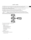
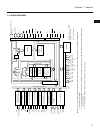
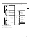
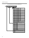
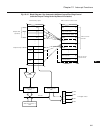
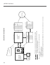
1 2 3 4 5 6 7 8 general pin functions cpu function clock generator port functions real-time output function timer/counter units a/d converter 9 asynchronous serial interface clock synchronous serial interface edge detection function local bus interface function 13 12 11 10 17 16 15 14 c b a 18 inter...
Page 3
Cautions on cmos devices 1 countermeasures against static electricity for all moss caution when handling mos devices, take care so that they are not electrostatically charged. Strong static electricity may cause dielectric breakdown in gates. When transporting or storing mos devices, use conductive ...
Page 4
The information in this document is subject to change without notice. No part of this document may be copied or reproduced in any form or by any means without the prior written consent of nec corporation. Nec corporation assumes no responsibility for any errors which may appear in this document. Nec...
Page 5
Main revisions in this edition page description p.55 v ss and "caution" have been added in (a) of fig. 4-2. P.329 "caution" has been added in (2) of section 12.4.6. P.383 "caution" has been added in (b) of section 14.4.2. P.429 appendix b has been modified as follows: • "ibm pc series" has been chan...
Page 6
Preface users: this manual is aimed at engineers who need to be familiar with the capabilities of the µpd78214 sub-series for application program development purposes. Purpose: the purpose of this manual is to help users understand the hardware capabilities of the µpd78214 sub-series. Organization: ...
Page 7
Pd78p214 pd78p214(a) µ µ pd78214 pd78214(a) µ µ pd78213 pd78213(a) µ µ pd78212 pd78212(a) µ µ prom 16k ram 512 rom 16k ram 512 rom-less ram 512 rom 8k ram 384 to check the details of a register when you know the name of the register: see appendix d. To check the differences between the µpd78214 sub-...
Page 8
Never use the code combinations indicated "not to be set" in the register descriptions. Characters likely to be confused: 0 (zero) and o (uppercase "o") 1 (one), l (lowercase "l"), and i (uppercase "i") related documents: the following reference documents are also available. • documents related to t...
Page 9
• documents related to development tools ie-78210-r in-circuit emulator system software operator's manual cc78k series c compiler user's manual document no. Eeu-1395 eeu-1322 eeu-1331 eep-1027 eem-1024 eem-1260 eem-1027 eeu-1283 eeu-1273 eeu-1254 eeu-1289 eeu-1280 eeu-1447 eeu-1413 ef-1114 document ...
Page 10
• other documents document no. Iei-1213 iei-1207 iei-1209 iei-1203 mei-1202 document name package manual smd surface mount technology manual quality grades on nec semiconductor devices nec semiconductor device reliability/quality control system guide to quality assurance for semiconductor devices ca...
Page 12
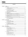
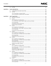
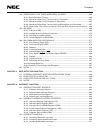
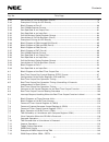
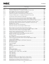
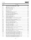
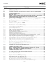
- i - contents contents chapter 1 general ........................................................................................................................................1 1.1 features ..............................................................................................................
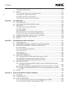
Page 13
- ii - contents 3.3 notes ...................................................................................................................................53 chapter 4 clock generator .....................................................................................................................
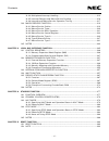
Page 14
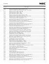
- iii - contents preface 5.8.4 built-in pull-up resistor ..........................................................................................93 5.8.5 notes .........................................................................................................................93 5.9 notes .......
Page 15
- iv - contents 7.4.6 sample applications ..................................................................................................211 7.5 notes ...................................................................................................................................212 7.5.1 commo...
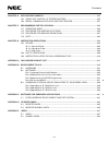
Page 16
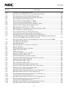
- v - contents 10.4 operations in the three-wire serial i/o mode .................................................. 265 10.4.1 basic operation timing ..........................................................................................265 10.4.2 operation when only transmission is permitted ......
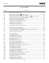
Page 17
- vi - contents 12.3.4 multiplexed-interrupt handling ..............................................................................313 12.3.5 interrupt request and macro service pending ....................................................316 12.3.6 interrupt and macro service operation timing ........
Page 18
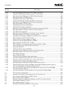
- vii - contents chapter 16 application examples ............................................................................................................395 16.1 open-loop control of stepper motors ..............................................................395 16.2 serial communication with m...
Page 19
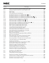
- viii - contents list of figures fig. No. Title, page 2-1 i/o circuits provided for pins .......................................................................................................34 3-1 memory map of µpd78212 (ea pin driven high) ...........................................................
Page 20
- ix - contents fig. No. Title, page 5-25 connection of pull-up resistors (port 4) ...................................................................................79 5-26 example of driving an led directly ..............................................................................................
Page 21
- x - contents fig. No. Title, page 7-16 example of rewriting compare register cr00 .........................................................................124 7-17 example of pwm output signal with a 100% duty factor ......................................................124 7-18 example of ppg out...
Page 22
- xi - contents 7-62 timing of pulse width measurement .........................................................................................156 7-63 setting of control registers for pulse width measurement ...................................................157 7-64 setting procedure for pulse wi...
Page 23
- xii - contents 7-106 interrupt request handling for pulse width calculation .........................................................197 7-107 example of pwm signal output by 8-bit timer/counter 2 ..................................................... 197 7-108 setting of control registers for pwm ...
Page 24
- xiii - contents 8-9 software-started scan-mode a/d conversion ..........................................................................235 8-10 example of malfunction in a hardware-started a/d conversion ........................................... 236 8-11 select-mode a/d conversion started by ha...
Page 25
- xiv - contents 11-1 format of external interrupt mode register 0 (intm0) ...........................................................294 11-2 format of external interrupt mode register 1 (intm1) ...........................................................295 11-3 edge detection on pin p20 .............
Page 26
- xv - contents 13-1 format of the memory expansion mode register (mm) .........................................................346 13-2 format of programmable wait control register (pw) .............................................................347 13-3 read timing ..................................
Page 27
- xvi - contents 17-1 timing chart for prom write and verify .................................................................................. 400 17-2 write operation flowchart ...........................................................................................................401 17-3 prom ...
Page 28
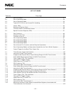
- xvii - contents list of tables table no. Title, page 2-1 port 2 functions .............................................................................................................................27 2-2 port 3 operating mode .........................................................................
Page 29
- xviii - contents 8-1 modes generating the intad ......................................................................................................225 8-2 a/d conversion time ....................................................................................................................232 ...
Page 30
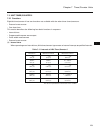
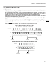
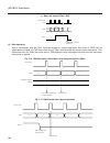
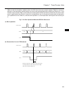
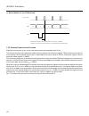
1 1 chapter 1 general the µpd78214 sub-series is part of the 78k/ii series of eight-bit single-chip microcomputers capable of accessing an expanded memory space of 1 megabyte. This sub-series consists of the following products. The µpd78214 offers a 16-kb masked rom, 512-byte ram, highly functional ...
Page 31
2 µ pd78214 sub-series 78k/ii products the following are contained: a /d converter d/a converter the pwm output function is added. The macro service and timer/ counter are enhanced. The comparator is deleted. Pd78234 sub-seriesµ the d/a converter is contained. The pwm output function is added. The m...
Page 32
3 chapter 1 general 1 1.1 features ° 78k/ii series ° multiplexed internal bus (faster execution of instructions) minimum instruction cycle (operating at 12 mhz): 333 ns ( µpd78212, µpd78214, and µpd78p214), or 500 ns ( µpd78213) ° instruction set suitable for control applications ° data memory expan...
Page 33
4 µ pd78214 sub-series 1.2 ordering information and quality grade 1.2.1 ordering information ordering code package internal rom µpd78212cw-××× 64-pin plastic shrink dip (750 mil) masked rom µpd78212gc-×××-ab8 64-pin plastic qfp (14 × 14 mm) masked rom µpd78212gj-×××-5bj 74-pin plastic qfp (20 × 20 m...
Page 34
5 chapter 1 general 1 1.2.2 quality grade ordering code package quality grade µpd78212cw-××× 64-pin plastic shrink dip (750 mil) standard µpd78212gc-×××-ab8 64-pin plastic qfp (14 × 14 mm) standard µpd78212gj-×××-5bj 74-pin plastic qfp (20 × 20 mm) standard µpd78213cw 64-pin plastic shrink dip (750 ...
Page 35
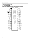
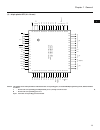
6 µ pd78214 sub-series 1.3 pin configuration (top view) 1.3.1 normal operating mode (1) 64-pin plastic shrink dip, 64-pin plastic quip, 64-pin ceramic shrink dip with window 1 2 3 4 5 6 7 8 9 10 11 12 13 14 15 16 17 18 19 20 21 22 23 24 25 26 27 28 29 30 31 32 p02 p01 p00 p37/to3 p36/to2 p35/to1 p34...
Page 36
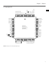
7 chapter 1 general 1 (2) 68-pin plastic qfj remark the nc pin is not connected inside the chip. 10 11 12 13 14 15 16 17 18 19 20 21 22 23 24 25 26 p70/an0 p34/to0 p35/to1 p36/to2 p37/to3 p00 p01 p02 p03 p04 p05 p06 p07 nc p67/refrq/an7 p66/wait/an6 p65/wr 60 59 58 57 56 55 54 53 52 51 50 49 48 47 4...
Page 37
8 µ pd78214 sub-series (3) 64-pin plastic qfp (14 × 14 mm) 1 2 3 4 5 6 7 8 9 10 11 12 13 14 15 16 p64/rd p63/a19 p62/a18 p61/a17 p60/a16 reset x2 x1 v ss p57/a15 p56/a14 p55/a13 p54/a12 p53/a11 p52/a10 p51/a9 p71/an1 p72/an2 p73/an3 p74/an4 p75/an5 av ref av ss v dd ea p33/so/sb0 p32/sck p31/t x d p...
Page 38
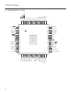
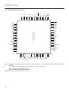
9 chapter 1 general 1 (4) 74-pin plastic qfp (20 × 20 mm) remark the nc pins are not connected inside the chip. P65/wr p66/wait/an6 p67/refrq/an7 p07 nc p06 p05 p04 p03 nc p02 p01 p00 p37/to3 p36/to2 p35/to1 nc p34/to0 p70/an0 56 55 54 53 52 51 50 49 48 47 46 45 44 43 42 41 40 39 38 1 2 3 4 5 6 7 8 ...
Page 39
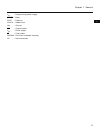
10 µ pd78214 sub-series p00-p07 : port 0 p20-p27 : port 2 p30-p37 : port 3 p40-p47 : port 4 p50-p57 : port 5 p60-p67 : port 6 p70-p75 : port 7 to0-to3 : timer output ci : clock input rxd : receive data txd : transmit data sck : serial clock asck : asynchronous serial clock sbo : serial bus si : seri...
Page 40
11 chapter 1 general 1 1.3.2 prom programming mode (p20/nmi = 12.5 v, reset = l) (1) 64-pin plastic shrink dip, 64-pin plastic quip, 64-pin ceramic shrink dip with window caution the symbols enclosed in parentheses indicate that the corresponding pins, not used in prom programming mode, shall be han...
Page 41
12 µ pd78214 sub-series (2) 68-pin plastic qfj caution the symbols enclosed in parentheses indicate that the corresponding pins, not used in prom programming mode, shall be handled as follows: l : connect the corresponding pin independently to v ss , through a 10-k Ω resistor. G : connect the corres...
Page 42
13 chapter 1 general 1 (3) 64-pin plastic qfp (14 × 14 mm) caution the symbols enclosed in parentheses indicate that the corresponding pins, not used in prom programming mode, shall be handled as follows: l : connect the corresponding pin independently to v ss , through a 10-k Ω resistor. G : connec...
Page 43
14 µ pd78214 sub-series (4) 74-pin plastic qfp (20 × 20 mm) caution the symbols enclosed in parentheses indicate that the corresponding pins, not used in prom programming mode, shall be handled as follows: l : connect the corresponding pin independently to v ss , through a 10-k Ω resistor. G : conne...
Page 44
15 chapter 1 general 1 v pp : programming power supply reset : reset d0-d7 : data bus a0-a14 : address bus v ss : ground oe : output enable v dd : power supply ce : chip enable p20/nmi : port 2/non-maskable interrupt nc : non-connection.
Page 45
16 µ pd78214 sub-series 1.4 example application system (printer) m p00-p03 m p04-p07 to sck so t x d r x d ports av ref av ss an0 an1 an2-an7 temperature sensor motor supply voltage sw input for each mode reset x1 x2 v ss v dd a8-a15 astb ad0-ad7 refrq wr rd a16-a19 pd78214 µ decoder latch data bus ...
Page 46
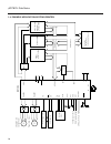
17 chapter 1 general 1 1.5 block diagram notes 1. None for µ pd78213 and µ pd78213(a), 8kb for µ pd78212 and µ pd78212(a), 16kb for µ pd78214, µ pd78p214, µ pd78214(a) 2. Internal dual-port ram 3. Peripheral ram (pram). 128 bytes for µ pd78212 and µ pd78212(a), 256 bytes for µ pd78213, µ pd78214, µ ...
Page 47
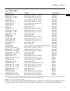
18 µ pd78214 sub-series 1.6 functions item input pins output pins i/o pins total connected to a pull-up resistor driving a led directly driving a transistor directly 65 µpd78213 µpd78212 µpd78214 µpd78p214 real-time output ports general-purpose registers timer/counters 333 ns 500 ns 8k bytes 16k byt...
Page 48
19 chapter 1 general 1 item a/d converter interrupt instruction set package µpd78213 µpd78212 µpd78214 µpd78p214 eight channels, each having a resolution of eight bits • 19 interrupts (seven external and 12 internal) plus those caused by brk instructions • two programmable priority levels • two type...
Page 49
20 µ pd78214 sub-series product item ram capacity i/o pins timer/counter serial interface interrupt a/d converter package others µpd78213 512 bytes • software programmable pull-up resistors: supported • transistor direct drive outputs: supported pwm/ppg output: supported scaler for the baud rate gen...
Page 50
21 chapter 1 general 1 series name µpd78214 sub-series µpd78218a sub-series µpd78214 µpd78214(a) µpd78218a product µpd78212 µpd78212(a) µpd78213 µpd78213(a) µpd78p214 µpd78p214(a) µ pd78217a µpd78p218a minimum instruction cycle (when operating at 12 mhz) 333 ns 500 ns 333 ns 333 ns 500 ns operating ...
Page 51
22 µ pd78214 sub-series product item quality grade package standard • 64-pin plastoc shrink dip • 64-pin plastic qfp • 74-pin plastic qfp µpd78212 µpd78212(a) special • 64-pin plastoc shrink dip • 64-pin plastic qfp product item quality grade maximum period in which 74- pin plastic qfps can be solde...
Page 52
23 chapter 1 general 1 product name parameter internal rom internal ram port 4 port 5 port 6 others 8kb masked rom at 00000h to 01fffh 384 bytes at 0fd80h to 0feffh used as both general-purpose i/o port (p40 to p47) and address/data bus (ad0 to ad7) used as both general-purpose i/o port (p50 to p57)...
Page 53
24.
Page 54
25 2 chapter 2 pin functions 2.1 pin function list 2.1.1 normal operating mode (1) ports p20 p21 p22 p23 p24 p25 p26 p27 p30 p31 p32 p33 p34-p37 p60-p63 p64 note 2 p65 note 2 p66 p67 p70-p75 port 0 (p0): can be used as two four-bit, real-time output ports. Can drive transistors directly. Port 2 (p2)...
Page 55
26 µ pd78214 sub-series (2) pins other than those which function as ports to0-to3 ci rxd txd asck sb0 si so sck nmi intp0 intp1 intp2 intp3 intp4 intp5 ad0-ad7 a8-a15 a16-a19 rd wr wait astb refrq reset x1 x2 an0-an5 an6, an7 av ref av ss v dd v ss nc p34-p37 p23/intp2 p30 p31 p25/intp4 p33/so p27 p...
Page 56
27 chapter 2 pin functions 2 2.1.2 prom programming mode (only for the µpd78p214, p20/nmi = 12.5 v, reset = l) pin p20/nmi reset a0-a14 d0-d7 ce oe v pp v dd v ss nc function address bus data bus prom enable input read strobe to prom power for programming main power ground — input input/output input...
Page 57
28 µ pd78214 sub-series (a) when functioning as a port signals applied to these pins can be read and these pins can be tested, regardless of whether these pins are acting as secondary function pins. (b) when functioning as control-signal input pins (i) nmi (non-maskable interrupt) apply an external ...
Page 58
29 chapter 2 pin functions 2 table 2-2 port 3 operating mode (n = 0 to 7) p30 p31 p32 p33 p34 p35 p36 p37 rxd input txd output sck input/output so output/sb0 input/output to0 output to1 output to2 output to3 output mode pmc3 setting port mode pmc3n = 0 control signal i/o mode pmc3n = 1 i/o port (a) ...
Page 59
30 µ pd78214 sub-series (6) p60 to p67 (port 6): output (p60 to p63) and tristate inputs/outputs (p64 to p67) port 6 is an eight-bit i/o port with output latches. Pins p64 to p67 are provided with software-programmable pull-up resistors. The pins of port 6 also function as control signal input pins,...
Page 60
31 chapter 2 pin functions 2 (8) astb (address strobe): output timing signal output used for latching addresses externally to enable access to external memory. (9) ea (external access): input control signal input used for switching the program memory from the internal rom to the external memory. Whe...
Page 61
32 µ pd78214 sub-series (9) v ss ground. (10) nc (non-connection) not connected inside the chip..
Page 62
33 chapter 2 pin functions 2 2.3 i/o circuits and unused-pin handling table 2-4 lists the types of i/o circuits provided for each pin and describes how pins are handled when not used. Fig. 2-1 illustrates the i/o circuit types. Table 2-4 types of i/o circuits and unused-pin handling p00-p07 p20/nmi ...
Page 63
34 µ pd78214 sub-series fig. 2-1 i/o circuits provided for pins type 1 in v dd p n type 2 in schmitt trigger input with hysteresis characteristics type 4 data v dd p n out output disable push-pull output which can output high impedance (both the positive and negative channels are off.) type 8-a data...
Page 64
35 chapter 2 pin functions 2 2.4 notes (1) while the reset signal is being applied, pins p60 to p63 are high impedance. When the reset signal is released, the output of these pins is low level. Design the peripheral circuit so that it operates satisfactorily when pins p60 to p63 initially output the...
Page 65
36.
Page 66
37 3 chapter 3 cpu function 3.1 memory space the µpd78214 can access a memory space of up to 1m byte. Figs. 3-1 to 3-4 show the corresponding memory maps. The mapping of program memory depends on the status of the ea pin. The ea pin of the µpd78213 must be tied low. (1) µpd78212 program memory is ma...
Page 67
38 µ pd78214 sub-series fig. 3-1 memory map of µpd78212 (ea pin driven high) notes 1. Accessed in 1m-byte expansion mode. 2. External sfr area remark the shaded areas indicate internal memory. Fffffh 10000h 0ffffh 0ffdfh 0ffd0h 0ff00h 0feffh 0fd80h 0fd7fh 02000h 01fffh 00000h data memory expansion a...
Page 68
39 chapter 3 cpu function 3 fig. 3-2 memory map of µpd78212 (ea pin driven low) notes 1. Accessed in 1m-byte expansion mode. 2. External sfr area remark the shaded areas indicate internal memory. Fffffh 10000h 0ffffh 0ffdfh 0ffd0h 0ff00h 0feffh 0fd80h 0fd7fh 00000h data memory expansion address data...
Page 69
40 µ pd78214 sub-series fig. 3-3 memory map of µpd78213, µpd78214, or µpd78p214 (ea pin driven low) notes 1. Accessed in 1m-byte expansion mode. 2. External sfr area remark the shaded areas indicate internal memory. Fffffh 10000h 0ffffh 0ffdfh 0ffd0h 0ff00h 0feffh 0fd00h 0fcffh 00000h data memory ex...
Page 70
41 chapter 3 cpu function 3 fig. 3-4 memory map of µpd78214, µpd78p214 (ea pin driven high) notes 1. Accessed in 1m-byte expansion mode. 2. Accessed in external memory expansion mode 3. External sfr area remark the shaded areas indicate internal memory. Fffffh 10000h 0ffffh 0ffdfh 0ffd0h 0ff00h 0fef...
Page 71
42 µ pd78214 sub-series 3.1.1 internal program memory area in the area from 00000h to 03fffh (00000h to 01fffh for the µpd78212), a 16k × 8 bit rom (8k × 8 bit rom for the µpd78212) is incorporated. Programs and table data are stored in this area. Usually, the program counter (pc) is used for addres...
Page 72
43 chapter 3 cpu function 3 3.1.2 internal ram area a 512-byte (384-byte for the µpd78212) general-purpose static ram is incorporated into the area from 0fd00h to 0feffh. This area consists of the following two rams: ° peripheral ram (pram) : 0fd00h to 0fdffh (0fd80h to 0fdffh for the µpd78212) ° in...
Page 73
44 µ pd78214 sub-series to access the space, specify the bank to be used (high-order four bits of address, a16 to a19) in the bank register (p60 to p63 of register p6, or pm60 to pm63 of register pm6). Then, execute an instruction which allows extended addressing. The high-order four bits of address...
Page 74
45 chapter 3 cpu function 3 3.2 registers 3.2.1 program counter (pc) this 16-bit binary counter holds the address of the program to be executed next (see fig. 3-6). Usually, the address is automatically incremented according to the number of bytes of the instruction to be fetched. If an instruction ...
Page 75
46 µ pd78214 sub-series (3) register bank selection flags (rbs0, rbs1) these two flags are used to select one of four register banks (see table 3-2). The flags hold two-bit information indicating the register bank selected by the sel rbn instruction. Table 3-2 selecting a register bank 0 0 1 1 regis...
Page 76
47 chapter 3 cpu function 3 fig. 3-9 data saved to the stack area fig. 3-10 data restored from the stack area push rp instruction stack register pair, low register pair, high sp – 2 sp – 1 sp ⇒ sp ← sp – 2 ↑ ↑ call, callf, and callt instructions stack pc7-pc0 pc15-pc8 sp – 2 sp – 1 sp ⇒ sp ← sp – 2 ...
Page 77
48 µ pd78214 sub-series fig. 3-11 configuration of general-purpose registers a e1h b e3h d e5h h e7h a e9h b ebh d edh h efh a f1h b f3h d f5h h f7h a f9h b fbh d fdh h ffh x e0h c e2h e e4h l e6h x e8h c eah e ech l eeh x f0h c f2h e f4h l f6h x f8h c fah e fch l feh ax bc de hl ax bc de hl ax bc d...
Page 78
49 chapter 3 cpu function 3 (2) function general-purpose registers can be operated in units of eight bits. They can also be operated in units of 16 bits, that is, a pair of eight-bit registers can be operated as a single unit (ax, bc, de, hl). Each register can temporarily hold operation results or ...
Page 79
50 µ pd78214 sub-series 3.2.5 special function registers (sfr) a mode register, control register, and other registers with special functions, which are built-in hardware peripherals, are mapped into the 256-byte space from 0ff00h to 0ffffh. Caution never access an address to which no sfr is mapped i...
Page 80
51 chapter 3 cpu function 3 0ff00h 0ff02h 0ff03h 0ff04h 0ff05h 0ff06h 0ff07h 0ff0ah 0ff0bh 0ff0ch 0ff10h 0ff11h 0ff12h 0ff13h 0ff14h 0ff15h 0ff16h 0ff17h 0ff18h 0ff19h 0ff1ah 0ff1ch 0ff20h 0ff23h 0ff25h 0ff26h 0ff30h 0ff31h 0ff32h 0ff34h 0ff40h 0ff43h 16 bits 8 bits 1 bit p0 p2 p3 p4 p5 p6 p7 p0l p0...
Page 81
52 µ pd78214 sub-series 0ff50h 0ff51h 0ff52h 0ff54h 0ff56h 0ff5ch 0ff5dh 0ff5eh 0ff5fh 0ff68h 0ff6ah 0ff80h 0ff82h 0ff86h 0ff88h 0ff8ah 0ff8ch 0ff8eh 0ff90h 0ffc0h 0ffc4h 0ffc5h 0ffc6h 0ffd0h 0ffdfh 0ffe0h 0ffe1h 0ffe4h 0ffe5h 0ffe8h 0ffe9h 0ffech 0ffedh 0fff4h 0fff5h 0fff8h tm1 tm2 tm3 prm0 tmc0 pr...
Page 82
53 chapter 3 cpu function 3 3.3 notes (1) a program fetch from the internal ram area is prohibited. (2) operation of the stack pointer in stack addressing, the entire 64k bytes can be accessed. No stack area can be mapped into the sfr area or internal rom area. (3) special function register (sfr) ne...
Page 83
54.
Page 84
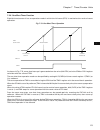
55 4 chapter 4 clock generator 4.1 configuration and function a clock generator generates and controls the internal system clock (clk) sent to the cpu. Fig. 4-1 shows the configuration of the clock generator. Fig. 4-1 block diagram of clock generator remarks f xx : crystal/ceramic oscillation freque...
Page 85
56 µ pd78214 sub-series remark different uses of the crystal and ceramic resonator generally, a crystal’s oscillation frequency is quite stable. Crystals are ideal for high-precision time management (for example, clock or frequency measurement). In comparison with crystals, ceramic resonators are le...
Page 86
57 chapter 4 clock generator 4 fig. 4-4 notes on connection of the oscillator x2 pd78214 µ x1 v ss cautions 1. Place the oscillator as close as possible to pins x1 and x2. 2. Do not let other signal lines cross the circuit enclosed in a dashed line. Fig. 4-5 incorrect oscillator connections (a) the ...
Page 87
58 µ pd78214 sub-series (c) a varying high current flows too close to the signal line. (d) a current flows through the ground line of the oscillator. (the potentials vary at points a, b, and c.) (e) a signal is being drawn from the oscillator. (2) at power-on or return from stop mode, some time is r...
Page 88
59 5 chapter 5 port functions 5.1 digital i/o ports the µpd78214 has the ports shown in fig. 5-1. These ports can be used for various types of control. Table 5-1 lists the function of each port. For ports 2 through 6, software can specify whether to use a built-in pull-up resistor for inputs. Fig. 5...
Page 89
60 µ pd78214 sub-series table 5-1 port functions port 0 port 2 port 3 port 4 note port 5 note port 6 note port 7 software-specified pull-up resistor name pin name p00-p07 p20-p27 p30-p37 p40-p47 p50-p57 p60-p63 p64-p67 p70-p75 function can be specified for either output in 8-bit units or high impeda...
Page 90
61 chapter 5 port functions 5 5.2.1 hardware configuration fig. 5-2 shows the hardware configuration of port 0. Fig. 5-2 configuration of port 0 5.2.2 setting the input/output mode and control mode the port 0 mode register (pm0) sets the i/o mode of port 0, as shown in fig. 5-3. This register is set...
Page 91
62 µ pd78214 sub-series 5.2.3 operation port 0 is an output-only port. Once port 0 is put in the output mode, the output latch becomes operable, enabling data transfer between the output latch and accumulator according to a transfer instruction. The output latch can be loaded with any data by a logi...
Page 92
63 chapter 5 port functions 5 5.3 port 2 port 2 is an 8-bit input-only port. P22 through p27 have a software-programmable built-in pull-up resistor. In addition to functioning as an input port, port 2 functions as a control signal input pin such as for external interrupts (see table 5-3). All the 8 ...
Page 93
64 µ pd78214 sub-series 5.3.1 hardware configuration fig. 5-6 shows the configuration of port 2 fig. 5-6 block diagram of port 2 note p20 or p21 does not have a circuit enclosed in a dotted box. 5.3.2 setting the input mode and control mode port 2 is an input-only port. There is no register to speci...
Page 94
65 chapter 5 port functions 5 fig. 5-7 port specified as an input port caution for the in-circuit emulator, the level of each port 2 pin from which noise has not been removed can be read and tested. 5.3.4 built-in pull-up resistor p22 through p27 have built-in pull-up resistors. When they must be pu...
Page 95
66 µ pd78214 sub-series fig. 5-9 connection of pull-up resistors (port 2) caution p22 through p26 are not pulled up immediately after a reset. In this case, intp1 through intp5 (one of the multiple functions assigned to p22 to p26) may set interrupt request flags. To avoid this problem, specify use ...
Page 96
67 chapter 5 port functions 5 table 5-4 port 3 operating modes (n = 0 through 7) condition p30 p31 p32 p33 p34 p35 p36 p37 mode control signal i/o mode pmc3n = 1 rxd input txd output sck i/o so output or sb0 i/o to0 output to1 output to2 output to3 output port mode pmc3n = 0 i/o port (a) port mode i...
Page 97
68 µ pd78214 sub-series 5.4.1 hardware configuration fig. 5-10 through 5-13 show the configuration of port 3. Fig. 5-10 block diagram of p30 (port 3) p30 internal bus wr pm30 port 3 mode register pm30 wr pmc30 pmc30 wr p30 p30 rd puo wr puo rd pmc30 rd p30 rd p30 rxd input puo3 pull-up resistor opti...
Page 98
69 chapter 5 port functions 5 fig. 5-11 block diagram of p31, and p34 through p37 (port 3) internal bus rd puo wr puo wr pm3n port 3 mode register pm3n wr pmc3n pmc3n wr p3n p3n rd pmc3n rd p3n pull-up resistor option register puo3 p3n n = 1, 4, 5, 6, 7 v dd to, txd output rd p3n selector output lat...
Page 99
70 µ pd78214 sub-series fig. 5-12 block diagram of p32 (port 3) ★ internal bus rd p32 p32 rd puo wr puo pull-up resistor option register puo3 wr pm32 port 3 mode register pm32 wr pmc32 pmc32 rd pmc32 wr p32 p32 selector rd p32 sck output external sck v dd sck input output latch.
Page 100
71 chapter 5 port functions 5 fig. 5-13 block diagram of p33 (port 3) ★ 5.4.2 setting the i/o mode and control mode the port 3 mode register (pm3) can put each pin of port 3 in either the input or output mode independently of the other pins, as shown in fig. 5-14. The pm3 register is loaded with dat...
Page 101
72 µ pd78214 sub-series fig. 5-14 port 3 mode register format fig. 5-15 port 3 mode control register (pmc3) format pm37 7 pm36 6 pm35 5 pm34 4 pm33 3 pm32 2 pm31 1 pm30 0 pm3 pm3n input mode (output buffer off) output mode (output buffer on) specifies i/o mode of pin pm3n (n = 0 to 7) (ffh when rese...
Page 102
73 chapter 5 port functions 5 5.4.3 operation port 3 is an i/o port. Its pins also function as control signal pins. (1) output port when port 3 is in the output mode, its output latch is operable. Once the output latch becomes operable, data can be transferred between the output latch and the accumu...
Page 103
74 µ pd78214 sub-series (3) control signal input or output regardless of setting of the port mode 3 register (pm3), each bit of port 3 can be used to input or output a control signal, independently of the other bits, by setting the corresponding bit of the port mode control register (pmc3) to 1. Whe...
Page 104
75 chapter 5 port functions 5 fig. 5-20 connection of pull-up resistors (port 3) 5.5 port 4 port 4 is an 8-bit i/o port with an output latch. The memory expansion mode register (mm) can put all 8 bits of this port in either the input or output mode at one time. Each pin has a software-programmable b...
Page 105
76 µ pd78214 sub-series 5.5.1 hardware configuration fig. 5-21 shows the hardware configuration of port 4. Fig. 5-21 block diagram of port 4 5.5.2 setting the i/o mode and control mode the memory expansion mode register (mm, see fig 13-1) specifies the operating mode of port 4, as listed in table 5-...
Page 106
77 chapter 5 port functions 5 5.5.3 operation port 4 is an i/o port. It functions also as an address/data bus (ad0 through ad7). (1) output port when port 4 is in the output mode, its output latch is operable. Once the output latch becomes operable, data can be transferred between the output latch a...
Page 107
78 µ pd78214 sub-series (3) address/data bus (ad0 through ad7) port 4 is used as the address/data automatically for external access. Do not execute i/o instructions for port 4. 5.5.4 built-in pull-up resistor port 4 has built-in pull-up resistors. When port 4 must be pulled up, the built-in pull-up ...
Page 108
79 chapter 5 port functions 5 fig. 5-25 connection of pull-up resistors (port 4) 5.5.5 driving leds directly for port 4, the low level side of the output buffer has an enhanced driving capacity so that it can drive an led directly on an active-low signal. Fig. 5-26 is an example of such an output bu...
Page 109
80 µ pd78214 sub-series 5.6 port 5 port 5 is an 8-bit i/o port with an output latch. The port 5 mode register (pm5) can put each bit of this port in either the input or output mode, independently of the other bits. Each pin has a software-programmable built-in pull- up resistor, and can drive an led...
Page 110
81 chapter 5 port functions 5 fig. 5-28 port 5 mode register format table 5-6 port 5 operating modes 1 1 0 0 1 × mm2 0 1 × mm1 × 1 × mm0 ea pin mm register bit operation mode i/o port address/data bus (a8-a15) for the µpd78213, port 4 functions only as the address/data bus (ad8 through ad15). 5.6.3 ...
Page 111
82 µ pd78214 sub-series fig. 5-30 port specified as an input port caution although its ultimate purpose is to manipulate only 1 bit, a bit manipulation instruction accesses a port in 8-bit units. If a bit manipulation instruction is used for a port some pins of which are in the output mode and the o...
Page 112
83 chapter 5 port functions 5 fig. 5-32 connection of pull-up resistors (port 5) 5.6.5 driving leds directly for port 5, the low level side of the output buffer has an enhanced driving capacity so that it can drive an led directly on an active-low signal. Fig. 5-33 is an example of such an output bu...
Page 113
84 µ pd78214 sub-series 5.7 port 6 port 6 is an 8-bit i/o port with an output latch. P64 through p67 have a software-programmable built-in pull-up resistor. In addition to the port functions, port 5 works as i/o pins for various control signals as listed in table 5-7. Each control pin is operated by...
Page 114
85 chapter 5 port functions 5 (vi) an6 and an7 (analog input) these pins receive analog signals for the a/d converter. 5.7.1 hardware configuration fig. 5-34 through 5-37 show the hardware configuration of port 6. Fig. 5-34 block diagram of p60 through p63 (port 6) p6n n = 0, 1, 2, 3 wr mm6 memory e...
Page 115
86 µ pd78214 sub-series fig. 5-35 block diagram of p64 and p65 (port 6) internal bus p64 (p65) v dd rd in selector rd puo wr puo pull-up resistor option register puo6 port 6 mode register p64 (p65) wr pm64, pm65 output latch pm64 (pm65) wr p64, p65 ea external extended mode rd signal (wr signal) rd ...
Page 116
87 chapter 5 port functions 5 fig. 5-36 block diagram of p66 (port 6) internal bus p66 v dd rd in rd puo wr puo pull-up resistor option register puo6 port 6 mode register pm66 wr pm66 output latch wr p66 rd out external wait specification p66 wait input a/d converter.
Page 117
88 µ pd78214 sub-series fig. 5-37 block diagram of p67 (port 6) 5.7.2 setting the i/o mode and control mode the port 6 mode register (pm6) can put port 6 in either the input or output mode as shown in fig. 5-38. Table 5- 8 lists the operations needed to make port 6 function as control pins. P66 and ...
Page 118
89 chapter 5 port functions 5 cautions 1. To use p60 through p63 as an output port, it is necessary to reset the pm60 through pm63 bits to 0. If they are not 0, the in- circuit emulator may not work. 2. To use the p66/wait pin as the wait pin, it is necessary to put p66 in the input mode using the p...
Page 119
90 µ pd78214 sub-series 5.7.3 operation port 6 is an i/o port. Its pins also function as control signal pins. (1) output port when port 6 is in the output mode, the contents of its output latch are output, and data can be transferred between the output latch and the accumulator using a transfer inst...
Page 120
91 chapter 5 port functions 5 (3) control pins when port 6 function as control pins, they cannot be manipulated or tested by software. (4) analog inputs (p66 and p67 only) when port 6 is used as analog input pins (an6 and an7), the level of each pin can be read and tested. 5.7.4 built-in pull-up res...
Page 121
92 µ pd78214 sub-series 5.7.5 note when p66 and p67 are used as analog input pins an6 and an7 respectively or when a/d conversion is not performed, do not apply a voltage out of the range av ss through av ref to these pins, if an6 and an7 are selected for ani0 through ani2 of the a/d converter mode ...
Page 122
93 chapter 5 port functions 5 5.8.3 operation port 7 is an input-only port, and the level of its pins can be read and tested. Fig. 5-44 port specified as an input port internal bus rd in p7n n = 0 to 5 5.8.4 built-in pull-up resistor port 0 has no built-in pull-up resistor. 5.8.5 notes (1) when p70 ...
Page 123
94 µ pd78214 sub-series (4) p22 through p26 are not pulled up immediately after a reset, and the interrupt request flag may be set depending on the function of a dual-function pin (intp1 through intp5). Therefore, specify connection of a pull-up resistor in the initialization routine, before clearin...
Page 124
95 6 chapter 6 real-time output function 6.1 configuration and function the real-time output function is implemented by the hardware centering around port 0 and the buffer register (p0h and p0l) as shown in fig. 6-1. The term real-time output function refers to a function that transfers data in the ...
Page 125
96 µ pd78214 sub-series fig. 6-1 block diagram of the real-time output port 4 4 4 p00 p01 p02 p03 p04 p05 p06 p07 intp0 p0ml intc10 selector selector p0mh p0ml extr p0mh byte intc11 4 p0l p0h buffer register 8 output latch p0 4-bit real-time output (p0h) 4-bit real-time output (p0l) 8-bit real-time ...
Page 126
97 chapter 6 real-time output function 6 6.2 real-time output control register (rtpc) the real-time output control register (rtpc) is an 8-bit register to specify the functions of port 0. An 8-bit manipulation instruction and a bit manipulation instruction can be used to read data from and write dat...
Page 127
98 µ pd78214 sub-series table 6-1 port 0 operating modes and operations needed for the port 0 buffer registers 8-bit port mode 8-bit real-time output port mode 4-bit separate real-time output port mode p00-p03: port p04-p07: real-time output port mode p00-p03: real-time output port mode p04-p07: por...
Page 128
99 chapter 6 real-time output function 6 6.4 operation when port 0 is in the real-time output port mode, the contents of the buffer registers (p0h and p0l) are sent to the output latches for output to the pins of port 0 in synchronization with the occurrence of a trigger condition listed in table 6-...
Page 129
100 µ pd78214 sub-series fig. 6-4 real-time output port operation timing d02 d03 d02 d01 d00 d01 d03 d04 0h cr11 cr11 cr11 cr11 ffh timer starts intc11 interrupt request cpu operation buffer register (p0h) output latches (p07-p04) 8-bit timer/ counter 1 the contents of the buffer register and compar...
Page 130
101 chapter 6 real-time output function 6 fig. 6-5 real-time output port operation timing (controlling 2 channels independently of each other) 8-bit timer/ counter 1 timer starts 0h intc11 interrupt request intc10 interrupt request cpu operation d01 d11 d00 d01 d02 d03 d04 d03 d02 d12 d13 d12 d13 d1...
Page 131
102 µ pd78214 sub-series 6.5 application example this section describes an example of application in which p00 through p03 are used as a 4-bit real-time output port. Each time tm1 for 8-bit timer/counter 1 coincides with the contents of cr10, the contents of the p0l are output to p00 through p03. At...
Page 132
103 chapter 6 real-time output function 6 fig. 6-7 contents of the control register for the real-time output function 7 6 5 4 3 2 1 0 0 0 0 0 0 0 0 1 rtpc uses pins p00 to p03 as real-time output ports disables data transfer by intp0 from the buffer register to the output latch uses pins p04 to p07 ...
Page 133
104 µ pd78214 sub-series fig. 6-9 interrupt request handling when the real-time output function is used 6.6 notes (1) when the p0ml or p0mh is set to 1, the output buffer for the corresponding output port is turned on to output the contents of the port 0 output latch, regardless of the contents of t...
Page 134
105 chapter 6 real-time output function 6 (4) with an in-circuit emulator, digital noise cannot be eliminated normally from the intp0 pin. When it is specified that data transfer from the buffer register to the output latch be performed according to a signal from the intp0 pin, data transfer may occ...
Page 135
106.
Page 136
107 7 chapter 7 timer/counter units the µpd78214 contains one 16-bit timer/counter unit (channel) and three 8-bit timer/counter units (channels). Table 7-1 timer/counter types and functions unit types and functions 16-bit timer/ counter 2 ch — — 2 ch ° ° — ° 2 — 2 ch — — — — — ° ° 2 — 2 ch ° ° 2 ch ...
Page 137
108 µ pd78214 sub-series fig. 7-1 block diagrams of timer/counter units 16-bit timer/counter unit f clk /8 timer register tm0 compare register cr00 ovf compare register cr01 capture register cr02 coinci- dence pulse output control to0 to1 intc00 intc01 intp3 edge detector intp3 8-bit timer/counter u...
Page 138
109 chapter 7 timer/counter units 7 7.1 16-bit timer/counter 7.1.1 functions the 16-bit timer/counter can function as an interval timer and can also be used for programmable square wave output and pulse width measurement. In addition to these basic functions, the 16-bit timer/counter can be used for...
Page 139
110 µ pd78214 sub-series fig. 7-2 block diagram of 16-bit timer/counter 8 clr01 compare register (cr01) 8 ento1 16 alv0 ento0 alv1 internal bus timer output control register (toc) p34/to0 p35/to1 intc01 intc00 output con- trol circuit output con- trol circuit reset mod1 mod0 pwm/ppg output control c...
Page 140
111 chapter 7 timer/counter units 7 (1) 16-bit timer 0 (tm0) tm0 is a count-up timer using a count clock of f clk /8. The count operation of tm0 can be enabled or disabled by timer control register 0 (tmc0). Tm0 allows only read operation using a 16-bit manipulation instruction. When the reset signa...
Page 141
112 µ pd78214 sub-series fig. 7-3 format of timer control register 0 (tmc0) 7 6 5 4 3 2 1 0 ce3 0 0 0 ce0 ovf0 0 0 tmc0 ovf0 0 1 1 0 ce0 tm0 overflow flag overflow does not occur overflow occurs (countiing up from ffffh to 0000h) tm0 counting control clears and stops counting enables counting these ...
Page 142
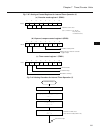
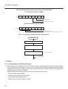
113 chapter 7 timer/counter units 7 (3) timer output control register (toc) the toc register is an 8-bit register for specifying the active level of timer output and for enabling/disabling timer output. The lower 4 bits control the timer output operation (on the to0 and to1 pins) of the 16-bit timer...
Page 143
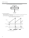
114 µ pd78214 sub-series 7.1.4 operation of 16-bit timer 0 (tm0) (1) basic operation the 16-bit timer/counter performs count operation by counting up with a count clock of f clk /8. When the reset signal is applied, tm0 is cleared to 0000h, and count operation stops. Bit 3 (ce0) of timer control reg...
Page 144
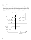
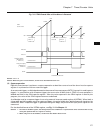
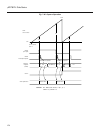
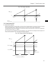
115 chapter 7 timer/counter units 7 (c) when the value of tm0 is ffffh count clock f clk /8 tm0 cleared by software ovf0 fffeh ffffh 0h 1h ovf0 ←0 (2) clear operation after a coincidence with the cr01 compare register, 16-bit timer 0 (tm0) can be automatically cleared. If a tm0 clear cause occurs, t...
Page 145
116 µ pd78214 sub-series fig. 7-8 clear operation when the ce0 bit is reset to 0 (a) basic operation tm0 ce0 n-1 n 0 count clock (b) restart after 0 is set in tm0 cleared count clock tm0 ce0 n-1 n 0 0 1 when the ce0 bit is set to 1 after this count clock, counting starts from 0 on the count clock in...
Page 146
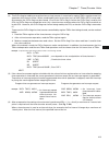
117 chapter 7 timer/counter units 7 7.1.5 compare register and capture register operations (1) compare operation the 16-bit timer/counter performs an operation to compare the values set in the compare registers with timer count values. When the values set in the compare registers (cr00, cr01) coinci...
Page 147
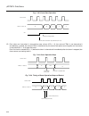
118 µ pd78214 sub-series fig. 7-10 tm0 cleared after a coincidence is detected remark clr01 = 1 (2) capture operation the 16-bit timer/counter performs a capture operation to load the count value of the timer into the capture register in synchronism with an external trigger. As an external trigger, ...
Page 148
119 chapter 7 timer/counter units 7 fig. 7-11 capture operation remark dn: tm0 count value (n = 0, 1, 2, ...) clr01 = 0 caution with an in-circuit emulator, digital noise on the intp3 pin cannot be removed correctly. When the capture function is used, the operation described below is performed if an...
Page 149
120 µ pd78214 sub-series table 7-5 timer output (to0, to1) operation toc 0 0 1 1 0 1 1 0 1 1 0 1 1 ento1 0/1 0/1 0/1 0/1 0/1 0/1 0/1 0/1 0/1 0/1 0/1 0/1 0/1 al v1 0 1 0 1 1 0 1 1 0 1 1 0 1 ento0 0/1 0/1 0/1 0/1 0/1 0/1 0/1 0/1 0/1 0/1 0/1 0/1 0/1 al v0 × 0 0 0 0 0 0 1 1 1 1 1 1 mod1 × 0 0 0 1 1 1 0 ...
Page 150
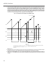
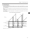
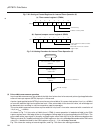
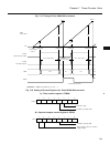
121 chapter 7 timer/counter units 7 (1) basic operation by setting enton (n = 0, 1) of the timer output control register (toc) to 1, the timer outputs (to1, to0) can be changed with the timing determined by mod0, mod1, and clr01 of capture/compare control register 0 (crc0). In addition, by clearing ...
Page 151
122 µ pd78214 sub-series 7.1.7 pwm output the pwm output function outputs a pwm signal whose period coincides with the full-count period of 16-bit timer 0 (tm0). The pulse width of to0 is determined by the value of cr00, and the pulse width of to1 is determined by the value of cr01. Before this func...
Page 152
123 chapter 7 timer/counter units 7 fig. 7-14 example of pwm output using tm0 remark alv0 = 0, alv1 = 0 fig. 7-15 pwm output when cr00 = ffffh remark alv0 = 0 ffffh into00 ffffh ffffh ffffh ffffh to0 tm0 count value count clock period t ovf flag duty factor = × 100 = 99.998(%) 0 1 2 0 1 2 0 pulse wi...
Page 153
124 µ pd78214 sub-series even if the value of a compare register (cr00, cr01) coincides with the value of 16-bit timer 0 (tm0) more than once during one period of pwm output, the output levels on the timer outputs (to0, to1) do not change. Fig. 7-16 example of rewriting compare register cr00 to0 t1 ...
Page 154
125 chapter 7 timer/counter units 7 2. If timer output is disabled (enton = 0: n = 0, 1), the output level on the ton (n = 0, 1) pin is the inverted value of the value set in alvn (n = 0, 1). Accordingly, note that if timer output is disabled when the pwm output function is selected, the active leve...
Page 155
126 µ pd78214 sub-series fig. 7-19 ppg output when cr00 = cr01 fig. 7-20 ppg output when cr00 = 0000h remark alv0 = 0 1 2 n n n intc00 intc01 to0 tm0 count value n-1 0 n-1 2 1 0 0 count period t pulse period = (n + 1)t pulse width = nt t 1 2 n n n intc00 intc01 to0 tm0 count value 0 pulse period = (...
Page 156
127 chapter 7 timer/counter units 7 even if the value of the cr00 compare register coincides with the value of 16-bit timer 0 (tm0) more than once during one period of ppg output, the output levels on the timer outputs (to0, to1) are not inverted. Fig. 7-21 example of rewriting compare register cr00...
Page 157
128 µ pd78214 sub-series 2. If the current value of the cr01 compare register is decreased below the value of 16-bit timer 0 (tm0), the ppg period becomes as long as the full-count time of tm0. At this time, if cr01 is rewritten after the value of the cr00 compare register coincides with the value o...
Page 158
129 chapter 7 timer/counter units 7 7.1.9 sample applications (1) interval timer operation (1) by free running 16-bit timer 0 (tm0), and adding a value to a compare register (cr00, cr01) in an interrupt handling routine, the 16-bit timer/counter can be used as an interval timer whose period is as lo...
Page 159
130 µ pd78214 sub-series fig. 7-25 setting of control registers for interval timer operation (1) (a) timer control register 0 (tmc0) (b) capture/compare control register 0 (crc0) 7 6 5 4 3 2 1 0 0 0 0 0 0 0 0 1 crc0 disables clearing tm0 both to0 and to1 are used for toggle output fig. 7-26 setting ...
Page 160
131 chapter 7 timer/counter units 7 fig. 7-27 interrupt request handling for interval timer operation (1) (2) interval timer operation (2) the 16-bit timer/counter can be used as an interval timer that generates an interrupt at intervals of a count time specified beforehand. (see fig. 7-28.) this in...
Page 161
132 µ pd78214 sub-series fig. 7-29 setting of control registers for interval timer operation (2) (a) timer control register 0 (tmc0) 7 6 5 4 3 2 1 0 0 0 0 0 1 0 0 1 crc0 clears tm0 when cr01 coincides with tm0 both to0 and to1 are used for toggle output (b) capture/compare control register 0 (crc0) ...
Page 162
133 chapter 7 timer/counter units 7 fig. 7-31 timing of pulse width measurement remark d n : tm0 count value (n = 0, 1, 2, ...) fig. 7-32 setting of control registers for pulse width measurement (a) timer control register 0 (tmc0) (b) capture/compare control register 0 (crc0) 7 6 5 4 3 2 1 0 0 0 0 0...
Page 163
134 µ pd78214 sub-series (c) external interrupt mode register 1 (intm1) fig. 7-33 setting procedure for pulse width measurement fig. 7-34 interrupt request handling for pulse width calculation pulse width measurement set crc0 register set intm1 register and mk0l register crc0 ←10h x 0 ←0 ce0 ←1 init...
Page 164
135 chapter 7 timer/counter units 7 (4) pwm output operation in pwm output operation, a pulse signal with a duty factor determined by the value set in a compare register is output. (see fig. 7-35.) the duty factor of a pwm output signal can be changed in steps of 1/65536 from 1/65536 to 65535/65536....
Page 165
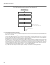
136 µ pd78214 sub-series fig. 7-37 setting procedure for pwm output fig. 7-38 changing duty factor of pwm output cif00 ←0 preprocessing for changing duty factor clear intc00 interrupt request flag ; clears bit 4 of if0l enable intc00 interrupt ; clears bit 4 of mk0l intc00 interrupt duty factor chan...
Page 166
137 chapter 7 timer/counter units 7 (5) ppg output operation in ppg output operation, a pulse signal with a period and duty factor determined by the values set in the compare registers is output. (see fig. 7-39.) fig. 7-40 shows the setting of control registers. Fig. 7-41 shows the setting procedure...
Page 167
138 µ pd78214 sub-series fig. 7-41 setting procedure for ppg output ppg output set crc0 register set toc register set p34 pin in control mode set period in compare register cr01 ; sets bit 3 of tmc0 crc0 ←d8h pmc3.4 ←1 set duty factor in compare register cr00 start counting ce0 ←1 fig. 7-42 changing...
Page 168
139 chapter 7 timer/counter units 7 7.2 8-bit timer/counter 1 7.2.1 functions eight-bit timer/counter 1 can function as an interval timer and can also be used for pulse width measurement. In addition to these basic functions, 8-bit timer/counter 1 can be used as a timer for generating an output trig...
Page 169
140 µ pd78214 sub-series 7.2.2 configuration eight-bit timer/counter 1 consists of one 8-bit timer 1 (tm1), one 8-bit compare register (cr10), and one 8-bit capture/compare register (cr11). Fig. 7-43 shows the block diagram of 8-bit timer/counter 1..
Page 170
141 chapter 7 timer/counter units 7 fig. 7-43 block diagram of 8-bit timer/counter 1 internal bus 8 8 prs12 es01 timer control register 0 (tmc1) clear prs11 prs10 reset 8 8 8 8 8 8 8 ce1 ovf1 8 internal bus overflow reset 8 (crc1) clr11 cm clr10 reset intc10 intc11 real-time output port capture/comp...
Page 171
142 µ pd78214 sub-series (1) 8-bit timer 1 (tm1) tm1 is a timer for counting up with the count clock specified by the lower 4 bits of prescaler mode register 1 (prm1). The count operation of tm1 can be enabled or disabled by timer control register 1 (tmc1). Tm1 allows only read operation using an 8-...
Page 172
143 chapter 7 timer/counter units 7 7.2.3 8-bit timer/counter 1 control registers (1) timer control register 1 (tmc1) the tmc1 register is an 8-bit register for controlling the count operations of 8-bit timer 1 (tm1) and 8-bit timer 2 (tm2). The lower 4 bits control the count operation of tm1 of 8-b...
Page 173
144 µ pd78214 sub-series fig. 7-45 format of prescaler mode register 1 (prm1) 7 6 5 4 3 2 1 0 prm1 prs23 0 prs12 0 0 0 0 0 1 0 1 0 0 1 1 1 0 0 1 0 1 1 1 0 1 1 1 prs10 prs11 specification of count clock [hz] f clk /16 f clk /32 f clk /64 f clk /128 f clk /256 f clk /512 85.3 s 42.7 s 21.3 s 10.7 s 5....
Page 174
145 chapter 7 timer/counter units 7 7.2.4 operation of 8-bit timer 1 (tm1) (1) basic operation eight-bit timer/counter 1 performs count operation by counting up with the count clock specified by the lower 4 bits of prescaler mode register 1 (prm1). When the reset signal is applied, tm1 is cleared to...
Page 175
146 µ pd78214 sub-series (c) when the value of tm1 is ffh count clock tm1 cleared by software ovf1 ovf1 ←0 feh ffh 0h 1h (2) clear operation after a coincidence with a compare register (cr1m: m = 0, 1) or capture operation, 8-bit timer 1 (tm1) can be automatically cleared. If a tm1 clear cause occur...
Page 176
147 chapter 7 timer/counter units 7 fig. 7-49 tm1 cleared after capture operation tm1 count clock n-1 n 0 1 2 intp0 tm1 is captured to cr11 here cleared here tm1 can also be cleared by software when the ce1 bit of the timer control register (tmc1) is reset to 0. Similarly, clear operation is perform...
Page 177
148 µ pd78214 sub-series (b) restart after 0 is set in tm1 cleared count clock tm1 ce1 n-1 n 0 0 1 when the ce1 bit is set to 1 aftr this count clock, counting starts from 0 on the count clock input after the ce1 bit has been set. (c) restart before 0 is set in tm1 cleared count clock tm1 ce1 n-1 wh...
Page 178
149 chapter 7 timer/counter units 7 fig. 7-51 compare operation remark clr10 = 0, clr11 = 0, cm = 0 caution when using an in-circuit emulator, see the notes described in section 7.5.4. Fig. 7-52 tm1 cleared after a coincidence is detected (2) capture operation eight-bit timer/counter 1 performs a ca...
Page 179
150 µ pd78214 sub-series fig. 7-53 capture operation remark d n : tm1 count value (n = 0, 1, 2, ...) clr10 = 0, clr11 = 0, cm = 1 count starts tm1 count value d0 d1 d2 d2 d1 ffh 0h intp0 pin input intp0 interrupt request capture/compare register(cr11) ovf1 d0
Page 180
151 chapter 7 timer/counter units 7 fig. 7-54 tm1 cleared after capture operations remark d n : tm1 count value (n = 0, 1, 2, ...) clr10 = 0, clr11 = 0, cm = 1 7.2.6 sample applications (1) interval timer operation (1) by free running 8-bit timer 1 (tm1), and adding a value to a compare register (cr...
Page 181
152 µ pd78214 sub-series fig. 7-55 timing of interval timer operation (1) n n 0h tm1 count value mod(2n) mod(3n) ffh mod(2n) mod(3n) mod(4n) timer starts compare register (cr10) intc10 interrupt request rewriting by inter- rupt program interval interval interval rewriting by inter- rupt program rewr...
Page 182
153 chapter 7 timer/counter units 7 fig. 7-57 setting procedure for interval timer operation (1) fig. 7-58 interrupt request handling for interval timer operation (1) (2) interval timer operation (2) eight-bit timer/counter 1 can be used as an interval timer that generates an interrupt at intervals ...
Page 183
154 µ pd78214 sub-series fig. 7-59 timing of interval timer operation (2) (when cr11 is used as a compare register) remark interval = (n + 1) × x/f clk , 0 ≤ n ≤ ffh x = 16, 32, 64, 128, 256, 512 fig. 7-60 setting of control registers for interval timer operation (2) (a) timer control register 1 (tm...
Page 184
155 chapter 7 timer/counter units 7 fig. 7-61 setting procedure for interval timer operation (2) (3) pulse width measurement operation in pulse width measurement, the width of the high level or low level of an external pulse signal applied to the external interrupt request (intp0) input pin is measu...
Page 185
156 µ pd78214 sub-series fig. 7-62 timing of pulse width measurement (when cr11 is used as a capture register) remark d n : tm1 count value (n = 0, 1, 2, ...) x = 16, 32, 64, 128, 256, 512 ovf1 capture/compare register (cr11) tm1 count value 0h captured captured (d1 – d0) × x/f clk captured count st...
Page 186
157 chapter 7 timer/counter units 7 fig. 7-63 setting of control registers for pulse width measurement (a) timer control register 1 (tmc1) (b) prescaler mode register 1 (prm1) (c) capture/compare control register 1 (crc1) (d) external interrupt mode register 0 (intm0) 7 6 5 4 3 2 1 0 0 0 1 0 0 crc1 ...
Page 187
158 µ pd78214 sub-series fig. 7-64 setting procedure for pulse width measurement fig. 7-65 interrupt request handling for pulse width calculation set crc1 register set intm0 register and mk0l register crc1 ←04h x 0 ←0 ce1 ←1 initialize buffer memory for capture value start counting ; sets bit 3 of t...
Page 188
159 chapter 7 timer/counter units 7 7.3 8-bit timer/counter 2 7.3.1 functions eight-bit timer/counter 2 has two functions not available with the other three timers/counters: • external event counter • one-shot timer this section describes the following four basic functions in sequence: • interval ti...
Page 189
160 µ pd78214 sub-series (2) programmable square wave output eight-bit timer/counter 2 outputs a square wave separately on the to2 and to3 timer output pins. Table 7-12 programmable square wave output setting range of 8-bit timer/counter 2 maximum pulse width 2 8 × 16/f clk (683 µs) 2 8 × 32/f clk (...
Page 190
161 chapter 7 timer/counter units 7 (4) external event counter eight-bit timer/counter 2 counts clock pulses (ci pin input pulses) applied to the external interrupt input pin (intp2). Table 7-14 indicates the clock signals that can be applied to 8-bit timer/counter 2. Table 7-14 clock signals that c...
Page 191
162 µ pd78214 sub-series fig. 7-66 block diagram of 8-bit timer/counter 2 external interrupt mode register intc21 reset 8 8 8 8 8 8 8 1/8 es21 es20 es11 es10 (intm0) intp1 intp1 intp2/ci intp2 mpx edge detector prs23 prs22 prs21 prs20 edge detector f clk /512 f clk /256 f clk /128 f clk /64 f clk /3...
Page 192
163 chapter 7 timer/counter units 7 (5) output control circuit when the value of cr20 or cr21 coincides with the value of tm2, timer output can be inverted. By setting the higher 4 bits of the timer output control register (toc), a square wave can be output on a timer output pin (to2, to3). At this ...
Page 193
164 µ pd78214 sub-series (2) prescaler mode register 1 (prm1) the prm1 register is an 8-bit register used to specify a count clock for 8-bit timer 1 (tm1) and 8-bit timer 2 (tm2). The higher 4 bits are used to specify a count clock for tm2 of 8-bit timer/counter 2. (the lower 4 bits are used to spec...
Page 194
165 chapter 7 timer/counter units 7 (3) capture/compare control register 2 (crc2) the crc2 register is used to specify the condition for enabling the clear operation of 8-bit timer 2 (tm2) with the cr21 compare register or cr22 capture register, and also specify a timer output (to2, to3) mode. The c...
Page 195
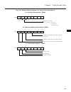
166 µ pd78214 sub-series (4) timer output control register (toc) the toc register is an 8-bit register for controlling the active level of timer output and for enabling/disabling timer output. The higher 4 bits control the timer output operation (on the to2 and to3 pins) of 8-bit timer/counter 2. (t...
Page 196
167 chapter 7 timer/counter units 7 7.3.4 operation of 8-bit timer 2 (tm2) (1) basic operation eight-bit timer/counter 2 performs count operation by counting up with the count clock specified by the higher 4 bits of prescaler mode register 1 (prm1). Bit 7 (ce2) of timer control register 1 (tmc1) is ...
Page 197
168 µ pd78214 sub-series (c) when the value of tm2 is ffh (2) clear operation after a coincidence with the cr21 compare register or capture operation, 8-bit timer 2 (tm2) can be automatically cleared. If a tm2 clear cause occurs, tm2 is cleared to 00h by the next count clock pulse. This means that e...
Page 198
169 chapter 7 timer/counter units 7 tm2 can also be cleared by software when the ce2 bit of the timer control register (tmc1) is reset to 0. Similarly, clear operation is performed by the count clock pulse following the resetting of ce2 bit to 0. If the ce2 bit is set to 1 before tm2 is reset to 0 b...
Page 199
170 µ pd78214 sub-series (c) restart before 0 is set in tm2 cleared count clock tm2 ce2 n-1 when the ce2 bit is set to 1 before this count clock, clearing tm2 by ce2 ←0 and counting by ce2←1 are performed simultaneously. N 0 1 2 7.3.5 external event counter function eight-bit timer/counter 2 can cou...
Page 200
171 chapter 7 timer/counter units 7 fig. 7-75 external event count timing of 8-bit timer/counter 2 (1) when occurrences of one edge are counted (maximum frequency = f clk /24) remark ici: ci input signal after passing through the edge detector (2) when occurrences of both edges are counted (maximum ...
Page 201
172 µ pd78214 sub-series the count operation of tm2 is controlled by the ce2 bit of the tmc1 register as in the case of basic operation. When the ce2 bit is set to 1 by software, tm2 is cleared to 00h by the first count clock pulse, then count-up operation starts. When the ce2 bit is set to 0 by sof...
Page 202
173 chapter 7 timer/counter units 7 fig. 7-77 example where input of no valid edge cannot be distinguished from input of only one valid edge with external event counter cannot be distinguished tm2 1 0 2 ci 0 count starts fig. 7-78 how to distinguish input of no valid edge from input of only one vali...
Page 203
174 µ pd78214 sub-series (b) count value read processing 3. With an in-circuit emulator, digital noise on the ci/intp2 pin cannot be removed correctly. When the event counter function is used, the operation described below is performed if an edge is detected erroneously. • when ie-78210-r is used co...
Page 204
175 chapter 7 timer/counter units 7 7.3.6 one-shot timer function eight-bit timer/counter 2 has an operation mode in which the full-count (ffh) is reached as the result of count operation. Fig. 7-79 one-shot timer operation as shown in fig. 7-79, a one-shot interrupt is generated when the value (00h...
Page 205
176 µ pd78214 sub-series 7.3.7 compare register and capture register operations (1) compare operation eight-bit timer/counter 2 performs an operation to compare the values set in the compare registers with timer count values. When the values set in the compare registers (cr20, cr21) coincide with co...
Page 206
177 chapter 7 timer/counter units 7 fig. 7-81 tm2 cleared after a coincidence is detected remark clr22 = 0 caution when using an in-circuit emulator, see the notes described in section 7.5.4. (2) capture operation eight-bit timer/counter 2 performs a capture operation to load the count value of the ...
Page 207
178 µ pd78214 sub-series fig. 7-82 capture operation remark d n : tm2 count value (n = 0, 1, 2, ...) clr21 = 0, clr22 = 0 d0 d1 d2 d0 d1 d2 (undefined) (undefined) reads cr22 reads cr22 ffh tm2 count value capture register (cr22) intp1 interrupt request intp1 pin input 0h count starts ce ←1 ovf2 cpu...
Page 208
179 chapter 7 timer/counter units 7 fig. 7-83 tm2 cleared after capture operation remark clr21 = 0, clr22 = 1 7.3.8 basic operation of output control circuit the output control circuit controls the levels of the timer outputs (to2, to3) according to the coincidence signal from the compare registers....
Page 209
180 µ pd78214 sub-series table 7-15 timer output (to2, to3) operation toc 0 0 1 1 0 1 1 0 1 1 0 1 1 ento3 0/1 0/1 0/1 0/1 0/1 0/1 0/1 0/1 0/1 0/1 0/1 0/1 0/1 al v3 0 1 0 1 1 0 1 1 0 1 1 0 1 ento2 0/1 0/1 0/1 0/1 0/1 0/1 0/1 0/1 0/1 0/1 0/1 0/1 0/1 al v2 × 0 0 0 0 0 0 1 1 1 1 1 1 mod1 × 0 0 0 1 1 1 0...
Page 210
181 chapter 7 timer/counter units 7 (1) basic operation by setting enton (n = 2, 3) of the timer output control register (toc) to 1, the timer outputs (to2, to3) can be changed with the timing determined by mod0, mod1, and clr21 of capture/compare control register 2 (crc2). In addition, by clearing ...
Page 211
182 µ pd78214 sub-series table 7-16 to2 and to3 toggle output (f clk = 6 mhz) count clock f clk /16 f clk /32 f clk /64 f clk /128 f clk /256 f clk /512 maximum pulse width 2 8 × 16/f clk (683 µs) 2 8 × 32/f clk (1.37 ms) 2 8 × 64/f clk (2.73 ms) 2 8 × 128/f clk (5.46 ms) 2 8 × 256/f clk (10.9 ms) 2...
Page 212
183 chapter 7 timer/counter units 7 table 7-17 pwm output on to2 and to3 (f clk = 6 mhz) count clock f clk /16 f clk /32 f clk /64 f clk /128 f clk /256 f clk /512 minimum pulse width 2.7 5.3 10.7 21.3 42.7 85.3 pwm period (ms) 0.7 1.4 2.7 5.5 10.9 21.8 pwm frequency (hz) 1465 732 366 183 92 46 fig....
Page 213
184 µ pd78214 sub-series fig. 7-87 pwm output when cr20 = ffh remark alv2 = 0 even if the value of a compare register (cr20, cr21) coincides with the value of 8-bit timer 2 (tm2) more than once during one period of pwm output, the output levels on the timer outputs (to2, to3) are not inverted. Fig. ...
Page 214
185 chapter 7 timer/counter units 7 cautions 1. If a value less than the value of 8-bit timer 2 (tm2) is set in a compare register (cr20, cr21), a pwm signal with a 100% duty factor is output. Rewrite the cr20 or cr21 compare register, if required, by using an interrupt generated by a coincidence be...
Page 215
186 µ pd78214 sub-series fig. 7-90 shows an example of ppg output using 8-bit timer 2 (tm2). Fig. 7-91 shows an example of ppg output when cr20 = cr21. Fig. 7-92 shows an example of ppg output when cr20 = 00h. Fig. 7-90 example of ppg output using tm2 remark alv2 = 0, alv3 = 0 table 7-18 ppg output ...
Page 216
187 chapter 7 timer/counter units 7 fig. 7-91 ppg output when cr20 = cr21 remark alv2 = 0 fig. 7-92 ppg output when cr20 = 00h remark alv2 = 0 1 2 n n n intc20 intc21 to2 tm2 count value n-1 0 n-1 2 1 0 0 count period t pulse period = (n + 1)t pulse width = nt t 1 2 n n n intc20 intc21 to2 tm2 count...
Page 217
188 µ pd78214 sub-series even if the value of the cr20 compare register coincides with the value of 8-bit timer 2 (tm2) more than once during one period of ppg output, the output level on the timer output (to2) is not inverted. Fig. 7-93 example of rewriting compare register cr20 to2 t1 t2 t1 t1 t2 ...
Page 218
189 chapter 7 timer/counter units 7 2. If the current value of the cr21 compare register is decreased below the value of 8-bit timer 2 (tm2), the ppg period becomes as long as the full-count time of tm2. At this time, if cr21 is rewritten after the value of the cr20 compare register coincides with t...
Page 219
190 µ pd78214 sub-series 7.3.11 sample applications (1) interval timer operation (1) by free running 8-bit timer 2 (tm2), and adding a value to a compare register (cr20, cr21) in an interrupt handling routine, 8-bit timer/counter 2 can be used as an interval timer whose period is as long as the adde...
Page 220
191 chapter 7 timer/counter units 7 fig. 7-97 setting of control registers for interval timer operation (1) (a) prescaler mode register 1 (prm1) (b) capture /compare control register 0 (crc0) 7 6 5 4 3 2 1 0 0 0 0 0 0 1 crc0 0 0 disables clearing tm2 both to2 and to3 are used for toggle output (c) t...
Page 221
192 µ pd78214 sub-series fig. 7-99 interrupt request handling for interval timer operation (1) (2) interval timer operation (2) eight-bit timer/counter 2 can be used as an interval timer that generates an interrupt at intervals of a count time specified beforehand. (see fig. 7-100.) fig. 7-101 shows...
Page 222
193 chapter 7 timer/counter units 7 fig. 7-101 setting of control registers for interval timer operation (2) (a) prescaler mode register 1 (prm1) (b) capture/compare control register 2 (crc2) (c) timer control register 1 (tmc1) 7 6 5 4 3 2 1 0 prs23 × 0 prm1 specifies count clock (x/f clk ; where x ...
Page 223
194 µ pd78214 sub-series fig. 7-102 setting procedure for interval timer operation (2) (3) pulse width measurement operation in pulse width measurement, the width of the high level or low level of an external pulse signal applied to the intp1 pin is measured. A pulse signal applied to the intp1 pin ...
Page 224
195 chapter 7 timer/counter units 7 fig. 7-103 timing of pulse width measurement remark d n : tm2 count value (n = 0, 1, 2, ...) fig. 7-104 setting of control registers for pulse width measurement (a) prescaler mode register 1 (prm1) (b) capture/compare control register 2 (crc2) 7 crc2 0 0 6 5 4 3 2...
Page 225
196 µ pd78214 sub-series (c) timer control register 1 (tmc1) (d) external interrupt mode register 0 (intm0) fig. 7-105 setting procedure for pulse width measurement set crc1 register set intm0 register and mk0l register crc2 ←10h x 0 ←0 initialize buffer memory for capture value enable interrupt int...
Page 226
197 chapter 7 timer/counter units 7 fig. 7-106 interrupt request handling for pulse width calculation (4) pwm output operation in pwm output operation, a pulse signal with a duty factor determined by the value set in a compare register is output. (see fig. 7-107.) the duty factor of a pwm output sig...
Page 227
198 µ pd78214 sub-series fig. 7-108 setting of control registers for pwm output operation (a) timer control register 1 (tmc1) (b) prescaler mode register 1 (prm1) (c) capture/compare control register 2 (crc2) 7 6 5 4 3 2 1 0 1 crc2 0 0 1 0 0 0 0 disables clearing tm2 both to2 and to3 are used for pw...
Page 228
199 chapter 7 timer/counter units 7 fig. 7-109 setting procedure for pwm output fig. 7-110 changing duty factor of pwm output (5) ppg output operation in ppg output operation, a pulse signal with a period and duty factor determined by the values set in the compare registers is output. (see fig. 7-11...
Page 229
200 µ pd78214 sub-series fig. 7-112 setting of control registers for ppg output operation (a) timer control register 1 (tmc1) (b) prescaler mode register 1 (prm1) (c) capture/compare control register 2 (crc2) 7 6 5 4 3 2 1 0 1 crc2 0 1 1 1 0 0 0 clears when tm2 coincides with cr21 disables clearing ...
Page 230
201 chapter 7 timer/counter units 7 fig. 7-113 setting procedure for ppg output fig. 7-114 changing duty factor of ppg output (6) external event counter operation when functioning as an external event counter, 8-bit timer/counter 2 counts clock pulses externally applied to the ci pin. As shown in fi...
Page 231
202 µ pd78214 sub-series fig. 7-116 setting of control registers for external event counter operation (a) prescaler mode register 1 (prm1) (b) external interrupt mode register 0 (intm0) (c) timer control register 1 (tmc1) fig. 7-117 setting procedure for external event counter operation 7 6 5 4 3 2 ...
Page 232
203 chapter 7 timer/counter units 7 (7) one-shot timer operation when functioning as a one-shot timer, 8-bit timer/counter 2 generates only one interrupt when a specified count time has elapsed after the start of 8-bit timer 2 (tm2). (see fig. 7-118.) an additional one-shot timer operation can be st...
Page 233
204 µ pd78214 sub-series fig. 7-120 setting procedure for one-shot timer operation fig. 7-121 procedure for starting an additional one-shot timer operation one-shot timer set one-shot timer mode ; sets bit 5 of tmc1 to 1 set prm1 register set count value in cr21 register set crc2 register start coun...
Page 234
205 chapter 7 timer/counter units 7 7.4 8-bit timer/counter 3 7.4.1 functions eight-bit timer/counter 3 can be used as an interval timer, and also as a counter for generating a clock signal used with the baud rate generator. When operating as an interval timer, 8-bit timer/counter 3 generates an int...
Page 235
206 µ pd78214 sub-series fig. 7-122 block diagram of 8-bit timer/counter 3 intp4/asck es41,es40 8 8 1/8 es41 es40 intp4 intc30 f clk /512 f clk /256 f clk /128 f clk /64 f clk /32 f clk /16 f clk /8 mpx prs3 prs2 prs1 prs0 8 internal bus 8 timer control register 0 (tmc0) ce3 prescaler mode register ...
Page 236
207 chapter 7 timer/counter units 7 7.4.3 8-bit timer/counter 3 control registers (1) timer control register 0 (tmc0) the tmc0 register is an 8-bit register for controlling the count operation of 8-bit timer 3 (tm3). The higher 4 bits control the count operation of tm3 of 8-bit timer/counter 3. (the...
Page 237
208 µ pd78214 sub-series 7.4.4 operation of 8-bit timer 3 (tm3) (1) basic operation eight-bit timer/counter 3 performs count operation by counting up with the count clock specified by the higher 4 bits of prescaler mode register 0 (prm0). When the reset signal is applied, tm3 is cleared to 00h, and ...
Page 238
209 chapter 7 timer/counter units 7 (2) clear operation after a coincidence with the cr30 compare register, 8-bit timer 3 (tm3) can be automatically cleared. If a tm3 clear cause occurs, tm3 is cleared to 00h by the next count clock pulse. This means that even if a tm3 clear cause occurs, tm3 holds ...
Page 239
210 µ pd78214 sub-series (b) restart after 0 is set in tm3 cleared count clock tm3 ce3 n-1 n 0 0 1 when the ce3 bit is set to 1 after this count clock, counting starts from 0 on the count clock input after the ce3 bit has been set. (c) restart before 0 is set in tm3 cleared count clock tm3 ce3 n-1 w...
Page 240
211 chapter 7 timer/counter units 7 fig. 7-128 compare operation 7.4.6 sample applications (1) interval timer operation eight-bit timer/counter 3 can be used as an interval timer that generates an interrupt at intervals of a count time specified beforehand. Eight-bit timer/counter 3 can also be used...
Page 241
212 µ pd78214 sub-series fig. 7-130 setting of control registers for interval timer operation (a) timer control register 0 (tmc0) (b) prescaler mode register 0 (prm0) 7 6 5 4 3 2 1 0 prs3 0 0 0 0 prm0 prs2 prs1 prs0 specifies count clock (x/f clk ; where x = 16, 32, 64, 128, 256, or 512) fig. 7-131 ...
Page 242
213 chapter 7 timer/counter units 7 (2) the ovfm flag for holding an overflow from a timer/counter is contained in register tmcn used to control the operation of the timer/counter. When a read/modify/write instruction (such as and tmcn,#7fh) is executed, for example, the ovfm flag may be cleared. (e...
Page 243
214 µ pd78214 sub-series fig. 7-132 count start operation (5) even when an instruction is executed to stop a timer (cen ← 0), the value of tmn is not cleared to 0 immediately. Instead, the value of tmn is cleared to 0 by the count clock pulse occurring after an instruction is executed (cen ← 0) to s...
Page 244
215 chapter 7 timer/counter units 7 (6) when a register associated with a timer/counter is accessed, wait states as many as the maximum number of clock pulses note indicated below are automatically inserted. Note one wait state: 1/f clk table 7-20 maximum number of wait states inserted when register...
Page 245
216 µ pd78214 sub-series (9) when pwm is used, a pwm signal with a 100% duty factor is output if a value less than the value of tmn (n = 0, 2) is set in compare register crnm (n = 0, 2, m = 0, 1). Crnm rewrite operation must be performed using an interrupt generated by a coincidence between tmn and ...
Page 246
217 chapter 7 timer/counter units 7 (10)notes on compare register rewrite operation when ppg output is used (a) if a value less than the value of tmn is written into compare register crn0 (n = 0, 2) before the value of the crn0 register coincides with the value of tmn (n = 0, 2), a ppg signal with a...
Page 247
218 µ pd78214 sub-series fig. 7-137 example of ppg output period made longer n3 n1 n2 n4 n2 0h crn0 crn1 top (p = 0,2) n1 n3 n1 n4 n2 n1 full count value n3 n5 tmn the ppg period is extended when a value, n2 less than tmn value, n5 is written to crn1 here. Top becomes inactive when crn0 coincides wi...
Page 248
219 chapter 7 timer/counter units 7 (14) with an in-circuit emulator, digital noise cannot be removed correctly. When a timer/counter is used together with edge detection function, note the point below. (a) when ie-78210-r is used operations are performed on an erroneously detected edge. (b) when ot...
Page 249
220 µ pd78214 sub-series fig. 7-138 interrupt request generation using external event counter countable timing of tm2 tm2 n n-1 n+1 ici ci 8 to 12 clocks 16 clocks (max.) count clock of tm2 coincidence between intp2 and ici tm2 counts up here or is compared with compare register. Ici: signal that ha...
Page 250
221 chapter 7 timer/counter units 7 fig. 7-140 how to distinguish input of no valid edge from input of only one valid edge with external event counter (a) count start processing (b) count value read processing count starts clear intp2 interrupt request flag ; clears pif2 (0) start counting ; sets ce...
Page 251
222 µ pd78214 sub-series (3) with an in-circuit emulator, digital noise cannot be removed correctly. When the timer/counter is used together with edge detection function, note the point below. • when ie-78210-r is used all functions are performed on an erroneously detected edge. • when other in-circ...
Page 252
223 chapter 7 timer/counter units 7 fig. 7-141 interrupt generation timing change by an erroneously detected edge tmn count value (n = 1,2) for pd78214 emulator other than ie-78210-r for pd78214 emulator other than ie-78210-r interrupt generation timing when crnm = n2 (n = 1,2, m = 0,1) interrupt ge...
Page 253
224 µ pd78214 sub-series (c) event counter function (with only 8-bit timer/counter 2) an erroneously detected edge causes no change in the value of the timer/counter. However, the timing for generating an interrupt by a coincidence between the value of the timer/counter and the value of a compare re...
Page 254
225 8 chapter 8 a/d converter the µpd78214 contains an analog-to-digital (a/d) converter with eight multiplexed analog input pins (an0 through an7). This a/d converter uses successive approximation the conversion result is stored in an 8-bit a/d conversion result register (adcr). Conversion can be p...
Page 255
226 µ pd78214 sub-series fig. 8-1 a/d converter configuration successive approximation register (sar) sample and hold circuit series resistor string input selector tap selector r/2 r/2 a/d converter mode register (adm) voltage comparator av ss r av ref selector intad intp5 reset interrupt request 8 ...
Page 256
227 chapter 8 a/d converter 8 cautions 1. To prevent malfunction due to noise, insert a capacitor between each analog input pins (an0 through an7) and the av ss pin and between the reference voltage input pin (av ref ) and the av ss pin. Fig. 8-2 example of capacitors connected to the a/d converter ...
Page 257
228 µ pd78214 sub-series (7) edge detector the edge detector detects the valid edge of an input at the interrupt request input pin (intp5) and generates an external interrupt request signal (intp5) and an external trigger for a/d conversion. The valid edge of an input at the intp5 pin is specified b...
Page 258
229 chapter 8 a/d converter 8 fig. 8-3 a/d converter mode register (adm) format note f clk : system clock frequency 7 6 5 4 3 2 1 0 trg 0 fr cs adm ani2 ani1 ani0 ms fr ani2 ani1 ani0 ms 0 0 0 0 1 1 1 1 0 0 0 0 1 1 1 1 0 0 1 1 0 0 1 1 0 0 1 1 0 0 1 1 0 1 0 1 0 1 0 1 0 1 0 1 0 1 0 1 0 0 0 0 0 0 0 0 1...
Page 259
230 µ pd78214 sub-series 8.3 operation 8.3.1 basic a/d converter operation (1) a/d conversion sequence the a/d converter operates as follows: (a) the input selector selects one of the analog input pins (an0 through an7) according to the mode of operation specified in the a/d converter mode register ...
Page 260
231 chapter 8 a/d converter 8 a/d conversion continues until the cs bit is reset by software. If data is written to the adm register during conversion, conversion is initialized. If the cs bit is 1, conversion is started from the beginning. When the reset signal is input, the adcr register contents ...
Page 261
232 µ pd78214 sub-series (3) a/d conversion time the time required for a/d conversion is determined by the system clock frequency (f clk ) and the fr bit of the adm register. To maintain a/d conversion accuracy above a certain level, it is necessary to set the fr bit as listed in table 8-2 according...
Page 262
233 chapter 8 a/d converter 8 8.3.3 scan mode in the scan mode, signals input from the analog input pins, specified by bits 1 through 3 (ani0 through ani2) of the a/d converter mode register (adm), are selected successively for conversion. For example, when the ani2 through ani0 bits of the adm regi...
Page 263
234 µ pd78214 sub-series 2. If the adm register is set after registers related to interrupts have been set during the scan mode, an unwanted interrupt may occur, thus causing the storage location of the conversion result to appear to have shifted. To prevent this, take the actions listed below in th...
Page 264
235 chapter 8 a/d converter 8 (2) scan-mode a/d conversion when triggered, conversion begins with the signal input to the an0 pin. When the conversion sequence for the an0 pin is completed, the signal at the next analog input pin is converted. Each time a conversion sequence is completed, an interru...
Page 265
236 µ pd78214 sub-series fig. 8-10 example of malfunction in a hardware-started a/d conversion notes 1. When the operation is normal, the result of conversion 2 is stored. If a malfunction occurs, however, value 7fh is stored. 2. Time from when an input to the int5 pin changes to when its edge is as...
Page 266
237 chapter 8 a/d converter 8 fig. 8-11 select-mode a/d conversion started by hardware ann ann ann ann ann anm anm anm ann ann ann intp5 pin input (rising edge valid) a/d conversion standby state adm writing cs ←1, trg←1 adm writing cs ←1, trg←1 adcr intad intad accepted standby state remark n = 0, ...
Page 267
238 µ pd78214 sub-series fig. 8-12 scan-mode a/d conversion started by hardware an0 an2 an1 an0 an0 an1 an2 an1 an0 an1 an0 an0 an0 an2 an1 an0 adcr an0 adm writing cs ← 1, trg ← 1 a/d conversion (scans an0 to an2) standby state intp5 pin input (rising edge valid) intad intad accepted an1 an2 an0 st...
Page 268
239 chapter 8 a/d converter 8 8.4 interrupt request from the a/d converter the a/d converter generates an a/d conversion end interrupt request (intad), each time a conversion sequence is completed, except for the select mode. The interrupt control flags are shared by the intad interrupt and the intp...
Page 269
240 µ pd78214 sub-series (2) about hardware-started a/d conversion (a) eight to twelve system clocks are required from when a valid edge appears at the intp5 pin until a/d conversion is actually started. Take this delay into consideration when designing your application. See chapter 11 for details o...
Page 270
241 chapter 8 a/d converter 8 fig. 8-14 example of malfunction in a hardware-started a/d conversion notes 1. When the operation is normal, the result of conversion 2 is stored. If a malfunction occurs, however, value 7fh is stored. 2. Time from when an input to the int5 pin changes to when its edge ...
Page 271
242.
Page 272
243 9 chapter 9 asynchronous serial interface the µpd78214 contains an asynchronous serial interface, uart (universal asynchronous receiver transmitter). This interface transmits 1-byte data following a start bit and is capable of full-duplex transmission. The µpd78214 also contains a baud rate gene...
Page 273
244 µ pd78214 sub-series fig. 9-1 asynchronous serial interface configuration intst internal bus reception buffer reset txs 1/8 1/8 rxb pe fe ove intsr intser (asis) transmission control parity generation p31/txd p30/rxd 1 16 1 16 selector transmission shift register asynchronous serial interface st...
Page 274
245 chapter 9 asynchronous serial interface 9 (1) reception buffer (rxb) the reception buffer holds the receive data. Each time the shift register receives 1 byte of data, it sends it to this reception buffer. If the data length is specified to be 7 bits, the receive data is sent to bits 0 through 6...
Page 275
246 µ pd78214 sub-series fig. 9-2 format of the asynchronous serial interface mode register (asim) cautions 1. The asynchronous serial interface mode register (asim) must not be modified during transmission. If the asim register is modified during transmission, further transmission becomes impossibl...
Page 276
247 chapter 9 asynchronous serial interface 9 fig. 9-3 format of the asynchronous serial interface status register (asis) caution be sure to read the reception buffer (rxb) contents, even if a reception error occurs. Otherwise, an overrun error will occur when the next data is received, and the erro...
Page 277
248 µ pd78214 sub-series • odd parity in contrast to even parity, the parity bit for odd parity is controlled so that the number of 1 bits in the transmit data becomes odd. When data is received, the number of 1 bits in it is counted, and if the number of 1 bits is even, a parity error is detected. ...
Page 278
249 chapter 9 asynchronous serial interface 9 9.3.4 reception when the rxe bit of the asynchronous serial interface mode register (asim) is set to 1, reception is enabled, and the input to the rxd pin is sampled. Sampling at the rxd pin is performed using the serial clock specified in the asim regis...
Page 279
250 µ pd78214 sub-series table 9-1 causes of reception errors parity error framing error overrun error the parity of the receive data does not match the type of parity specified at transmission. No stop bit is detected note . Before the receive data is read out from the reception buffer, the next da...
Page 280
251 chapter 9 asynchronous serial interface 9 9.4 baud rate generator 9.4.1 configuration of the baud rate generator for uart fig. 9-8 shows the configuration of the baud rate generator. Fig. 9-8 baud rate generator clock configuration (1) 4-bit counter the 4-bit counter counts the internal system c...
Page 281
252 µ pd78214 sub-series fig. 9-9 baud rate generator control register (brgc) format 7 6 5 4 3 2 1 0 brgc ce tps2 tps1 tps0 mdl3 mdl2 mdl1 mdl0 mdl3 mdl2 mdl1 mdl0 k input clock of baud rate generator 0 0 0 0 0 0 0 0 1 1 1 1 1 1 1 1 0 0 0 0 1 1 1 1 0 0 0 0 1 1 1 1 0 0 1 1 0 0 1 1 0 0 1 1 0 0 1 1 0 1...
Page 282
253 chapter 9 asynchronous serial interface 9 9.4.3 operation of the baud rate generator for uart the baud rate generator for uart starts operating, when the ce bit of the baud rate generator control register (brgc) is set to 1. The baud rate clock to be generated is a signal obtained by dividing ei...
Page 283
254 µ pd78214 sub-series 9.5 baud rate setting the baud rate can be set by three methods listed in table 9-2. The table indicates the ranges of baud rates that can be generated by each method, the baud rate calculation formulas, and the selection methods. Table 9-2 baud rate setting j prs3-prs0 0h 1...
Page 284
255 chapter 9 asynchronous serial interface 9 table 9-3 example of setting the brgc register when the baud rate generator for uart is used — fch f9h e9h d9h c9h b9h a9h 99h 89h 92h 84h — 2.44 2.34 2.34 2.34 2.34 2.34 2.34 2.34 2.34 0.00 2.34 oscillation frequency (fxx) or external clock input (fx) 1...
Page 285
256 µ pd78214 sub-series 9.5.2 example of setting the baud rate when 8-bit timer/counter 3 is used table 9-4 lists examples of setting the baud rate when 8-bit timer/counter 3 is used. When using 8-bit timer/ counter 3, reset the sck bit of the asynchronous serial interface mode register (asim) to 0...
Page 286
257 chapter 9 asynchronous serial interface 9 table 9-4 example of setting the baud rate when 8-bit timer/counter 3 is used (asynchronous serial interface) f clk /16 f clk /8 f clk /8 f clk /8 f clk /8 f clk /8 f clk /8 f clk /8 — — 0.16 0.03 0.16 0.16 0.16 2.34 2.34 2.34 — — oscillation frequency f...
Page 287
258 µ pd78214 sub-series 9.5.3 example of setting the brgc when the external baud rate input (asck) is used table 9-5 lists examples of setting the brgc register when an external baud rate input (asck) is used. To use the asck input, set the sck bit of the asynchronous serial interface mode register...
Page 288
259 10 chapter 10 clock synchronous serial interface 10.1 function the clock synchronous serial interface of the µpd78214 is configured as shown in fig. 10-1. The clock synchronous serial interface supports the following two operation modes: (1) three-wire serial i/o mode (msb first) three lines, se...
Page 289
260 µ pd78214 sub-series fig. 10-1 block diagram of the clock synchronous serial interface internal bus d cls1 cls0 f clk /32 f clk /8 8-bit timer/counter 3 output 1/2 serial clock selector intcsi interrupt signal generator circuit bus release/command/ acknowledge detector circuit serial clock count...
Page 290
261 chapter 10 clock synchronous serial interface 10 (1) shift register (sio) converts 8-bit serial data into 8-bit parallel data and vice versa. The sio is used for both transmission and reception. Data is shifted in (received) or shifted out (transmitted) from the msb. The actual transmission/rece...
Page 291
262 µ pd78214 sub-series 10.3 control registers 10.3.1 clock synchronous serial interface mode register (csim) this 8-bit register specifies a serial interface operation mode, serial clock and wake-up function. The 8-bit manipulation instruction and bit manipulation instruction can read and write th...
Page 292
263 chapter 10 clock synchronous serial interface 10 10.3.2 serial bus interface control register (sbic) the sbic register consists of bits that control the status of the serial bus, as well as bits that indicate the status of the data input from the serial bus. This 8-bit register can be used only ...
Page 293
264 µ pd78214 sub-series fig. 10-3 format of serial bus interface control register (sbic) ★ sbic bsye ackd acke ackt cmdd reld cmdt relt 7 6 5 4 3 2 1 0 relt trigger output control for bus release signal (rel) 0 not output 1 output cmdt trigger output control for command signal (cmd) 0 not output 1 ...
Page 294
265 chapter 10 clock synchronous serial interface 10 10.4 operations in the three-wire serial i/o mode in three-wire serial i/o mode, the device can communicate with a device having a conventional clock synchronous serial interface. Basically, communication is performed over three lines of serial cl...
Page 295
266 µ pd78214 sub-series fig. 10-5 timing in three-wire serial i/o mode notes master cpu : output slave cpu : input in three-wire serial i/o mode, the so pin sends a cmos push-pull output. Remark when connecting the device to a device having two-wire serial i/o, connect a buffer to the so pin as sho...
Page 296
267 chapter 10 clock synchronous serial interface 10 10.4.2 operation when only transmission is permitted transmission is enabled when the ctxe bit of the clock synchronous serial interface mode register (csim) is set (1). If the ctxe bit is set, writing the contents of the shift register (sio) invo...
Page 297
268 µ pd78214 sub-series (1) selecting the internal clock as the serial clock when transmission and reception are started, the serial clock is output from the sck pin. In synchronization with the falling edge of the serial clock, data is sequentially output from the sio to the so pin. In synchroniza...
Page 298
269 chapter 10 clock synchronous serial interface 10 (2) function to select a chip by its address the master sends an address to select a slave chip. (3) wake-up function using the wake-up function (which can be set or released by software), a slave device can easily detect whether it receives the a...
Page 299
270 µ pd78214 sub-series 10.5.2 configuration of the serial interface fig. 10-9 is a block diagram of the µpd78214. The serial clock pin (sck) and serial data bus pin sb0 are configured as shown in fig. 10-8. (1) sck: pin to input/output the serial clock • master : cmos push-pull output • slave : sc...
Page 300
271 chapter 10 clock synchronous serial interface 10 fig. 10-9 block diagram of clock synchronous serial interface internal bus d cls1 cls0 f clk /32 f clk /8 intcsi interrupt signal generator circuit bus release/command/ acknowledge detector circuit serial clock counter serial clock control circuit...
Page 301
272 µ pd78214 sub-series 10.5.3 detecting an address match sbi communication is started when a slave device is selected according to the address sent by the master device. The software detects whether the address of a slave device matches the sent address. In the wake-up state (wup set to 1), the sl...
Page 302
273 chapter 10 clock synchronous serial interface 10 fig. 10-10 format of clock synchronous serial interface mode register (csim) caution do not change ctxe from 0 to 1 or crxe from 1 to 0, or vice versa, by means of a single instruction. If this is attempted, the serial clock counter will malfuncti...
Page 303
274 µ pd78214 sub-series (2) serial bus interface control register (sbic) this 8-bit register consists of bits controlling the serial bus statuses and flags indicating the statuses of data input from the serial bus. The 8-bit manipulation instruction and bit manipulation instruction can read and wri...
Page 304
275 chapter 10 clock synchronous serial interface 10 fig. 10-11 format of sbic register (2/2) remarks (r) : read-only (w) : write-only (r/w): read/write ★ acknowledge trigger bit (w) acknowledge enable bit (r/w) acknowledge detection flag (r) busy enable bit (r/w) 1 ackt do not set this bit to 1 bef...
Page 305
276 µ pd78214 sub-series (3) shift register (sio) this 8-bit shift register is used for parallel-serial conversion. The data written into the sio is output to the serial data bus. The data on the serial data bus is read into the sio. Fig. 10-12 shows the configuration of the shift register and relat...
Page 306
277 chapter 10 clock synchronous serial interface 10 10.6 sbi communication and signals this section describes the format of the sbi serial data and signals to be used. Serial data transferred via sbi can be divided into three groups: address, command, and data. Each frame of serial data is formed a...
Page 307
278 µ pd78214 sub-series 10.6.2 command signal (cmd) the command signal is the sb0 line going from high to low while the sck line is high (the serial clock is not output). The master device outputs this signal. Fig. 10-15 command signal sck sb0 "h" the slave device contains the hardware to detect th...
Page 308
279 chapter 10 clock synchronous serial interface 10 10.6.4 command and data the master device sends commands to, and sends or receives data to or from, the slave device selected according to the specified address. Fig. 10-18 command sck sb0 1 2 3 4 5 6 7 8 command c7 c6 c5 c4 c3 c2 c1 c0 command si...
Page 309
280 µ pd78214 sub-series 10.6.6 busy signal (busy) and ready signal (ready) the busy signal informs the master device that the slave device is preparing for data transmission or reception. The ready signal informs the master device that the slave device is ready for data transmission or reception. F...
Page 310
281 chapter 10 clock synchronous serial interface 10 fig. 10-23 ackt operation caution do not set ackt before transfer has been completed. Fig. 10-24 acke operations (a) when acke is set to 1 at the end of transfer (b) when acke is set after transfer has been completed (c) when acke is set to 0 at t...
Page 311
282 µ pd78214 sub-series (d) when acke is set to 1 for a short period of time fig. 10-25 ackd operations (a) when the ack signal is output during the ninth cycle of the sck clock sck sb0 acke the ack signal is not output when acke is set or cleared during this period, and acke = 0 at the falling edg...
Page 312
283 chapter 10 clock synchronous serial interface 10 fig. 10-26 bsye operation sck sb0 bsye 9 busy 8 7 6 ack when bsye = 1 at this point when reset operation is executed during this period and bsye = 0 at the falling edge of sck. D2 d1 d0
Page 313
284 µ pd78214 sub-series table 10-2 signals in sbi mode (1/3) sck sb0 “ h ” “ h ” sck sb0 rising edge of sb0 while sck is set to 1 falling edge of sb0 while sck is set to 1 bus release signal (rel) command signal (cmd) output device definition • relt is set. • cmdt is set. Output condition • reld is...
Page 314
285 chapter 10 clock synchronous serial interface 10 table 10-2 signals in sbi mode (2/3) low signal output to sb0 within a single cycle of the sck clock after serial reception has been completed low sgnal output to sb0, following the acknowledge signal high signal output to sb0 before serial transf...
Page 315
286 µ pd78214 sub-series table 10-2 signals in sbi mode (3/3) notes 1. If wup is set to 0, csiif is always set at the rising edge of the eighth pulse of the sck clock. If wup is set to 1, csiif is set at the rising edge of the eighth pulse of the sck clock only when an address is received. 2. Data i...
Page 316
287 chapter 10 clock synchronous serial interface 10 10.6.8 communication in sbi communication, the master device outputs an address on the serial bus and, usually, one target slave device is selected out of two or more devices according to the address. Once the target device has been determined, co...
Page 317
288 µ pd78214 sub-series fig. 10-27 sending an address from master device to slave device program processing hardware operation program processing sck pin 12 345 6 78 sb0 pin a7 hardware operation a6 a5 a4 a3 a2 a1 a0 ack ready address master device processing (transmitter) transfer line slave devic...
Page 318
289 chapter 10 clock synchronous serial interface 10 fig. 10-28 sending a command from master device to slave device program processing hardware operation program processing sck pin 12 345 6 78 sb0 pin c7 hardware operation c6 c5 c4 c3 c2 c1 c0 ack ready command master device processing (transmitter...
Page 319
290 µ pd78214 sub-series fig. 10-29 sending data from master device to slave device program processing hardware operation program processing sck pin 12 345 6 78 sb0 pin d7 hardware operation d6 d5 d4 d3 d2 d1 d0 ack ready data master device processing (transmitter) transfer line slave device process...
Page 320
291 chapter 10 clock synchronous serial interface 10 fig. 10-30 sending data from the slave device to the master device program processing hardware operation program processing sck pin 12 345 6 78 12 sb0 pin busy ready d7 hardware operation d6 d5 d4 d3 d2 d1 d0 ack busy d7 d6 ready data master devic...
Page 321
292 µ pd78214 sub-series 10.7 notes (1) do not change ctxe from 0 to 1 and crxe from 1 to 0, or vice versa, by means of a single instruction. If this is attempted, the serial clock counter will malfunction and the first communication after the change will be terminated before the eighth bit is sent....
Page 322
293 11 chapter 11 edge detection function pins p20 to p26 support an edge detection function to program a rising or falling edge. The detected edge is sent to the internal hardware. Table 11-1 shows the relationship between pins p20 to p26, and the use of the detected edge. Table 11-1 pins p20 to p2...
Page 323
294 µ pd78214 sub-series fig. 11-1 format of external interrupt mode register 0 (intm0) es21 7 es20 6 es11 5 es10 4 es01 3 es00 2 0 1 esnmi 0 intm0 es01 falling edge specifies edge to be detected on p21 (intp0, cr11 capture trigger, real-time output port output trigger) 0 es00 0 esnmi falling edge s...
Page 324
295 chapter 11 edge detection function 11 fig. 11-2 format of external interrupt mode register 1 (intm1) 0 7 0 6 es51 5 es50 4 es41 3 es40 2 es31 1 es30 0 intm1 es31 falling edge specifies edge to be detected on p24 (intp3, cr02 capture trigger) 0 es30 0 rising edge 0 1 inhibited 1 0 both falling an...
Page 325
296 µ pd78214 sub-series 11.2 edge detection on pin p20 an edge on pin p20 is detected after noise elimination by means of analog delay. A pulse width of at least 10 µs is required to detect the edge. Fig. 11-3 edge detection on pin p20 caution because noise elimination by analog delay is performed ...
Page 326
297 chapter 11 edge detection function 11 11.3 edge detection on pins p21 to p26 an edge on pins p21 to p26 is detected after digital noise elimination by means of clock sampling. The digital noise elimination is performed by means of sampling with the f clk /4 clock. The input signal is eliminated ...
Page 327
298 µ pd78214 sub-series (b) erroneously detected edge during input of a high signal intpn input (n = 0 to 6) erroneously detected edge f clk /4 after noise rejection falling edge detection rising edge detection noise "l" if the ie-78210-r is used, the real-time output port, timer/counter, and a/d c...
Page 328
299 chapter 11 edge detection function 11 (5) if noise input to pins p21 to p26 is synchronized with the f clk /4 clock of the µpd78214, it may not be judged as being noise. If the input of such noise is possible, add a filter to the input pin so that the noise can be eliminated. (6) an in-circuit e...
Page 329
300 µ pd78214 sub-series • compare operation of the timer/counter : if the mode for carrying out a clear operation after a capture operation is selected, or if timer/counter 2 is used as an external event counter, the erroneously detected edge causes the timing of match interrupt generation to be ch...
Page 330
301 12 chapter 12 interrupt functions the µpd78214 has the following two interrupt handling modes. Either mode can be selected by the program. Interrupt handling by a macro service is limited to the interrupt request sources provided with a macro service handling mode listed in table 12-1. Table 12-...
Page 331
302 µ pd78214 sub-series 12.1 interrupt request sources the µpd78214 has 19 interrupt request sources shown in table 12-2. Each of these sources is assigned an interrupt vector table. Table 12-2 interrupt request sources software nonmaskable maskable interrupt request type none none 0 1 2 3 4 5 6 7 ...
Page 332
303 chapter 12 interrupt functions 12 12.1.2 nonmaskable interrupt request a nonmaskable interrupt request is input to the nmi pin. When a valid edge, specified by bit 0 (esnmi) of external interrupt mode register 0 (intm0), is input to the nmi pin, an interrupt request is generated. A nonmaskable i...
Page 333
304 µ pd78214 sub-series (2) selecting intp5 or intad interrupt intp5 or intad is selected by the a/d converter mode register (adm). (either of these interrupts is selected automatically, according to the mode of operation specified for the a/d converter.) both 8-bit manipulation instruction and bit...
Page 334
305 chapter 12 interrupt functions 12 table 12-3 flags for interrupt request sources intp0 intp1 intp2 intp3 intc00 intc01 intc10 intc11 intc21 intp4 intc30 intp5 intad intc20 intser intsr intst intcsi interrupt request source interrupt request flag pif0 pif1 pif2 pif3 cif00 cif01 cif10 cif11 cif21 ...
Page 335
306 µ pd78214 sub-series 12.2.2 interrupt mask register (mk0) the mk0 register is a 16-bit register consisting of interrupt mask flags. Each interrupt mask flag enables or disables the corresponding interrupt request. When the reset signal is input, the register is set to ffffh, thus disabling all m...
Page 336
307 chapter 12 interrupt functions 12 when a low-priority vectored interrupt is being handled, vectored interrupt requests with lower and higher priorities are accepted for multiple-interrupt handling provided that interrupts are enabled. When a high-priority interrupt is being handled, high-priorit...
Page 337
308 µ pd78214 sub-series 12.2.6 program status word (psw) the psw is a register that holds the result of instruction execution and the current status of interrupt requests. The register is mapped with the ie flag that specifies whether to enable maskable interrupts and the isp flag to control multip...
Page 338
309 chapter 12 interrupt functions 12 resetting the nmis bit to 0 during execution of a nonmaskable interrupt service program enables multiple- interrupt handling for nonmaskable interrupt requests. If the nmis bit is 0, a new nonmaskable interrupt request is accepted even when a nonmaskable interru...
Page 339
310 µ pd78214 sub-series (c) if a new nmi request occurs during execution of an nmi service program (when the nmis bit is reset to 0 by the current nmi service program after the nmi request occurs) (d) if two new nmi requests occur during execution of an nmi service program (when the nmis bit is not...
Page 340
311 chapter 12 interrupt functions 12 3. Nonmaskable interrupts are always accepted except during execution of the nonmaskable interrupt handling program (except when multiple-interrupt handling for nonmaskable interrupts have been enabled by resetting the nmis bit of the ist register to 0 during ex...
Page 341
312 µ pd78214 sub-series fig. 12-10 interrupt handling algorithm interrupts for ××pr = 0 occur simultaneously? ××if = 1? ××mk = 0? ××pr = 0? Yes (interrupt request occurs) yes no (low priority) no no ××ism = 0? Yes ie = 1? Yes (ei) isp = 1? Yes vectored interrupt processing higher-priority interrupt...
Page 342
313 chapter 12 interrupt functions 12 12.3.4 multiple-interrupt handling the µpd78214 performs multiple-interrupt handling in which another interrupt request is accepted during one interrupt is already being handled. Multiple-interrupt handling runs according to priority. Priority control is based o...
Page 343
314 µ pd78214 sub-series fig. 12-11 example of handling an interrupt request when an interrupt is already being handled (1/2) main routine processing a vectored interrupt request e (high priority) → vectored interrupt request a (low priority) → processing b processing c processing d → macro service ...
Page 344
315 chapter 12 interrupt functions 12 fig. 12-11 example of handling an interrupt request when an interrupt is already being handled (2/2) main routine processing i vectored interrupt request k (low priority) → vectored interrupt request i (low priority) → [nesting 1] [nesting 2] processing j proces...
Page 345
316 µ pd78214 sub-series fig. 12-12 example of handling interrupts that occur simultaneously 12.3.5 interrupt request and macro service pending when any of the following instructions is executed, all interrupts (including nonmaskable interrupts) and macro services are kept pending. The pending state...
Page 346
317 chapter 12 interrupt functions 12 example of correct coding (2) loop: bt if0h.3, $next br $loop next: ← 2. In addition, when you have to use a coding of the instructions listed above consecutively, yet expect frequent occurrence of interrupts and macro services, insert nop instructions in the co...
Page 347
318 µ pd78214 sub-series 3. “peripheral ram” corresponds to the internal ram at addresses 0fc80h through 0fdffh (for the µpd78212, 0fd80h through 0fdffh). 4. 1 clock = 1/f clk (167 ns at 12 mhz). (3) macro service processing time the time required to process a macro service varies, depending on the ...
Page 348
319 chapter 12 interrupt functions 12 12.4 macro service function 12.4.1 macro service outline macro service is one of the interrupt handling methods. When a vectored interrupt is processed, the contents of the program counter (pc) and the program status word (psw) are saved in the stack and the pc ...
Page 349
320 µ pd78214 sub-series 12.4.2 macro service types the macro service can be used by the 17 types of interrupts listed in table 12-7 (of which, 15 types can use macro services simultaneously). In addition, three modes of operation are available, and each should be selected according to the applicati...
Page 350
321 chapter 12 interrupt functions 12 (3) type c transfers 1-byte data from memory to the real-time output port and the compare register for 8-bit timer/ counter 1 upon each interrupt request. When a specified number of data transfers are performed, a vectored interrupt request is generated. Type c ...
Page 351
322 µ pd78214 sub-series 12.4.4 macro service control register (1) macro service control word the macro service function of the µpd78214 is controlled using the macro service mode registers and macro service channel pointers. The macro service mode registers specify the mode of macro service process...
Page 352
323 chapter 12 interrupt functions 12 (2) macro service mode register a macro service mode register is an 8-bit register that specifies the mode of macro service operation. It is mapped in internal ram as part of macro service control word (see fig 12-16). Fig. 12-17 shows the format of the macro se...
Page 353
324 µ pd78214 sub-series table 12-8 interrupt requests that can specify macro service and related sfrs (type a) interrupt request specifying the type a macro service transfer source/destination sfr cr10 register cr11 register cr20 register cr21 register cr30 register rxb register txs register sio re...
Page 354
325 chapter 12 interrupt functions 12 fig. 12-18 flow of data transfer by macro service (type a) accepts macro service request read contents of macro service mode register identify channel type read channel pointer contents (m) read msc contents (n) buffer address calculation m – n identify transfer...
Page 355
326 µ pd78214 sub-series (2) macro service channel configuration a channel pointer and a macro service counter (msc) specify the addresses of transfer source and destination buffers in the internal ram (at fe00h through feffh). (see fig. 12-19.) the sfr to be accessed is predetermined for each inter...
Page 356
327 chapter 12 interrupt functions 12 (3) example of using the type a macro service the following example shows how data received through an asynchronous serial interface is transferred to a buffer area in the internal ram. Fig. 12-20 asynchronous serial reception 12.4.6 type b macro service (1) ope...
Page 357
328 µ pd78214 sub-series fig. 12-21 flow of data transfer by macro service (type b) accepts macro service request read contents of macro service mode register identify channel type read channel pointer contents (m) identify transfer direction read data from sfr and write it to the memory addressed b...
Page 358
329 chapter 12 interrupt functions 12 (2) macro service channel configuration the macro service pointer (mp) indicates a data buffer area in the 64k memory space as a transfer source or destination. The sfr pointer (sfrp) is set with the lower 8 bits of the address of an sfr used as a transfer sourc...
Page 359
330 µ pd78214 sub-series (3) example of using the type b macro service the following example shows how parallel data is input from port 3 in synchronization with an external signal. The external signal is input to the external interrupt pin (intp4). Fig. 12-23 parallel data input in synchronization ...
Page 360
331 chapter 12 interrupt functions 12 12.4.7 macro service type c (1) operation the type c macro service controls 8-bit timer/counter 1 and the real-time output port simultaneously. This macro service transfers data to both the compare register for 8-bit timer/counter 1 and the buffer register for t...
Page 361
332 µ pd78214 sub-series fig. 12-25 flow of data transfer by macro service (type c) accepts macro service request read contents of macro service mode register identify channel type read channel pointer contents (m) read memory addressed by mpt automatic addition? Increment mptl yes no yes type c oth...
Page 362
333 chapter 12 interrupt functions 12 ring control? Decrement ring counter ring counter = 0? Vectored interrupt request occurs no no yes no subtract modulo register contents from low-order 8-bits of macro service pointer for data (mpdl) and return pointer to the first address msc = 0? 1 yes reload m...
Page 363
334 µ pd78214 sub-series (2) macro service channel configuration there are two types of type c macro service channels, as shown in fig. 12-26. The timer macro service pointer (mpt) indicates a data buffer area in the 64k memory space from which data is transferred to, or added to the contents of, th...
Page 364
335 chapter 12 interrupt functions 12 (b) with ring control modulo register (mr) ring counter (rc) macro service counter (msc) data macro service pointer, low (mpdl) data macro service pointer, high (mpdh) timer macro service pointer, low (mptl) timer macro service pointer, high (mpth) mode register...
Page 365
336 µ pd78214 sub-series (3) example of using the type c macro service the following example shows a pattern output to the real-time output port and how the output interval is controlled directly. Update data is transferred from two data areas previously set in the 64k-byte space to the buffer regis...
Page 366
337 chapter 12 interrupt functions 12 fig. 12-28 data transfer control timing (4) example of using automatic addition control and ring control (a) automatic addition control the automatic addition control function adds the output timing data ( ∆t) specified by a macro service pointer (mpt) to the co...
Page 367
338 µ pd78214 sub-series fig. 12-29 four-phase stepping motor with phase 1 excitation fig. 12-30 four-phase stepping motor with phases 1 and 2 excitation 1 2 3 4 1 2 3 1 cycle (4 patterns) phase a phase b phase c phase d 1 8 2 3 4 5 6 7 8 1 2 3 4 5 1 cycle (8 patterns) phase a phase b phase c phase ...
Page 368
339 chapter 12 interrupt functions 12 fig. 12-31 block diagram 1 for automatic addition control plus ring control (constant-speed rotation with phases 1 and 2 excitation) msc ff –1 ring counter (rc) 08 –1 modulo register (mr) 08 mpdl 00 +1 mpdh b0 mptl 00 mpth b1 mode register ce channel pointer cf ...
Page 369
340 µ pd78214 sub-series fig. 12-32 timing chart 1 for automatic addition control plus ring control (constant-speed rotation with phases 1 and 2 excitation) t0 t2 t1+ ∆t t3 t2+ ∆t t4 t3+ ∆t t5 t4+ ∆t t6 t5+ ∆t t7 t6+ ∆t t8 t7+ ∆t t9 t8+ ∆t t10 t9+ ∆t d0 d2 d3 d4 d5 d6 d7 d0 d1 d2 d3 ∆t ffh count sta...
Page 370
341 chapter 12 interrupt functions 12 fig. 12-33 block diagram 2 for automatic addition control plus ring control (with the output timing varied by phase 2 excitation) msc ff –1 ring counter (rc) 04 –1 modulo register (mr) 04 mpdl 00 +1 mpdh b0 mptl 00 mpth b1 mode register ee channel pointer cf mac...
Page 371
342 µ pd78214 sub-series fig. 12-34 timing chart 2 for automatic addition control plus ring control (with the output timing varied by phase 2 excitation) ∆t9 t1 t0+ ∆t1 t2 t1+ ∆t2 t3 t2+ ∆t3 t4 t3+ ∆t4 t5 t4+ ∆t5 t6 t5+ ∆t6 t7 t6+ ∆t7 t8 t7+ ∆t8 t9 t8+ ∆t9 t0 d2 d3 d0 d1 d2 d3 d0 d1 d2 d1 ∆t8 ∆t6 ∆t...
Page 372
343 chapter 12 interrupt functions 12 12.5 notes (1) do not use the reti instruction to return from the software interrupt. (2) a macro service request is accepted and processed even when a nonmaskable interrupt service program is running. To disable macro service processing during execution of the ...
Page 373
344 µ pd78214 sub-series example of correct coding (2) loop: bt if0h.3, $next br $loop next: ← (6) in addition, when you have to use a coding of the instructions listed in section 12.3.5 consecutively, yet expect frequent occurrence of interrupts and macro services, insert nop instructions in the co...
Page 374
345 13 chapter 13 local bus interface function the local bus interface function is provided to connect external memories (rom and ram) and i/os. External memories (rom and ram) and i/os are accessed by using the rd, wr, and astb signals, a multiplexed address/data bus consisting of lines ad0 to ad7,...
Page 375
346 µ pd78214 sub-series 13.1 control registers 13.1.1 memory expansion mode register (mm) the mm register is an 8-bit register for controlling externally expanded memory, specifying the number of wait states (address space: 00000h to 0ffffh), and controlling the internal fetch cycle. The mm registe...
Page 376
347 chapter 13 local bus interface function 13 13.1.2 programmable wait control register (pw) the pw register is an 8-bit register for specifying the number of wait states for external expansion data memory space 10000h to fffffh. The pw register can be read and written with both 8-bit manipulation ...
Page 377
348 µ pd78214 sub-series fig. 13-3 read timing higher address lower address (output) data (input) hi-z hi-z a8-a15 (output) ad0-ad7 astb (output) rd (output) hi-z fig. 13-4 write timing higher address lower address data hi-z hi-z a8-a15 ad0-ad7 (output) astb (output) wr (output) hi-z caution externa...
Page 378
349 chapter 13 local bus interface function 13 fig. 13-5 accessing expansion data memory (a) read cycle rd (output) a16-a19 (output) contents of p6/pm6 register higher address higher address lower address (output) hi-z hi-z program (input) lower address (output) data (input) hi-z hi-z hi-z a8-a15 (o...
Page 379
350 µ pd78214 sub-series 13.2.3 memory mapping with expanded memory figs. 13-6 to 13-9 show the memory maps when the memory has been expanded. Even when the memory has been expanded, external devices at the same addresses as those of the internal rom area, internal ram area, or sfr area (excluding t...
Page 380
351 chapter 13 local bus interface function 13 fig. 13-6 data memory expansion for µpd78212 (when ea = l) internal ram external sfr area sfr 0fd7fh 0fd80h 0feffh 0ff00h 0ffd0h 0ffffh 0ffdfh 00000h mm6 = 0 external memory internal ram external sfr area sfr 10000h mm6 = 1 external memory expansion dat...
Page 381
352 µ pd78214 sub-series fig. 13-7 data memory expansion for µpd78212 (when ea = h) internal ram external sfr area sfr external memory internal ram external sfr area sfr 10000h mm2, mm1, mm0 = 1, 1, 1 mm6 = 1 external memory expansion data memory fffffh internal rom internal rom mm2, mm1, mm0 = 1, 1...
Page 382
353 chapter 13 local bus interface function 13 fig. 13-8 data memory expansion for µpd78213 and µpd78214 (when ea = l) internal ram external sfr area sfr 0fcffh 0fd00h 0feffh 0ff00h 0ffd0h 0ffffh 0ffdfh 00000h mm6 = 0 external memory internal ram external sfr area sfr 10000h mm6 = 1 external memory ...
Page 383
354 µ pd78214 sub-series fig. 13-9 data memory expansion for µpd78214 and µpd78p214 (when ea = h) internal ram external sfr area sfr external memory internal ram external sfr area sfr 10000h mm2, mm1, mm0 = 1, 1, 1 mm6 = 1 external memory expansion data memory fffffh internal rom internal rom mm2, m...
Page 384
355 chapter 13 local bus interface function 13 13.2.4 example of connecting memories fig. 13-10 shows an example of connecting memories to the µpd78214. In this example, a prom, sram, and mask-programmable rom are connected to the µpd78214. Addresses are assigned to these memories as follows: • prom...
Page 385
356 µ pd78214 sub-series fig. 13-10 example of connecting memories to µpd78214 pd23c4000a µ pd43256ac-12 µ pd27c512d-15 µ le d0-d7 oe q0-q7 ad0-ad7 astb a8-a14 oe ce a17 a16 a15 a14 a-1-a13 cs we oe a19 a18 a17 a16 q4 q3 q2 q1 d4 d3 d2 d1 st st g2a c b a g2b word/byte 74hc04 74hc32 o0-o7 i/o1-i/o8 a...
Page 386
357 chapter 13 local bus interface function 13 13.3 internal rom high-speed fetch function the µpd78212, µpd78214, and µpd78p214 contain an internal rom. The internal rom can be accessed quickly without having to use the bus control circuit. Usually, internal rom is fetched at the same speed as exte...
Page 387
358 µ pd78214 sub-series fig. 13-11 wait control space of µpd78212 (when ea = l) internal ram external sfr area sfr 0fd7fh expansion data memory 00000h external memory 0fd80h 0feffh 0ff00h 0ffffh 10000h 0ffdfh 0ffd0h fffffh space subject to wait control by pw register space subject to wait control b...
Page 388
359 chapter 13 local bus interface function 13 fig. 13-12 wait control space of µpd78212 (when ea = h) internal ram external sfr area sfr 0fd7fh expansion data memory 00000h external memory 0fd80h 0feffh 0ff00h 0ffffh 10000h 0ffdfh 0ffd0h space subject to wait control by pw register space subject to...
Page 389
360 µ pd78214 sub-series fig. 13-13 wait control space of µpd78213 and µpd78214 (when ea = l) internal ram external sfr area sfr 0fcffh expansion data memory 00000h external memory 0fd00h 0feffh 0ff00h 0ffffh 10000h 0ffdfh 0ffd0h fffffh space subject to wait control by pw register space subject to w...
Page 390
361 chapter 13 local bus interface function 13 fig. 13-14 wait control space of µpd78214 and µpd78p214 internal ram external sfr area sfr 0fcffh expansion data memory 00000h external memory 0fd00h 0feffh 0ff00h 0ffffh 10000h 0ffdfh 0ffd0h space subject to wait control by pw register space subject to...
Page 391
362 µ pd78214 sub-series fig. 13-15 read timing of programmable wait function (1/2) (a) when zero wait states are set higher address lower address (output) data (input) hi-z hi-z a8-a15 (output) ad0-ad7 astb (output) rd (output) hi-z f clk note (b) when one wait state is set higher address lower add...
Page 392
363 chapter 13 local bus interface function 13 fig. 13-15 read timing of programmable wait function (2/2) (c) when two wait states are set higher address lower address (output) data (input) hi-z hi-z a8-a15 (output) ad0-ad7 astb (output) rd (output) f clk note note f clk : system clock frequency (f ...
Page 393
364 µ pd78214 sub-series fig. 13-16 write timing of programmable wait function (1/2) (a) when zero wait states are set higher address lower address data hi-z hi-z a8-a15 (output) ad0-ad7 (output) astb (output) wr (output) hi-z f clk note (b) when one wait state is set higher address lower address da...
Page 394
365 chapter 13 local bus interface function 13 fig. 13-16 write timing of programmable wait function (2/2) (c) when two wait states are set higher address lower address data hi-z hi-z a8-a15 (output) ad0-ad7 (output) astb (output) wr (output) hi-z f clk note note f clk : system clock frequency (f xx...
Page 395
366 µ pd78214 sub-series fig. 13-17 timing when external wait signal is used (a) read timing higher address lower address (output) data (input) hi-z hi-z a8-a15 (output) ad0-ad7 astb (output) rd (output) f clk note wait (input) (b) write timing higher address lower address data hi-z hi-z a8-a15 (out...
Page 396
367 chapter 13 local bus interface function 13 13.5 pseudo static ram refresh function 13.5.1 function the µpd78214 provides the pseudo static ram refresh function to enable pseudo static ram to be connected directly. The pseudo static ram refresh function outputs refresh pulses at arbitrary interva...
Page 397
368 µ pd78214 sub-series 13.5.3 operation (1) pulse refresh operation to support the pulse refresh cycle of pseudo static ram, the refrq pin outputs refresh pulses, synchronized with the bus cycle. Adjust the oscillator frequency and bits 1 and 0 (rft1 and rft0) of the refresh mode register (rfm) so...
Page 398
369 chapter 13 local bus interface function 13 (b) accessing external memory the refresh bus cycle is generated at the intervals specified with the refresh mode register (rfm). Pseudo static ram may malfunction if the access timing overlaps the refresh pulse output timing; therefore, the µpd78214 ge...
Page 399
370 µ pd78214 sub-series (2) self-refresh self-refresh is performed to retain the contents of pseudo static ram when in standby mode. (a) setting self-refresh mode when bit 4 (rfen) of the rfm register is set to 1, and bit 7 (rflv) is set to 0, pin refrq outputs a low-level signal, requesting pseudo...
Page 400
371 chapter 13 local bus interface function 13 caution if the rfen bit of the refresh mode register (rfm) is already set to 1 (or is simultaneously set to 1) when the rflv bit is changed from 0 to 1, pin refrq may output a glitch, having a peak level of approximately 2.6 v, for approximately 10 ns. ...
Page 401
372 µ pd78214 sub-series 13.5.4 example of connecting pseudo static ram fig. 13-23 shows an example of connecting pseudo static ram to the µpd78214. In this example, pseudo static ram is assigned to addresses 20000h to 3ffffh. Fig. 13-23 example of connecting pseudo static ram to µpd78214 remarks 1....
Page 402
373 chapter 13 local bus interface function 13 (3) when macro service type a or type c is used in external memory expansion mode (the µpd78213 always uses external memory), an illegal write access may occur. This occurs when any of the following three conditions is satisfied: (a) data is transferred...
Page 403
374 µ pd78214 sub-series fig. 13-24 return from self-refresh clear rfen bit to 0 set rflv bit to 1 set rfen bit to 1 approximately 200 ns delay rflv = 1 yes no self-refresh mode pulse refresh mode (normal operation) (6) when using the in-circuit emulator, note the following points: • when the rd sig...
Page 404
375 chapter 13 local bus interface function 13 fig. 13-27 preventing problems that may occur during emulation a19 to target circuit a18 a17 a16 astb q 4 q 3 q 2 q 1 d 4 d 3 d 2 d 1 target probe 74hc375.
Page 405
376.
Page 406
377 14 chapter 14 standby function 14.1 function overview the µpd78214 supports a standby function to reduce the system’s power consumption. With the standby function, two modes are available: • halt mode: in this mode, only the cpu clock is stopped. Intermittent operation, when combined with normal...
Page 407
378 µ pd78214 sub-series fig. 14-2 standby function block system clock oscillator frequency divider oscillation settling time counter (16 bits) fxx or fx f clk stp flip-flop 1 q q s r stp flip-flop 2 q q s r hl t flip-flop q q s r d ck q pr ×× ism macro service request resets flip-flop sets stop bit...
Page 408
379 chapter 14 standby function 14 14.2 standby control register (stbc) the standby control register (stbc) is an 8-bit register which controls standby mode. The stbc register can be both read and written. Only a specified instruction (mov stbc, #byte), however, can be used for writing to the regist...
Page 409
380 µ pd78214 sub-series 14.3.2 releasing halt mode halt mode can be released by any of the following three sources: • nonmaskable interrupt request (nmi) • maskable interrupt request (vectored interrupt or macro service) • reset input table 14-2 lists the sources used for releasing halt mode and th...
Page 410
381 chapter 14 standby function 14 (2) release by a maskable interrupt request only maskable interrupts with 0 in the interrupt mask flag can be used to release halt mode. If the interrupt priority status flag (isp) is set to 0 (only high-priority interrupts are enabled), only interrupts with 0 in t...
Page 411
382 µ pd78214 sub-series 14.4 stop mode 14.4.1 specifying stop mode and operation states in stop mode the system enters stop mode when the stp bit of the stbc register is set to 1. The stbc register can be written only with a specified 8-bit data write instruction. To specify stop mode, execute the ...
Page 412
383 chapter 14 standby function 14 fig. 14-4 releasing stop mode with an nmi signal caution if another effective edge of the nmi signal is detected during the oscillation settling time, the oscillation settling time counter is cleared and restarts counting, resulting in a longer wait time than usual...
Page 413
384 µ pd78214 sub-series 14.4.3 notes on using stop mode check the following items to ensure that current consumption is appropriately reduced in stop mode: (1) is the output level of each output pin appropriate? The appropriate output level of each pin depends on the circuit of the next stage. Sele...
Page 414
385 chapter 14 standby function 14 fig. 14-6 example of address bus arrangement power supply backed up v dd v dd v ss v ss in diode with small v f an (n = 8 to 15) power supply not backed up cmos ic, etc. Pd78214 µ the outputs of the address/data bus pins are high-impedance in stop mode. The address...
Page 415
386 µ pd78214 sub-series fig. 14-8 example arrangement for analog input pin v dd v ss ann (n = 0 to 7) power supply backed up pd78214 µ av ref diode with small v f power supply not backed up signal source the voltage input to the an0 to an7 pins must be maintained at a level between v ss and v dd . ...
Page 416
387 chapter 14 standby function 14 fig. 14-9 example of longer oscillation settling time nmi (effective at falling edge) 2 16 /f clk stop mode wait for oscillation to settle normal operation oscillation settling time is extended by this period. Cpu operation count value of oscillation settling time ...
Page 417
388.
Page 418
389 15 chapter 15 reset function 15.1 reset function when the signal applied to the reset input pin is low, the system is reset, and each hardware component is set to the state indicated in table 15-2. All pins, except the power supply pin, assume the high-impedance state. Table 15-1 lists the state...
Page 419
390 µ pd78214 sub-series table 15-1 pin states during reset and after reset state is released pin name p00-p07 p20/nmi-27/si p30/rxd-p37/to3 p40/ad0-p47/ad7 p50/a8-p57/a15 p60/a16-p63/a19 p64/rd, p65/wr p66/wait/an6, p67/refrq/an7 p70/an0-p75/an5 astb i/o output input i/o i/o i/o output i/o i/o inpu...
Page 420
391 chapter 15 reset function 15 table 15-2 hardware states after reset (1/2) state after reset hardware program counter (pc) stack pointer (sp) program status word (psw) data memory general registers (x, a, c, b, e, d, l, h) ports port 0, 2, 3, 4, 5, and 7 port 6 port mode registers pm0, pm3, pm5 p...
Page 421
392 µ pd78214 sub-series table 15-2 hardware states after reset (2/2) state after reset hardware mode register (csim) shift register (sio) asynchronous mode register (asim) asynchronous status register (asis) serial bus control register (sbic) serial reception buffer (rxb) serial transmission buffer...
Page 422
393 chapter 15 reset function 15 fig. 15-3 timing charts for reset operation (a) for µpd78213 (b) for µpd78214 15.2 note when resetting the system at power-on, do not set the reset signal high immediately after the supply voltage reaches the specified level. Keep the signal low until oscillation has...
Page 423
394.
Page 424
395 16 chapter 16 application examples 16.1 open-loop control of stepper motors this section provides an example of controlling stepper motors with the real-time output function, 8-bit timer/ counter 1, and the macro service function of the µpd78214. Fig. 16-1 shows the functional blocks for control...
Page 425
396 µ pd78214 sub-series fig. 16-1 example of controlling two stepper motors internal bus internal bus compare register cr11 8-bit timer 1 tm1 buffer register p0h output latch output latch buffer register p0l real-time output port (lower) real-time output port (higher) prescaler mode register multip...
Page 426
397 chapter 16 application examples 16 16.2 serial communication with multiple devices fig. 16-2 shows an example of a system configured with a serial bus interface. The serial bus interface can transfer addresses (for selecting devices), commands, and data, as well as acknowledge and busy signals, ...
Page 427
398 µ pd78214 sub-series fig. 16-3 example of communication with sbi address command command sb0 address command data command sb0 address command data data sb0 address data data data sb0 address data data command data sb0 : bus release : command trigger fig. 16-4 serial bus communication timing a7 a...
Page 428
399 17 chapter 17 programming for the µpd78p214 the µpd78p214 employs an electrically writable prom of 16384 × 8 bits for program memory. Use the nmi and reset pins to set the µpd78p214 to prom programming mode when programming the prom. The µpd78p214 provides programming characteristics compatible ...
Page 429
400 µ pd78214 sub-series fig. 17-1 timing chart for prom write and verify hi-z data input a0-a14 data output data input hi-z hi-z hi-z +12.5 v d0-d7 v dd v pp +6 v v dd v dd ce (input) 3x ms write verify additional write address input repetition of x times oe (input).
Page 430
401 chapter 17 programming for the µ pd78214 17 fig. 17-2 write operation flowchart 17.3 procedure for reading from prom the contents of prom can be read out to the external data bus (d0 to d7) by following the procedure below: (1) fix the reset pin to the low level. Apply +12.5 v to pin nmi. Handle...
Page 431
402 µ pd78214 sub-series fig. 17-3 prom read timing chart address input a0-a14 hi-z data output ce (input) oe (input) d0-d7 hi-z 17.4 note when v pp is +12.5 v and v dd is +6 v, ce and oe must not be set to low at the same time..
Page 432
403 18 chapter 18 instruction operations this chapter describes the operation of each instruction of the µpd78214 sub-series. Refer to the 78k/ii series user’s manual, instructions (ieu-1311) for details of each operation, the corresponding machine language code (instruction code), and the number of...
Page 433
404 µ pd78214 sub-series saddr, saddr’ : memory address indicated in short direct addressing mode; fe20h-ff1fh immediate data or label saddrp : memory address indicated in short direct addressing pair mode; fe20h-ff1eh immediate data or label addr16 : 16-bit address; 0000h-feffh immediate data or la...
Page 434
405 chapter 18 instruction operations 18 z : zero flag rbs1-rbs0 : register bank selection flag ie : interrupt request enable flag stbc : standby control register jdisp8 : signed 8-bit data (displacement: –128 to +127) ( ) : contents at address enclosed in parentheses or at address indicated in regi...
Page 435
406 µ pd78214 sub-series mov xch operation mnemonic operand no. Of bytes flags z ac cy 18.2 list of operations (1) 8-bit data transfer instructions: mov, xch r, #byte 2 r ← byte saddr, #byte 3 (saddr) ← byte sfr, #byte 3 sfr ← byte r, r' 2 r ← r' a, r 1 a ← r a, saddr 2 a ← (saddr) saddr, a 2 (saddr...
Page 436
407 chapter 18 instruction operations 18 movw operation mnemonic operand no. Of bytes flags rp, #word 3 rp ← word saddrp, #word 4 (saddrp) ← word sfrp, #word 4 sfrp ← word rp, rp' 2 rp ← rp' ax, saddrp 2 ax ← (saddrp) saddrp, ax 2 (saddrp) ← ax ax, sfrp 2 ax ← sfrp sfrp, ax 2 sfrp ← ax ax, mem1 2 ax...
Page 437
408 µ pd78214 sub-series sub subc and or operation mnemonic operand no. Of bytes flags a, #byte 2 a, cy ← a – byte × × × saddr, #byte 3 (saddr), cy ← (saddr) – byte × × × sfr, #byte 4 sfr, cy ← sfr – byte × × × r, r' 2 r, cy ← r – r' × × × a, saddr 2 a, cy ← a – (saddr) × × × a, sfr 3 a, cy ← a – sf...
Page 438
409 chapter 18 instruction operations 18 xor cmp operation mnemonic operand no. Of bytes flags a, #byte 2 a ← a ∨ byte × saddr, #byte 3 (saddr) ← (saddr) ∨ byte × sfr, #byte 4 sfr ← sfr ∨ byte × r, r' 2 r ← r ∨ r' × a, saddr 2 a ← a ∨ (saddr) × a, sfr 3 a ← a ∨ sfr × saddr, saddr' 3 (saddr) ← (saddr...
Page 439
410 µ pd78214 sub-series ror rol rorc rolc shr shl shrw shlw ror4 rol4 operation mnemonic operand no. Of bytes flags r, n 2 (cy, r 7 ← r 0 , r m-1 ← r m ) × n times n=0 to 7 × r, n 2 (cy, r 0 ← r 7 , r m+1 ← r m ) × n times n=0 to 7 × r, n 2 (cy ← r 0 , r 7 ← cy, r m-1 ← r m ) × n times n=0 to 7 × r...
Page 440
411 chapter 18 instruction operations 18 adjba adjbs operation mnemonic operand no. Of bytes flags z ac cy 1 use the decimal adjust accumulator after addition. × × × 1 use the decimal adjust accumulator after subtraction. × × × mov1 and1 or1 operation mnemonic operand no. Of bytes flags z ac cy cy, ...
Page 441
412 µ pd78214 sub-series xor1 set1 clr1 not1 operation mnemonic operand no. Of bytes flags z ac cy cy, saddr.Bit 3 cy ← cy ∨ (saddr.Bit) × cy, sfr.Bit 3 cy ← cy ∨ sfr.Bit × cy, a.Bit 2 cy ← cy ∨ a.Bit × cy, x.Bit 2 cy ← cy ∨ x.Bit × cy, psw.Bit 2 cy ← cy ∨ psw.Bit × saddr.Bit 2 (saddr.Bit) ← 1 sfr.B...
Page 442
413 chapter 18 instruction operations 18 call callf callt brk ret reti retb operation mnemonic operand no. Of bytes flags z ac cy !Addr16 3 (sp – 1) ← (pc + 3) h , (sp – 2) ← (pc + 3) l , pc ← addr16, sp ← sp – 2 rp 2 (sp – 1) ← (pc + 2) h , (sp – 2) ← (pc + 2) l , pc h ← rp h , pc l ← rp l , sp ← s...
Page 443
414 µ pd78214 sub-series bc bl bnc bnl bz be bnz bne bt bf btclr dbnz operation mnemonic operand no. Of bytes flags $ addr16 2 pc ← pc + 2 + jdisp8 if cy = 1 addr16 2 pc ← pc + 2 + jdisp8 if cy = 0 $ addr16 2 pc ← pc + 2 + jdisp8 if z = 1 $ addr16 2 pc ← pc + 2 + jdisp8 if z = 0 saddr.Bit, $ addr16 ...
Page 444
415 chapter 18 instruction operations 18 mov sel nop ei di operation mnemonic operand no. Of bytes flags stbc, #byte 4 stbc ← byte rbn 2 rbs1 – 0 ← n, n = 0 – 3 1 no operation 1 ie ← 1 (enable interrupts) 1 ie ← 0 (disable interrupts) z ac cy (14) cpu control instructions: mov, sel, nop, ei, di.
Page 445
416 µ pd78214 sub-series first operand second operand # byte a sfr mem & mem !Addr16 & !Addr16 psw n none note 2 r r' saddr saddr' mov xch mov xch add note 1 mov mov xch add note 1 mov xch add note 1 dec inc dbnz ror rorc rol rolc shr shl dbnz mulu divuw dec inc mov add note 1 mov mov add note 1 mov...
Page 446
417 chapter 18 instruction operations 18 (2) 16-bit instructions movw, addw, subw, cmpw, incw, decw, shrw, and shlw table 18-2 16-bit instructions for each addressing type first operand second operand # word ax sfr mem1 & mem1 addw subw cmpw movw addw subw cmpw movw addw subw cmpw ax rp rp' saddrp s...
Page 447
418 µ pd78214 sub-series (3) bit manipulation instructions mov1, and1, or1, xor1, set1, clr1, not1, bt, bf, and btclr table 18-3 bit manipulation instructions for each addressing type first operand second operand cy a. Bit none note mov1 and1 or1 xor1 cy /a. Bit x. Bit /x. Bit saddr. Bit sfr. Bit /s...
Page 448
419 chapter 18 instruction operations 18 (4) call instructions and branch instructions call, callf, callt, br, bc, bt, bf, btclr, dbnz, bl, bnc, bnl, bz, be, bnz, and bne table 18-4 call instructions and branch instructions for each addressing type instruction addressing operand $addr16 !Addr16 rp !...
Page 449
420
Page 450
421 a appendix a 78k/ii series product list the following pages list the 78k/ii series products. For details, refer to each user’s manual..
Page 451
422 µ pd78214 sub-series series name µpd78214 sub-series µpd78218a sub-series µpd78224 sub-series µpd78214 ( µpd78p214) number of basic instructions minimum instruction execution time µpd78213 µpd78212 µpd78224 ( µpd78p224) µpd78220 µpd78218a ( µpd78p218a) µpd78217a product name item 333 ns 500 ns 3...
Page 452
423 appendix a 78k/ii series product list a (1/3) µpd78234 sub-series µpd78244 sub-series µpd78233 µpd78243 µpd78238 ( µpd78p238) µpd78237 500 ns 333 ns 333 ns 500 ns 333 ns 500 ns 65 (instructions common to all 78k/ii series products) 8 bits × 8 × 4 banks 32k (32/16k note ) none none 16k 16k none n...
Page 453
424 µ pd78214 sub-series series name µpd78214 sub-series µpd78218a sub-series µpd78224 sub-series µpd78214 ( µpd78p214) pwm output comparator µpd78213 µpd78212 µpd78224 ( µpd78p224) µpd78220 µpd78218a ( µpd78p218a) µpd78217a product name item none 8 bits × 8 selected according to operating frequency...
Page 454
425 appendix a 78k/ii series product list a (2/3) µpd78234 sub-series µpd78244 sub-series µpd78233 µpd78243 µpd78238 ( µpd78p238) µpd78237 none 8 bits × 8 µpd78234 µpd78244 12 bits × 2 none selected freely selected according to operating frequency 1 3 4 provided provided 7 16 bytes (0ffd0h to 0ffdfh...
Page 455
426 µ pd78214 sub-series series name µpd78214 sub-series µpd78218a sub-series µpd78224 sub-series µpd78214 ( µpd78p214) interrupt µpd78213 µpd78212 µpd78224 ( µpd78p224) µpd78220 µpd78218a ( µpd78p218a) µpd78217a product name item 7 12 8 9 2 levels (programmable), vector/macro service 8 bits only 8 ...
Page 456
427 appendix a 78k/ii series product list a (3/3) µpd78234 sub-series µpd78244 sub-series µpd78233 µpd78243 µpd78238 ( µpd78p238) µpd78237 7 2 levels (programmable), vector/macro service 8/16 bits selectable (except type a) 15 occurs when transferred data is d0h to dfh depends on mode. Refer to the ...
Page 457
428.
Page 458
429 b appendix b development tools the development tools described on the following pages are available for the development of systems using µpd78214 sub-series..
Page 459
430 µ pd78214 sub-series ie-78210-r note 2 ie-78240-r ie-78240-r-a in-circuit emulator emulation probe ep-78210cw note 2 ep-78210gc note 2 ep-78210gj ep-78210gq note 2 ep-78210l note 2 ep-78240cw-r ep-78240gc-r ep-78240gj-r ep-78240gq-r ep-78240lp-r console note 4 host machine pc-9800 series ibm pc/...
Page 460
431 appendix b development tools b ie-78240-r-a the ie-78240-r-a is an enhanced version of the ie-78210-r and ie-78240-r. This in-circuit emulator can be used for any model of the µpd78214 sub-series. It operates with a pc-9800 series or ibm pc/at host machine. By using this emulator together with t...
Page 461
432 µ pd78214 sub-series hardware (2/2) this socket is mounted on the board of the user system developed for the 74- pin qfp. It is used together with the ep-78210gj or ep-78240gj-r. This socket is mounted on the board of the user system developed for the 64- pin qfp. It is used together with the ep...
Page 462
433 appendix b development tools b b.2 software b.2.1 language processing software (1/3) 78k/ii series relocatable assembler (ra78k/ii) this relocatable assembler can be used for all the 78k/ii series products. Its macro functions enhance efficiency in software development. It also includes a struc-...
Page 463
434 µ pd78214 sub-series os µs5a1ra78k2 µs5a10ra78k2 µs5a13ra78k2 µs7b11ra78k2 µs7b10ra78k2 µs7b13ra78k2 µs3h15ra78k2 µs3k15ra78k2 µs3m15ra78k2 part number distribution medium host machine hp-ux tm (rel.7.05b) sun os tm (rel.4.1.1) ews-ux/v tm (rel.4.0) hp9000 series300 tm sparcstation tm ews-4800 s...
Page 464
435 appendix b development tools b os µs5a10cc78k2-l µs5a13cc78k2-l µs7b10cc78k2-l µs7b13cc78k2-l µs3h15cc78k2-l µs3k15cc78k2-l µs3m15cc78k2-l part number 5.25-inch 2hd 3.5-inch 2hd 5.25-inch 2hc 3.5-inch 2hc distribution medium host machine this source program is used to modify the libraries suppli...
Page 465
436 µ pd78214 sub-series this program enables control of the in-circuit emulator for the 78k/ii series from the host machine. It can automatically execute commands, thus enhancing efficiency in debugging. The following programs are available, depending on the type of in-circuit emulator: in-circuit ...
Page 466
437 appendix b development tools b this program provides the serial and parallel interfaces between pg-1500 and the host machine, enabling the host machine to control the pg-1500. Pg-1500 controller os µs5a10pg1500 µs5a13pg1500 µs7b11pg1500 µs7b10pg1500 µs5a13pg1500 part number 5-inch 2hd 3.5-inch 2...
Page 467
438 µ pd78214 sub-series b.3 upgrading other in-circuit emulators to 78k/ii series level the 78k series and 75x series in-circuit emulators can be upgraded to the level of the 78k/ii series by replacing their internal boards with an optional board. Note that the upgraded in-circuit emulator requires...
Page 468
439 appendix b development tools b ie-78112-r note 1 ie-78210-r note 1 ie-78220-r note 1 ie-78130-r ie-78230-r note 1 ie-78310-r note 1 ie-78310a-r ie-75000-r ie-75001-r ie-78000-r ie-78320-r note 1 ie-78327-r ie-78330-r ie-78350-r ie-78600-r note 1 ie-78140-r ie-78230-r-a emulator ie group number r...
Page 469
440 µ pd78214 sub-series ie-78112-r note 2 ie-78220-r note 2 ie-78310-r note 2 ie-78310a-r ie-75000-r ie-75001-r ie-78000-r ie-78130-r ie-78140-r ie-78230-r ie-78230-r-a ie-78240-r ie-78240-r-a ie-78320-r note 2 ie-78327-r ie-78330-r ie-78350-r ie-78600-r emulator ie group number required board thos...
Page 470
441 c appendix c software for embedded applications c.1 fuzzy inference development support system os µs5a10fe9000 µs5a13fe9000 µs7b10fe9200 µs7b13fe9200 part number 5.25-inch 2hd 3.5-inch 2hd 5.25-inch 2hc 3.5-inch 2hc distribution medium ms-dos (ver.3.30 to ver.5.00a note ) pc-9800 series host mac...
Page 471
442.
Page 472
443 d appendix d register index d.1 register index 16-bit capture register (cr02) ... 111 16-bit compare register (cr00,cr01) ... 111 16-bit timer 0 (tm0) ... 111 8-bit capture/compare register (cr11) ... 142 8-bit capture register (cr22) ... 161 8-bit compare register (cr10) ... 142 8-bit compare r...
Page 473
444 µ pd78214 sub-series port 3 (p3) ... 66 port 4 (p4) ... 75 port 5 (p5) ... 80 port 6 (p6) ... 84 port 7 (p7) ... 92 port 0 buffer register (p0l, p0h) ... 97 port 0 mode register (pm0) ... 61 port 3 mode control register (pmc3) ... 72 port 3 mode register (pm3) ... 72 port 5 mode register (pm5) ....
Page 474
445 appendix d register index d d.2 register symbol index a adcr: a/d conversion result register ... 227 adm: a/d converter mode register ... 229, 304 asim: asynchronous serial interface mode register ... 245 asis: asynchronous serial interface status register ... 246 b brgc: baud rate generator con...
Page 475
446 µ pd78214 sub-series pm0: port 0 mode register ... 61 pm3: port 3 mode register ... 72 pm5: port 5 mode register ... 80 pm6: port 6 mode register ... 89 pmc3: port 3 mode control register ... 72 pr0: priority specification flag register ... 306 prm0: prescaler mode register 0 ... 207 prm1: presc...
Page 476
447 e appendix e index e.1 index 0 parity ... 247, 248 16-bit timer 0 ... 111, 114 16-bit timer/counter ... 109 1m-byte expansion function ... 348 4-bit counter ... 251 4-bit separate real-time output port ... 97 64-pin ceramic shrink dip with window ... 6 64-pin plastic qfp ... 8 64-pin plastic qui...
Page 477
448 µ pd78214 sub-series clock synchronous serial interface mode register ... 262, 273 command ... 279 command detection flag ... 274 command signal ... 278 command trigger bit ... 274 compare operation ... 117, 148, 176, 210 compare register ... 111, 161, 142, 148, 206 controlling multiple-interrup...
Page 478
449 appendix e index e interrupt status register ... 304, 307 interval timer ... 129, 151, 190, 192, 210, 211 interval ... 109, 139, 159, 205 l local bus interface function ... 345 loop counter ... 49 m macro service ... 301, 319 macro service channel ... 321, 326, 329 macro service channel pointer ...
Page 479
450 µ pd78214 sub-series port 3 mode control register ... 72 port 3 mode register ... 71 port 4 ... 75 port 5 ... 80 port 5 mode register ... 80 port 6 ... 84 port 6 mode register ... 89 port 7 ... 92 port mode ... 346, 367 prescaler ... 142, 163, 206 prescaler mode register 0 ... 207 prescaler mode...
Page 480
451 appendix e index e special function register ... 43, 50 specifying 1m-byte expansion mode ... 346 specifying the operation of the capture/compare register ... 144 stack pointer ... 46 standby control register ... 379 standby function ... 377 standby mode ... 377 start bit ... 247 stop bit ... 24...
Page 481
452 µ pd78214 sub-series e.2 symbol index a a ... 48 a0 ... 31 a1 ... 31 a2 ... 31 a3 ... 31 a4 ... 31 a5 ... 31 a6 ... 31 a7 ... 31 a8 ... 29, 31, 345 a9 ... 29, 31, 345 a10 ... 29, 31, 345 a11 ... 29, 31, 345 a12 ... 29, 31, 345 a13 ... 29, 31, 345 a14 ... 29, 31, 345 a15 ... 29, 345 a16 ... 30, 3...
Page 482
453 appendix e index e ce2 ... 163, 167 ce3 ... 207, 208 cht0 ... 323 cht1 ... 323 cht2 ... 323 ci ... 28, 161, 170 cif00 ... 305 cif01 ... 305 cif10 ... 305 cif11 ... 305 cif20 ... 305 cif21 ... 305 cism00 ... 306 cism01 ... 306 cism10 ... 306 cism11 ... 306 cism20 ... 306 cism21 ... 306 cl ... 246...
Page 483
454 µ pd78214 sub-series es00 ... 294 es01 ... 294 es10 ... 294 es11 ... 294 es20 ... 294 es21 ... 294 es30 ... 295 es31 ... 295 es40 ... 295, 303 es41 ... 295, 303 es50 ... 295 es51 ... 295 esnmi ... 294 extr ... 97 f f clk ... 55 fe ... 247 fr ... 229 h h ... 48 halt mode ... 377, 379 hl ... 48 hl...
Page 484
455 appendix e index e µpd78210 ... 20 µpd78212 ... 1 µpd78213 ... 1 µpd78214 ... 1 µpd78p214 ... 1, 399 n nc ... 31, 32 nmi ... 428, 302, 303 nmis ... 307 o oe ... 31 ove ... 247 ovf0 ... 112 ovf1 ... 143 ovf2 ... 163 p p0h ... 97 p0l ... 97 p0hm ... 61 p0lm ... 61 p0mh ... 97 p0ml ... 97 p20 ... 2...
Page 485
456 µ pd78214 sub-series prs2 ... 207 prs3 ... 207 prs10 ... 144 prs11 ... 144 prs12 ... 144 prs20 ... 164 prs21 ... 164 prs22 ... 164 prs23 ... 164 ps0 ... 246 ps1 ... 246 psw ... 45, 304, 308 puo ... 65, 74, 78, 82, 91 puo2 ... 65 puo3 ... 74 puo4 ... 78 puo5 ... 82 puo6 ... 91 pw ... 347 pw20 ......
Page 486
457 appendix e index e so ... 29, 265 so pin ... 267 so latch ... 261 sp ... 46 specifying halt mode ... 379 specifying stop mode ... 382 srif ... 305 srism ... 306 srmk ... 306 srpr ... 307 stbc ... 379 stif ... 305 stism ... 306 stmk ... 306 stop mode ... 377, 382 stp ... 379 stpr ... 307 t tm0 .....
Page 487
458.

