Nec corporation 1989 document no. Ic-2472b (o. D. No. Ic-7208c) date published november 1993 p printed in japan data sheet mos integrated circuit µ pd75p308 the mark ★ shows major revised points. 4-bit single-chip microcomputer description the µ pd75p308 is a model of the µ pd75308 equipped with a o...
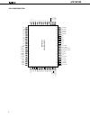
µ pd75p308 2 1 2 3 4 5 6 7 8 9 10 11 12 13 14 15 16 17 18 19 20 21 22 23 24 s12 s13 s14 s15 s16 s17 s18 s19 s20 s21 s22 s23 s24/bp0 s25/bp1 s26/bp2 s27/bp3 s28/bp4 s29/bp5 s30/bp6 s31/bp7 com0 com1 com2 com3 80 79 78 77 76 75 74 73 72 71 70 69 68 67 66 65 s11 s10 s9 s8 s7 s6 s5 s4 s3 s2 s1 s0 reset ...
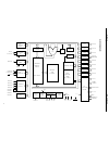
µ pd75p308 3 block diagram p00-p03 p10-p13 p20-p23 p30-p33 /md0-md3 p40-p43 p50-p53 p60-p63 p70-p73 4 4 4 4 4 4 4 4 port0 port1 port2 port3 port4 port5 port6 port7 s0-s23 s24/bp0 -s31/bp7 com0-com3 v -v lco lc2 bias lcdcl/p30 sync/p30 24 8 4 3 lcd controller /driver f lcd reset sp(8) bank general re...
µ pd75p308 4 contents 1. Pin functions ................................................................................................................................. 5 1.1 port pins ......................................................................................................................
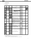
µ pd75p308 5 e-b p00 input int4 p01 input/output sck p02 input/output so/sb0 p03 input/output si/sbi p10 int0 p11 int1 p12 int2 p13 ti0 p20 pto0 p21 — p22 pcl p23 buz p30* 2 p31* 2 p32* 2 md2 p33* 2 md3 p40-43* 2 input/output — p50-p53* 2 input/output — p60 kr0 p61 kr1 p62 kr2 p63 kr3 p70 kr4 p71 kr...
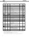
µ pd75p308 6 timer/event counter external event pulse input timer/event counter output clock output fixed frequency output (for buzzer or for trimming the system clock) serial clock input/output serial data output serial bus input/output serial data input serial bus input/output edge detection vecto...
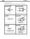
µ pd75p308 7 1.3 pin input/output circuits the following shows a simplified input/output circuit diagram for each pin of the µ pd75p308. Type a (for type e–b) type d (for type e–b, f-a) type b type e–b in v dd p–ch n–ch input buffer of cmos standard data output disable out p–ch n–ch push–pull output...
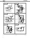
µ pd75p308 8 p-ch type f–a type g – c type g–a type g–b v dd v lc0 v lc0 v lc1 v lc2 seg data/bit port data p-ch n-ch out n-ch v lc1 v lc2 p-ch p-ch n-ch out n-ch v lc0 v lc1 v lc2 p-ch n-ch seg data com data out p-ch n-ch n-ch p-ch data output disable type d type b p.U.R. Enable v dd p–ch in/out p....
µ pd75p308 9 type m-c data output disable p.U.R. Enable v dd p.U.R. In/out p–ch n-ch p.U.R. : pull–up resistor 1.4 notes on using p00/int4 and reset pins in addition to the functions shown in sections 1.1 and 1.2, the p00/int4 and reset pins also have a function to set a test mode (for ic testing) i...
µ pd75p308 10 item µ pd75p308k µ pd75p308gf µ pd75308gf • eprom • prom (one-time model) • mask rom • 0000h-1f7fh • 0000h-1f7fh • 0000h-1f7fh • 8064 x 8 bits • 8064 x 8 bits • 8064 x 8 bits pull-up resistor ports 4, 5 dividing resistor for lcd driving power supply pins 50-53 p30/md0-p33/md3 p30-p33 p...
µ pd75p308 11 pin name function v pp applies voltage when program memory is written/verified (normally, at v dd potential) these pins input clock that updates address when program memory is written/verified. To x2 pin, input signal 180º out of phase in respect to signal to x1 pin. Md0-md3 these pins...
µ pd75p308 12 3.2 program memory write procedure the program memory write procedure is as follows. High-speed program memory write is possible. (1) ground the unused pins through pull-down resistors. The x1 pin must be low. (2) supply 5 v to the v dd and v pp pins. (3) wait for 10 microseconds. (4) ...
µ pd75p308 13 3.3 program memory read procedure the contents of the program memory can be read in the following procedure. (1) ground the unused pins through pull-down resistors. The x1 pin must be low. (2) supply 5 v to the v dd and v pp pins. (3) wait for 10 microseconds. (4) set program memory ad...
µ pd75p308 14 3.4 erasure ( µ pd75p308k only) the contents of the data programmed to the µ pd75p308 can be erased by exposing the window of the program memory to ultraviolet rays. The wavelength of the ultraviolet rays used to erase the contents is about 250 nm, and the quantity of the ultraviolet r...
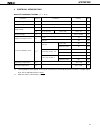
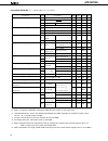
µ pd75p308 15 4. Electrical specifications absolute maximum ratings (t a = 25 ° c) parameter symbol conditions rating unit supply voltage v dd -0.3 to +7.0 v supply voltage v pp -0.3 to +13.5 v v i1 other than ports 4 or 5 -0.3 to v dd +0.3 v v i2 *1 ports 4 and 5 open-drain -0.3 to +11 v output vol...
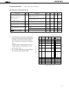
µ pd75p308 16 ceramic *3 oscillation frequency (f xx ) *1 oscillation stabilization after v dd came to min. Time *2 of oscillation voltage range crystal oscilaltion frequency (f xx ) *1 oscillation stabilization time *2 external clock x1 input frequency (f x ) *1 x1 input high-, low-level widths (t ...
µ pd75p308 17 32 32.768 35 khz 1.0 2 s 32 100 khz 5 15 µ s crystal oscillation frequency (f xt ) oscillation stabilization time * external clock xt1 input frequency (f xt ) xt1 input high-, low-level widths (t xth , t xtl ) subsystem clock oscillator circuit characteristics (t a = -10 to +70 ° c, v ...
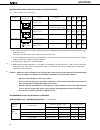
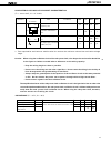
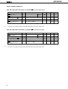
µ pd75p308 18 ports 2, 3 ports 0, 1, 6, 7, reset ports 4, 5 open-drain x1, x2, xt1 ports 2, 3, 4, 5 ports 0, 1, 6, 7, reset x1, x2, xt1 ports 0, 2, 3, i oh = -1ma 6, 7 bias bp0-7 i oh = -100 µ a* 1 ports 0, 2, 3, ports 3, 4, 5 6, 7 i ol = 15ma i ol = 1.6ma sb0, 1 open-drain bp0-7 i ol = 100 µ a* 1 o...
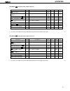
µ pd75p308 19 ac characteristics (t a = -10 to + 70 ° c, v dd = 5v ± 5%) operation other than serial transfer parameter symbol conditions min. Typ. Max. Unit w/main system clock w/subsystem clock int0 kr0-7, int1, 2, 4 t cy f ti t tih, t til t inth, t intl t rsl cpu clock cycle time* 1 (minimum inst...
µ pd75p308 20 serial transfer operation two-line and three-line serial i/o modes (sck: internal clock output) parameter symbol conditions min. Typ. Max. Unit 1600 ns t kcy1 /2-50 ns 150 ns 400 ns 250 ns output output r l = 1k Ω , c l = 100pf* t kcy1 t kh1, t kl1 t sik1 t ksi1 t kso1 sck cycle time s...
µ pd75p308 21 1600 ns t kcy /2 -50 150 ns t kcy /2 ns 0 250 ns t kcy ns t kcy ns t kcy ns t kcy ns sck cycle time sck high-, low-level widths sb0, 1 set-up time (vs. Sck ) sb0, 1 hold time (vs. Sck ) sck sb0, 1 output delay time sck sb0, 1 sb0, 1 sck sb0, 1 low-level width sb0, 1 high-level width sb...
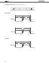
µ pd75p308 22 ac timing test point (excluding x1 and xt1 inputs) test points 0.8 v dd 0.2 v dd 0.8 v dd 0.2 v dd clock timing x1 input v dd –0.5v 0.4 v t xl t xh 1/f x xt1 input v dd –0.5v 0.4 v t xtl t xth 1/f xt ti0 t til t tih 1/f ti ti0 timing.
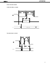
µ pd75p308 23 serial transfer timing three-line serial i/o mode: sck t kl1 t kh1 t kcy1 output data t sik1 t ksi1 t kso1 input data si so two-line serial i/o mode: sck t kl t kh t kcy t sik t ksi sb0,1 t kso.
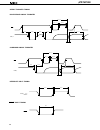
µ pd75p308 24 serial transfer timing bus release signal transfer reset input timing int0, 1, 2, 4 kr0-7 t intl t inth interrupt input timing sck t kl3,4 t kcy3,4 t sik3,4 t ksi3,4 t kso3,4 sb0,1 t kh3,4 t sbk t ksb command signal transfer reset t rsl sck t kl3,4 t kcy3,4 t sik3,4 t ksi3,4 t kso3,4 s...
µ pd75p308 25 released by reset released by interrupt low-voltage data retention characteristics of data memory in stop mode (t a = -10 to +70 ° c) 0 µ s 2 17 /f x ms * 3 ms parameter symbol conditions min. Typ. Max. Unit t srel data retention supply voltage data retention supply current* 1 release ...
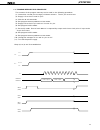
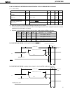
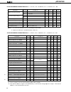
µ pd75p308 26 *1: these symbols are the corresponding µ pd27c256 symbols. 2: the internal address signal is incremented by 1 at the fourth rising edge of x1 input. The internal address is not connected to any pin. Parameter symbol * 1 conditions min. Typ. Max. Unit t as t as t m1s t oes t ds t ds t ...
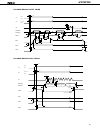
µ pd75p308 27 v pp v dd v dd +1 v dd md0 md1 md2 md3 v pp v dd data input data output data input data input t vps t vds t t ds t dh t t dv t df t ds t ah t as t opw t t m1r t pw t pcr t m1s t m1h t m3s t m3h t vps t vds t t dv t xh t xl t had t dad data output data output t dfr t m3hr t pcr t m3sr t...
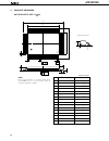
µ pd75p308 28 5. Package drawings n a m f b 64 65 40 k l 80 pin plastic qfp (14 × 20) 80 1 25 24 41 g d c p detail of lead end s q 5°±5° m i h j p80gf-80-3b9-2 item millimeters inches a b c d f g h i j k l 23.6±0.4 14.0±0.2 0.8 0.35±0.10 0.15 20.0±0.2 0.929±0.016 0.039 0.031 0.006 0.031 (t.P.) 0.795...
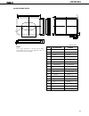
µ pd75p308 29 x80kw-80a-1 item millimeters inches note each lead centerline is located within 0.08 mm (0.003 inch) of its true position (t.P.) at maximum material condition. A b c d e f g h i j k q r s t u w 20.0±0.4 19.0 13.2 14.2±0.4 1.64 2.14 4.064 max. 0.51±0.10 0.08 0.8 (t.P.) 1.0±0.2 c 0.5 0.8...
µ pd75p308 30 6. Recommended soldering conditions it is recommended that µ pd75p308 be soldered under the following conditions. For details on the recommended soldering conditions, refer to information document "semiconductor devices mounting manual" (iei-616). The soldering methods and conditions a...
µ pd75p308 31 hardare ie-75000-r *1 in-circuit emulator for 75k series ie-75001-r ie-75000-r-em *2 emulation board for ie-75000-r and ie-75001-r ep-75308gf-r emulation prove for µ pd75p308gf, provided with 80-pin conversion socket, ev-9200g-80. Pg-1500 prom programmer pa-75p308gf prom programmer ada...
µ pd75p308 32 appendix b. Related documents ★.
µ pd75p308 33 general notes on cmos devices 1 static electricity (all mos devices) exercise care so that mos devices are not adversely influenced by static electricity while being handled. The insulation of the gates of the mos device may be destroyed by a strong static charge. Therefore, when trans...
µ pd75p308 34 [memo] no part of this document may be copied or reproduced in any form or by any means without the prior written consent of nec corporation. Nec corporation assumes no responsibility for any errors which may appear in this document. Nec corporation does not assume any liability for in...

