- DL manuals
- Oki
- Network Card
- MSM9225B
- User Manual
Oki MSM9225B User Manual
Summary of MSM9225B
Page 1
Msm9225b user’s manual can (controller area network) controller oki electric industry co., ltd. Ver. 4.0 july 2001 feul9225b-04 1.
Page 2
Notice 1. The information contained herein can change without notice owing to product and/or technical improvements. Before using the product, please make sure that the information being referred to is up-to-date. 2. The outline of action and examples for application circuits described herein have b...
Page 3
Preface this manual describes the hardware and operation of the msm9225b can controller which conforms to the can protocol specification (bosch, v2.0 part b/active). In this manual, additions and modifications that have been made on the upgrade to the msm9225b from the msm9225 are indicated by “ ” o...
Page 4: Notation
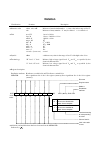
Notation classification notation description ♦ numeric value xxhex, xxh, xxh indicates a hexadecimal number. X: any value in the range of 0 to f xxb indicates a binary number; “b” may be omitted. X: a value 0 or 1 ♦ unit word, w 1 word = 16 bits byte, b 1 byte = 2 nibbles = 8 bits nibble, n 1 nibble...
Page 5
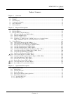
Msm9225b user’s manual contents contents – 1 table of contents chapter 1 overview 1.1 overview..................................................................................................................................................... 1-1 1.2 features...........................................
Page 6
Msm9225b user’s manual contents contents – 2 chapter 4 microcontroller interface 4.1 serial interface ............................................................................................................................................ 4-1 4.2 parallel interface .................................
Page 7: Chapter 1
Chapter 1 overview.
Page 8
Msm9225b user’s manual chapter 1 overview 1 – 1 chapter 1 overview 1.1 overview the msm9225b is a microcontroller peripheral lsi which conforms to the can protocol for high-speed lans in automobiles. 1.2 features • conforms to can protocol specification (bosch, v2.0 part b/active) • maximum of 1 mbp...
Page 9
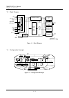
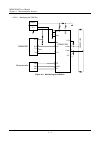
Msm9225b user’s manual chapter 1 overview 1 – 2 1.3 block diagram figure 1-1 block diagram 1.4 configuration example can abs engine controller can can transmission automatic air conditioner can seat-position controller can can outside mirror controller can power window suspension can can bus power s...
Page 10
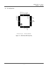
Msm9225b user’s manual chapter 1 overview 1 – 3 1.5 pin configuration connect all v dd pins. Connect all gnd pins. Figure 1-3 44-pin plastic qfp (top view) b b 33 32 31 30 29 28 27 26 25 24 23 1 2 3 4 5 6 7 8 9 10 11 a4 a5 a6 a7 sdo gn d sd i sc l k pr d w /s r cs int ad 2 /d 2 ad 1 /d 1 ad 0 /d 0 m...
Page 11
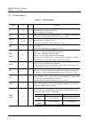
Msm9225b user’s manual chapter 1 overview 1 – 4 1.6 pin descriptions table 1-1 pin description symbol pin type description cs 10 i chip select pin. When “l”, pale, pwr , prd /sr w , sclk and sdo pins (microcontroller interface pins) are valid. When “h”, these pins are invalid. A7-0 41-44, 1-4 i addr...
Page 12
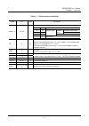
Msm9225b user’s manual chapter 1 overview 1 – 5 table 1-1 pin description (continued) symbol pin type description mode1, 0 29, 30 i microcontroller interface select pins int 11 o interrupt request output pin when an interrupt request occurs, a “l” level is output. This pin automatically outputs a “h...
Page 13: Chapter 2
Chapter 2 register descriptions.
Page 14
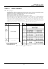
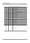
Msm9225b user’s manual chapter 2 register descriptions 2 – 1 chapter 2 register descriptions 2.1 memory space the msm9225b has 256 bytes of memory space for the message memory and control registers. Before starting communication, messages for communication and various control registers must be set. ...
Page 15
Msm9225b user’s manual chapter 2 register descriptions 2 – 2 table 2-1 control register configuration address symbol name 0eh canc can control register 0fh cani can interrupt control register 1eh nmes message box count setting register 1fh btr0 can bus timing register 0 2eh btr1 can bus timing regis...
Page 16
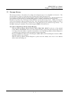
Msm9225b user’s manual chapter 2 register descriptions 2 – 3 2.2 message memory the message memory is the memory for setting and storing messages to be transmitted and received. The message memory consists of 16 message boxes from message box 0 to message box f. It is possible to transmit only the m...
Page 17
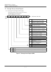
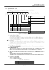
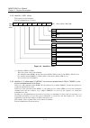
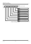
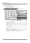
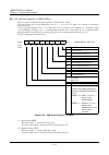
Msm9225b user’s manual chapter 2 register descriptions 2 – 4 2.3 message memory related register 2.3.1 message control register (mcr: x0hex) this register performs various controls for a message. Set this register for each message box. The bit configuration is as follows: msb mma ow trq rcs eir eit ...
Page 18
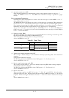
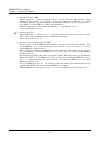
Msm9225b user’s manual chapter 2 register descriptions 2 – 5 (1) automatic transmission: ares if the automatic transmission of the data frame is used for remote frame reception, set this bit to “1”. At reset, the ares bit is set to “0”. The ares bit is invalid if the message is specified as a group ...
Page 19
Msm9225b user’s manual chapter 2 register descriptions 2 – 6 (6) transmission request: trq when a message box is used for transmission, write “1” to this bit from the microcontroller. When transmission ends normally, “0” is written to this bit. This means that the trq bit is “1” during transmission....
Page 20
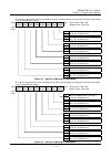
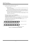
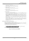
Msm9225b user’s manual chapter 2 register descriptions 2 – 7 2.3.2 identifier 0 (idr0: x1hex) this register sets the frame format, data length code, and a part of the identifier. The bit configuration is as follows: msb idfm dlc3 dlc2 dlc1 dlc0 idb28 idb27 idb26 lsb idr0 (x1hex), r/w: r/w initial va...
Page 21
Msm9225b user’s manual chapter 2 register descriptions 2 – 8 2.3.3 identifier 1 (idr1: x2hex) this register sets the identifier. The bit configuration is as follows: msb idb25 idb24 idb23 idb22 idb21 idb20 idb19 idb18 lsb idr1 (x2hex), r/w: r/w initial value: undefined undefined undefined undefined ...
Page 22
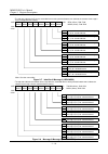
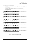
Msm9225b user’s manual chapter 2 register descriptions 2 – 9 * the top rows indicate the id for the extended format setting and the bottom rows indicate the content of message 0 for the standard format setting. Msb idb17 msg07 idb16 msg06 idb15 msg05 idb14 msg04 idb13 msg03 idb12 msg02 idb11 msg01 i...
Page 23
Msm9225b user’s manual chapter 2 register descriptions 2 – 10 * the top rows indicate the id for the extended format setting and the bottom rows indicate the content of message 2 for the standard format setting. Msb idb1 msg27 idb0 msg26 not used msg25 not used msg24 not used msg23 not used msg22 no...
Page 24
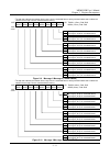
Msm9225b user’s manual chapter 2 register descriptions 2 – 11 * the top rows indicate the content of message 1 for the extended format setting and the bottom rows indicate the content of message 4 for the standard format setting. Msb tmsg17 msg47 tmsg16 msg46 tmsg15 msg45 tmsg14 msg44 tmsg13 msg43 t...
Page 25
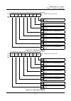
Msm9225b user’s manual chapter 2 register descriptions 2 – 12 * the top rows indicate the content of message 3 for the extended format setting and the bottom rows indicate the content of message 6 for the standard format setting. Msb tmsg37 msg67 tmsg36 msg66 tmsg35 msg65 tmsg34 msg64 tmsg33 msg63 t...
Page 26
Msm9225b user’s manual chapter 2 register descriptions 2 – 13 * the content of message 5 for the extended format setting is shown below. Msb tmsg57 tmsg56 tmsg55 tmsg54 tmsg53 tmsg52 tmsg51 tmsg50 lsb tmsg5 (xbhex), r/w: r/w initial value: undefined undefined undefined undefined undefined undefined ...
Page 27
Msm9225b user’s manual chapter 2 register descriptions 2 – 14 * the content of message 7 for the extended format setting is shown below. Msb tmsg77 tmsg76 tmsg75 tmsg74 tmsg73 tmsg72 tmsg71 tmsg70 lsb tmsg7 (xdhex), r/w: r/w initial value: undefined undefined undefined undefined undefined undefined ...
Page 28
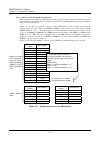
Msm9225b user’s manual chapter 2 register descriptions 2 – 15 notes on identifier (id) and message priority • priority of message a message has the priority determined by the identifier setting. To determine priority, identifiers of messages are compared from the higher bit, and the identifier (set ...
Page 29
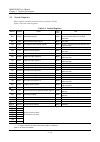
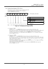
Msm9225b user’s manual chapter 2 register descriptions 2 – 16 2.4 control registers these registers listed below control various operations of can. Table 2-4 lists the control registers. Table 2-4 control registers address symbol name initial value r/w 0eh canc can control register 01hex bits 4, 5 a...
Page 30
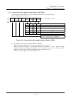
Msm9225b user’s manual chapter 2 register descriptions 2 – 17 2.4.1 can control register (canc: 0ehex) this register controls the operation of can. The bit configuration is as follows: msb not used rxf txf cana sync not used tirs init lsb canc (0ehex), *r/w: r/w initial value: 0 0 0 0 0 0 0 1 0 rele...
Page 31
Msm9225b user’s manual chapter 2 register descriptions 2 – 18 (2) search for the transmit identifier: tirs when this bit is set, the identifiers are scanned starting from the message box 0 up to last message box specified by nmes, the messages with the transmission request bit trq set to “1” are det...
Page 32
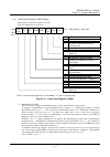
Msm9225b user’s manual chapter 2 register descriptions 2 – 19 2.4.2 can interrupt control register (cani: 0fhex) this register controls can interrupts. The bit configuration is as follows: msb meint ief irf itf not used einte eintr eintt lsb cani (0fhex), *r/w: r/w initial value: 0 0 0 0 0 0 0 0 0 t...
Page 33
Msm9225b user’s manual chapter 2 register descriptions 2 – 20 (3) error interrupt output enable: einte when an error occurs, this bit is used to output error interrupt signal inte from interrupt pin int . When einte is “0”, an error interrupt signal is not output from the interrupt pin. When einte i...
Page 34
Msm9225b user’s manual chapter 2 register descriptions 2 – 21 2.4.3 message box count setting register (nmes: 1ehex) this is a register to set the number of message boxes to be used. A maximum of 16 message boxes can be set, with message box numbers 0 to f. Writing to nmes is enabled when initialize...
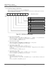
Page 35
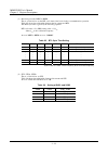
Msm9225b user’s manual chapter 2 register descriptions 2 – 22 (1) baud rate prescaler: brp5 to brp0 this is a 6-bit field to set the btl cycle time of the basic clock for communication operation. Table 2-5 shows the relationship between the bit content and btl. The btl cycle time is given by the fol...
Page 36
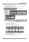
Msm9225b user’s manual chapter 2 register descriptions 2 – 23 2.4.5 can bus timing register 1 (btr1: 2ehex) this register sets the sampling point used for bus timing. Writing to the btr1 bit is enabled, when the init bit of the can control register (canc: 0ehex) is “1”. The bit configuration is as f...
Page 37
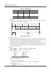
Msm9225b user’s manual chapter 2 register descriptions 2 – 24 table 2-8 tseg2 setting tseg22 tseg21 tseg20 tseg2 0 0 0 1 × btl cycle 0 0 1 2 × btl cycle • • • • • • • • • • • • 1 1 0 7 × btl cycle 1 1 1 8 × btl cycle (3) bit timing bit timing is set by can bus timing registers 0 and 1 (btr0, 1). Fig...
Page 38
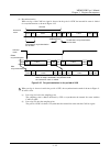
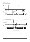
Msm9225b user’s manual chapter 2 register descriptions 2 – 25 (4) resynchronization when an edge of the can bus signal is detected in the period of sjw, the internal bit status is shifted for resynchronization as shown in figure 2-25. Internal bit status period where resynchronization can be done ts...
Page 39
Msm9225b user’s manual chapter 2 register descriptions 2 – 26 tseg2 sync sjw1 tseg1 sjw2 sync sjw1 tseg1 tseg2 sjw2 sjw sync sjw1 tseg1 tseg2 sjw2 sync tseg1 tseg2 sjw2 can bus signal before resynchronization after resynchronization the sampling point is shifted by sjw. Sjw1 sampling point sampling ...
Page 40
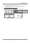
Msm9225b user’s manual chapter 2 register descriptions 2 – 27 2.4.6 communication input/output control register (tioc: 2fhex) this register sets the input/output mode and output driver format of output pins tx0 and tx1. Writing to the tioc bit is enabled when the init bit of the can control register...
Page 41
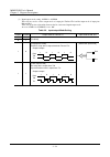
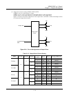
Msm9225b user’s manual chapter 2 register descriptions 2 – 28 (1) input/output mode setting: ocmd1 to ocmd0 these bits are used to set the output mode of output pins tx0 and tx1 and the input mode of input pins rx0 and rx1. Table 2-9 shows the relationship between the bit content and input/output mo...
Page 42
Msm9225b user’s manual chapter 2 register descriptions 2 – 29 (2) output driver format setting: ocpol, octn, octp ocpol is used to set the polarity of output. Octn is used to set the open drain mode of the nch transistor of the output driver. Octp is used to set the open drain mode of the pch transi...
Page 43
Msm9225b user’s manual chapter 2 register descriptions 2 – 30 2.4.7 group message register (gmr0: 3ehex, gmr1: 3fhex) these are registers to set the group message function. Group message function if the group message function is used, a part of an identifier can be masked. This can increase the numb...
Page 44
Msm9225b user’s manual chapter 2 register descriptions 2 – 31 2.4.8 group message mask register (gmsk) these are registers to mask the identifier of the message box specified by the group message registers gmr0 and gmr1. Using mnid28 to mnid0 (n = 0, 1), set the bits to mask the identifier. Setting ...
Page 45
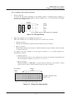
Msm9225b user’s manual chapter 2 register descriptions 2 – 32 notes on how to set the group message function when setting the group message (gm) function in the message box that selects the extended format as a frame format, specify the message box numbers consecutively, beginning with the message b...
Page 46
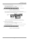
Msm9225b user’s manual chapter 2 register descriptions 2 – 33 2.4.9 standby control register (stby: 8ehex) this register is used for setting the stop mode and the sleep mode. A “0” is read after the stop or sleep mode is terminated. The bit configuration is as follows: msb not used not used not used...
Page 47
Msm9225b user’s manual chapter 2 register descriptions 2 – 34 2.4.10 can control register 2 (canc2: 8fhex) this is a register to control bus off release and error counter operation. The bit configuration is shown below. At reset, this register is set to “0000 0000”. Msb not used not used not used rs...
Page 48
Msm9225b user’s manual chapter 2 register descriptions 2 – 35 2.4.11 communication message box number register (tmn: 9ehex) the message box number when a message is transmitted/received is stored in this register. The bit configuration is as follows: msb not used not used not used not used trsn3 trs...
Page 49
Msm9225b user’s manual chapter 2 register descriptions 2 – 36 2.4.12 can status register (cans: 9fhex) this is a register to indicate the error status of the msm9225b. Bit 6 to bit 4 are flags for the transmitter and bit 1 and bit 0 are for the receiver, and this register is read-only. The bit confi...
Page 50
Msm9225b user’s manual chapter 2 register descriptions 2 – 37 2.4.13 transmit error counter (tec: aehex) tec is a register to indicate the transmit error counter value. This register is read-only. At reset or when in the bus off state, tec is set to “0000 0000”. The bit configuration is shown below....
Page 51
Msm9225b user’s manual chapter 2 register descriptions 2 – 38 2.4.15 can status register 2 (cans2: behex) this is a register to indicate the error contents for when an error occurs. If an error occurs, the corresponding flag is set to “1”. It is set to “0” when “0” is written to it from the microcon...
Page 52
Msm9225b user’s manual chapter 2 register descriptions 2 – 39 (3) acknowledgment error flag: ack this bit becomes “1” when an acknowledgment error occurs. At reset or after release of the bus off state, this bit becomes “0”. (4) crc error flag: crc this bit becomes “1” when a crc error occurs. At re...
Page 53: Chapter 3
Chapter 3 operational description.
Page 54
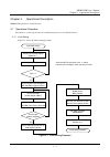
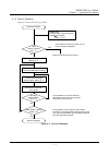
Msm9225b user’s manual chapter 3 operational description 3 – 1 chapter 3 operational description msm9225b operation is described below. 3.1 operational procedure procedures to set and operate various communication protocols are indicated below. 3.1.1 initial setting figure 3-1 shows the initial sett...
Page 55
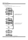
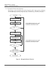
Msm9225b user’s manual chapter 3 operational description 3 – 2 3.1.2 transmit procedure figure 3-2 shows the transmit procedure. * see appendix c “transmission failure of msm9225b” for transmission operation. Start transmit setting set mma bit of the message control register (x0hex) to 1 read mma bi...
Page 56
Msm9225b user’s manual chapter 3 operational description 3 – 3 3.1.3 receive procedure figure 3-3 shows the receive procedure. Receive procedure yes (msm9225b) interrupt signal is generated when reception is complete int pin h to l set irf bit of cani register (0fhex) to 0 verify received message bo...
Page 57
Msm9225b user’s manual chapter 3 operational description 3 – 4 3.1.4 message box rewrites during operation the procedure to rewrite the identifier (id) and data length code (dlc) during operation, excluding the time that initial settings are made for the message boxes, is indicated below. The number...
Page 58
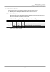
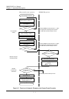
Msm9225b user’s manual chapter 3 operational description 3 – 5 3.1.5 remote frame operation the following two methods are available for transmission after remote frame reception. (1) automatic response: automatically transmit preset message data in message box (2) manual response: set message data a...
Page 59
Msm9225b user’s manual chapter 3 operational description 3 – 6 microcontroller (user) operation msm9225b operation start automatic response remote transmission complete set mma bit of message control register (x0hex) to 1 mma = 1? Canc register’s (0fhex) itf is 1? Yes no no yes read mma bit set the ...
Page 60
Msm9225b user’s manual chapter 3 operational description 3 – 7 3.1.5.2 manual response in this method, after remote frame reception, the transmit data is set and then transmission begins. Table 3-2 lists the settings of the message control register. * see appendix c “transmission failure of msm9225b...
Page 61
Msm9225b user’s manual chapter 3 operational description 3 – 8 microcontroller (user) operation msm9225b operation start manual response mma = 1? Yes no remote frame received? Yes no data frame transmission message reception generates interrupt int pin h to l remote reception transmit data setting r...
Page 62: Chapter 4
Chapter 4 microcontroller interface.
Page 63
Msm9225b user’s manual chapter 4 microcontroller interface 4 – 1 chapter 4 microcontroller interface there are two methods of interfacing to the microcontroller. (1) synchronous serial interface (serial mode) (2) parallel bus interface (parallel mode) each interface is selected with the mode1 and mo...
Page 64
Msm9225b user’s manual chapter 4 microcontroller interface 4 – 2 a0 a1 a2 a3 a4 a5 a6 a7 d0 d1 d2 d3 d4 d5 d6 d7 d0 d1 d2 d3 d4 d5 d6 d7 * * * * * * * * * * * * * * * * * * * * * * * * sdi sclk cs sdo sr w swait address reception internal processing interval data reception internal processing interv...
Page 65
Msm9225b user’s manual chapter 4 microcontroller interface 4 – 3 4.2 parallel interface the following three types of parallel interfaces are available. (1) address/data separate bus type, no address latch signal (2) address/data separate bus type, with address latch signal (3) multiplexed bus type f...
Page 66
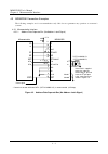
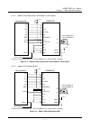
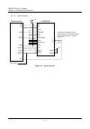
Msm9225b user’s manual chapter 4 microcontroller interface 4 – 4 4.3 msm9225b connection examples the following examples are for recommendation only. Oki does not guarantee any operation on customer’s systems. 4.3.1 microcontroller interface 4.3.1.1 address/data separate bus (no address latch signal...
Page 67
Msm9225b user’s manual chapter 4 microcontroller interface 4 – 5 4.3.1.2 address/data separate bus (with address latch signal) msm9225b microcontroller int cs pale prd /sr w pwr prdy /swait a7-0 ad7-0/d7-0 sdo sdi xt xt int cs rd wr wait a7-0 d7-0 reset 11 10 27 9 26 16 4-1, 44-41 38-31 5 7 8 25 res...
Page 68
Msm9225b user’s manual chapter 4 microcontroller interface 4 – 6 4.3.1.4 serial interface msm9225b microcontroller int cs pale prd /sr w pwr prdy /swait a7-0 ad7-0/d7-0 sdo sdi xt xt r/ w wait reset 11 10 27 9 26 16 4-1, 44-41 38-31 5 7 8 25 reset signal 13 14 30 29 10 k Ω +5 v reset mode0 sclk mode...
Page 69
Msm9225b user’s manual chapter 4 microcontroller interface 4 – 7 4.3.2 can bus interface 4.3.2.1 electrically isolated from bus transceiver (pca82c250) msm9225b r × 1 19 6.2 k Ω 5.1 k Ω r × 0 18 t × 0 22 t × 1 23 open pca82c250 v cc 3 canh 7 rs 8 vref 5 open rxd txd 6n137 o.P. Cath 4 open 1 open 3 g...
Page 70
Msm9225b user’s manual chapter 4 microcontroller interface 4 – 8 4.3.2.3 monitoring the can bus msm9225b 23 open pca82c252 canh 11 canl 12 can bus l ine v cc 10 gnd 13 rth 8 rtl 9 rxd 3 inh 1 txd 2 en 6 nerr 4 stb 5 port port port t × 0 t × 1 r × 0 22 18 r × 1 19 battery +5 v microcontroller ba t 14...
Page 71: Chapter 5
Chapter 5 electrical characteristics.
Page 72
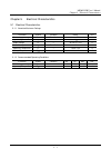
Msm9225b user’s manual chapter 5 electrical characteristics 5 – 1 chapter 5 electrical characteristics 5.1 electrical characteristics 5.1.1 absolute maximum ratings parameter symbol condition rating unit power supply voltage v dd ta = 25°c –0.3 to +7.0 v input voltage v i — –0.3 to v dd +3.0 v outpu...
Page 73
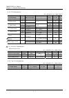
Msm9225b user’s manual chapter 5 electrical characteristics 5 – 2 5.1.3 dc characteristics (v dd = 4.5 to 5.5 v, ta = –40 to +125°c) parameter symbol applicable pin condition min. Max. Unit “h” input voltage v ih applies to all inputs — 0.8v dd v dd +0.3 v “l” input voltage v il applies to all input...
Page 74
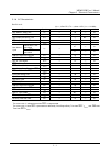
Msm9225b user’s manual chapter 5 electrical characteristics 5 – 3 5.1.6 ac characteristics parallel mode (v dd = 4.5 to 5.5 v, ta = –40 to +125°c, f osc = 16 mhz) parameter symbol condition min. Max. Unit ale address setup time t as — 10 — ns ale address hold time t ah — 10 — ns prd output data dela...
Page 75
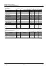
Msm9225b user’s manual chapter 5 electrical characteristics 5 – 4 serial mode (v dd = 4.5 to 5.5 v, ta = –40 to +125°c, f osc = 16 mhz) parameter symbol condition min. Max. Unit cs setup time t cs — 10 — ns cs hold time t ch — 8t — ns sclk cycle t cp — 167 — ns sclk pulse width t cw — 83 — ns sdi se...
Page 76
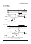
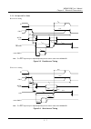
Msm9225b user’s manual chapter 5 electrical characteristics 5 – 5 5.2 timing diagrams 5.2.1 separate bus mode read access timing t cyc t rah t wrdh t rdh t arldly t wrdyl t rdly t rs t hrc cs a7-0 ad7-0/ d7-0 prd /sr w prdy /swait t arddly note: the prdy signal may be output depending on the interna...
Page 77
Msm9225b user’s manual chapter 5 electrical characteristics 5 – 6 5.2.2 separate bus/address latch mode read access timing t cyc t ah t wrdh t arldly t wrdyl t rdly t waleh t hrc cs a7-0 ad7-0/ d7-0 prd /sr w prdy /swait t rdh t hra t as pale don’t care t arddly t rs note: the prdy signal may be out...
Page 78
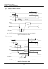
Msm9225b user’s manual chapter 5 electrical characteristics 5 – 7 5.2.3 multiplexed bus mode read access timing t cyc t wrdh t arldly t wrdyl t rdly t waleh t hrc cs ad7-0/ d7-0 prd /sr w prdy /swait t rdh t hra t as pale t ah t arddly t rs note: the prdy signal may be output depending on the intern...
Page 79
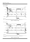
Msm9225b user’s manual chapter 5 electrical characteristics 5 – 8 5.2.4 serial mode read access timing note: the swait signal will be output during the interval between address and data transfers. Figure 5-7 read access timing write access timing note: the swait signal will be output during the inte...
Page 80
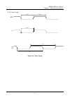
Msm9225b user’s manual chapter 5 electrical characteristics 5 – 9 5.2.5 other timing t wrstl reset t wrsth t wintl int t clkcy clk (xt) t clkcy figure 5-9 other timing.
Page 81: Appendixes
Appendixes.
Page 82
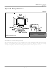
Msm9225b user’s manual appendixes a – 1 appendix a package dimensions (unit: mm) qfp44-p-910-0.80-2k mirror finish package material epoxy resin lead frame material 42 alloy pin treatment solder plating ( ≥ 5µm) package weight (g) 0.41 typ. 5 rev. No./last revised 4/nov. 28, 1996 notes for mounting t...
Page 83
Msm9225b user’s manual appendixes a – 2 appendix b msm9225b memory map the following is the memory map of the entire memory space of the msm9225b. The symbols ‘mn’ (for example, m0mcr, m0msg0, m0idr2, etc., n = 0 to 15) correspond to the number of the respective message box among the message boxes 0...
Page 84
Msm9225b user’s manual appendixes a – 3 name abbreviated name address [h] standard extended standard extended r/w access value at reset [h] 0020 message control register m2mcr r/w 8 00 0021 identifier 0 m2idr0 r/w 8 undefined 0022 identifier 1 m2idr1 r/w 8 undefined 0023 message 0 identifier 2 m2msg...
Page 85
Msm9225b user’s manual appendixes a – 4 name abbreviated name address [h] standard extended standard extended r/w access value at reset [h] 0040 message control register m4mcr r/w 8 00 0041 identifier 0 m4idr0 r/w 8 undefined 0042 identifier 1 m4idr1 r/w 8 undefined 0043 message 0 identifier 2 m4msg...
Page 86
Msm9225b user’s manual appendixes a – 5 name abbreviated name address [h] standard extended standard extended r/w access value at reset [h] 0060 message control register m6mcr r/w 8 00 0061 identifier 0 m6idr0 r/w 8 undefined 0062 identifier 1 m6idr1 r/w 8 undefined 0063 message 0 identifier 2 m6msg...
Page 87
Msm9225b user’s manual appendixes a – 6 name abbreviated name address [h] standard extended standard extended r/w access value at reset [h] 0080 message control register m8mcr r/w 8 00 0081 identifier 0 m8idr0 r/w 8 undefined 0082 identifier 1 m8idr1 r/w 8 undefined 0083 message 0 identifier 2 m8msg...
Page 88
Msm9225b user’s manual appendixes a – 7 name abbreviated name address [h] standard extended standard extended r/w access value at reset [h] 00a0 message control register m10mcr r/w 8 00 00a1 identifier 0 m10idr0 r/w 8 undefined 00a2 identifier 1 m10idr1 r/w 8 undefined 00a3 message 0 identifier 2 m1...
Page 89
Msm9225b user’s manual appendixes a – 8 name abbreviated name address [h] standard extended standard extended r/w access value at reset [h] 00c0 message control register m12mcr r/w 8 00 00c1 identifier 0 m12idr0 r/w 8 undefined 00c2 identifier 1 m12idr1 r/w 8 undefined 00c3 message 0 identifier 2 m1...
Page 90
Msm9225b user’s manual appendixes a – 9 name abbreviated name address [h] standard extended standard extended r/w access value at reset [h] 00e0 message control register m14mcr r/w 8 00 00e1 identifier 0 m14idr0 r/w 8 undefined 00e2 identifier 1 m14idr1 r/w 8 undefined 00e3 message 0 identifier 2 m1...
Page 91
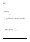
Msm9225b user’s manual appendixes a – 10 appendix c msm9225b user’s manual contents of revision from 3rd version to 4th version • 2.2 message memory (4th ver) “note when reading message memory related register” was added. • 2.4.1 (5) transmission flag: txf (4th ver) “txf becomes “0” when transmissio...
Page 92: Msm9225B
Msm9225b user’s manual version 1.0: may 2000 version 2.0: september 2000 version 3.0: february 2001 version 4.0: july 2001 2001 oki electric industry co., ltd. Feul9225b-04.

