- DL manuals
- Oki
- All in One Printer
- OKIFAX4550
- Maintenance Manual
Oki OKIFAX4550 Maintenance Manual
Summary of OKIFAX4550
Page 1
41309401th rev.4 1 / 592 okifax4550/ okioffice87 maintenance manual 2001-05-08 rev.4 oki data corporation.
Page 2
41309401th rev.4 2 / rev.No. Date corrected items person in section page description of change charge 1 2000-03 issue e3 endo 2 2000-07-21 change the appendix d. Ef oba 3 2000-10-31 add the okioffice87, etc. Ef saito 4 2001-05-08 change the appendix d. Np3 oba document revision history.
Page 3
41309401th rev.4 3 / this manual is intended to be used for installing and maintaining okifax4550/okioffice87 facsimile transceiver. Maintenance of the okifax4550/okioffice87 is assumed to be conducted at the following levels: • assembly-level maintenance for mechanical portions • unit-level mainten...
Page 4
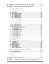
41309401th rev.4 4 / contents 1. General information ................................................................................. 8 1.1 general performance ........................................................................................................... 8 1.2 general user's functions ...
Page 5
41309401th rev.4 5 / 4.3.16 hopping shaft assembly ......................................................................................... 175 4.3.17 paper sensor e, paper sensor exit and toner sensor assembly ......................... 176 4.3.18 printer unit .........................................
Page 6
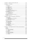
41309401th rev.4 6 / 8. Dipswitchs setting tables for en9/inu ncu boards ...................... 261 appendix a pc board descriptions and operation ........................... 271 1. Unit configuration and block diagram ....................................................................................
Page 7
41309401th rev.4 7 / appendix e board layout and parts list .............................................. 456 appendix f pc-loading .................................................................................. 516 1. General ........................................................................
Page 8
41309401th rev.4 8 / 1. General information 1.1 general performance (1) type of appearance • desktop type (2) applicable lines • public switched telephone network (pstn) • private branch exchange (pbx) • isdn (integred service digital network) • fax2net internet fax (via pstn) note: isdn and interne...
Page 9
41309401th rev.4 9 / (12) scanning resolution a) horizontal: • 300 dot/inch note 1: in the local copy mode at standard (std) resolutions, the dpi conversion is done from 300 dot/inch to 200 dot/inch. 2: 600 dpi × 15.4 line/mm: copy is available for okioffice87. B) vertical: transmission mode: 3.85 l...
Page 10
41309401th rev.4 10 / (20) modem • itu-t rec. V.29: 9600 bps for use on point-to-point 4-wire leased telephone type curcuits. • itu-t rec. V.27 ter: 4800 bps modem for use in pstn (public switched telephone network) • itu-t rec. V.21 channel 2: 300 bps duplex modem for pstn • itu-t rec. V.17: 2-wire...
Page 11
41309401th rev.4 11 / 1.2 general user's functions (1) transmit mode • automatic transmit mode • manual transmit mode (2) receive mode • automatic receive mode • manual receive mode • tel/fax automatic switchover mode • tad mode • memory only receive mode • forwarding mode • pc receive mode (this fu...
Page 12
41309401th rev.4 12 / (21) g3 sequential broadcast (memory) • broadcast mode 90 stations at maximum for okifax4550 120 stations at maximum for okioffice87 • delayed broadcast mode (22) no paper/no toner reception (23) memory-only reception (memory reception even if paper does not run out) (24) disti...
Page 13
41309401th rev.4 13 / (44) pc interface • standard: okioffice87 • option: okifax4550 note: hardware is mounted. (45) language selection • 2 languages (lcd and reports) (46) reports • activity report • active memory files report • protocol report • message confirmation report (single address and mult...
Page 14
41309401th rev.4 14 / 1.3 general maintenance functions 1) local tests (1) self-diagnosis • cpu rom/ram check • flash memory check (program, language, default) • ram check • print test (2) sensor calibration (adjustment of scanning level) (3) leds test (4) tone send test (when ncu board is installed...
Page 15
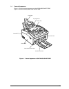
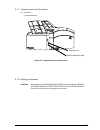
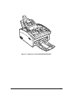
41309401th rev.4 15 / tray-paper tray-document cover-top cover-front stacker-document cover manual document cover-main case-ope (t) figure 1.1 general appearance of okifax4550/okioffice87 1.4 general appearance figure 1.1 shows the general appearance of the okifax4550/okioffice87. Figure 1.2 shows t...
Page 16: 4550
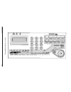
41309401th rev.4 16 / figure 1.2 control panel of okifax 4550 unique 8.5" a4 b5 a5 okifax auto rec search auto dial hyphen redial hook v.Request photo ex fine fine std light normal dark alarm stop start yes yes no no oki * 0 # abc def jkl mno ghi tuv wxyz pqrs 7 8 9 4 5 6 1 2 3 select function delay...
Page 17
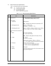
41309401th rev.4 17 / 1.5 basic performance specifications table 1.1 shows basic performance specifications. Note: tf: technical function setting fp: function program setting ot: one-touch key pressed f: select function key pressed table 1.1 (1/11) basic performance specifications no. Item specifica...
Page 18
41309401th rev.4 18 / table 1.1 (2/11) basic performance specifications no. Item specifications document width communication mode/paper width effective reading width copy size iso a4 (210 mm) [int'l/ftz] g3/a4 a4 208 mm for tx 203.2 mm for local copy (208 mm for local copy with horizontal reduction ...
Page 19
41309401th rev.4 19 / table 1.1 (3/11) basic performance specifications no. Item specifications 9 recording paper or sheet 10 recording paper cassette for tray-paper: 1) type: plain paper cut (bond paper) 2) size: iso a4 (210 mm × 297 mm) na letter (215.9 mm × 279.4 mm)/(8.5 inch × 11 inch) na legal...
Page 20
41309401th rev.4 20 / table 1.1 (4/11) basic performance specifications no. Item specifications 2) guaranteed printing area printing area el pl b t l r pw ew recording paper feed direction 1) printable area pl 11 279.4 11.7 297 14 355.6 inch mm inch mm inch mm na letter size iso a4 size 14 inch lega...
Page 21
41309401th rev.4 21 / table 1.1 (5/11) basic performance specifications no. Item specifications 13 scanning resolution 14 image scanning method 15 contrast control 16 recording resolution 17 recording system 18 skew of recording paper 19 copy darkness 20 copy uniformity horizontal: • 300 dot/inch no...
Page 22
41309401th rev.4 22 / the fax can detect the no-paper condition by a photosensor. When the paper has run out in the local copy operation, the scanning will stop with “paper out/jam” on the lcd and an alarm led turns on without an alarm tone. When the paper has run out while a message is being receiv...
Page 23
41309401th rev.4 23 / 1) itu-t rec. T.30 2) oki data special protocol high-speed protocol the t.30 protocol signal from the transmitting station is sent at message transmission speed instead of 300 bps. (this function is disable when the h/modem rate is set to 9.6 kbit/s by tf no.13) note : in hihg-...
Page 24
41309401th rev.4 24 / 37 power supply unit and power consumption of the machine table 1.1 (9/11) basic performance specifications no. Item specifications the following four modes are supported: 1) pc local printer function 2) pc scanner function 3) pc faxmodem function 4) location programing functio...
Page 25
41309401th rev.4 25 / table 1.1 (10/11) basic performance specifications no. Item specifications • humidity the machine will operate as specified at relative humidities in the range of 20 percent to 80 percent (non-condensing). Operation outside this range will be subject to the limitations shown in...
Page 26
41309401th rev.4 26 / table 1.1 (11/11) basic performance specifications no. Item specifications 1) ac power cord × 1 2) i/d unit × 1 (already installed) 3) toner cartridge × 1 4) tray - paper 5) tray - document 6) document stacker × 1 7) line cord × 1 8) one touch sheet × 1 (already installed) 9) u...
Page 27
41309401th rev.4 27 / the transmitter sends a call-back message to the receiver only when the receiver does not respond to voice request of the transmitter. The fax can transmit a programmed alphanumeric message, such as company’s name, consisting of up to 32 characters. * (outside only) received ts...
Page 28
41309401th rev.4 28 / no. Item specifications 11 telephone directory 12 configuration report 13 active memory files 14 protocol dump (g3) 15 self-diagnosis report 16 log report 17 protocol dump (g4) 18 g4 log report this directory is printed manually. (report printing + 4) this report is printed man...
Page 29: Message Confirmation
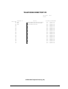
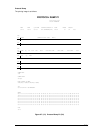
41309401th rev.4 29 / message confirmation 07/01/2000 08:05 id=oki date s,r-time distant station id mode pages result 07/01 00'20" oki fax calling 02 ok 0000 message confirmation report (mcf).
Page 30: Message Confirmation
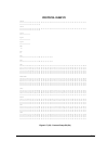
41309401th rev.4 30 / message confirmation 07/01/2000 17:05 id=oki date s,r-time distant station id mode pages result 07/01 00'20" b.C. 01 comp. 60a0 image in mcf with memory tx 150 km.
Page 31: Activity Report
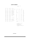
41309401th rev.4 31 / activity report 07/01/2000 17:05 id=oki total time tx=08:22' rx=17:30' date time s,r-time distant station id mode pages result 06/29 10:00 01'20" oki fax tx 02 ok 0000 06/29 10:10 01'00" 0485 88 3385 tx 00 stop 9080 06/29 10:30 00'20" ods takasaki tx 00 no 90c1 06/29 12:05 01'2...
Page 32: Active Memory Files
41309401th rev.4 32 / active memory files 07/01/2000 17:05 id=odc reception entries pages 05 20 personal box box no. Mode entries pages 01 conf 03 20 02 conf 01 02 05 poll 01 05 polling tx/rx date time distant station id mode pages poll tx 03 07/02 12:05 oki poll rx transmission date time didtant st...
Page 33
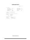
41309401th rev.4 33 / configuration print conditions 1) setting by user two pages shall be printed out. Setting only is printed on the first page and dial parameter setting, system data prg. And fax2net/isdn registration.Are printed on the second page. 2) setting by service persons printed as the th...
Page 34
41309401th rev.4 34 / 30) 36: ced send “on,” “off” are printed. 31) 37: fax2net function “on,” “off” are printed. 32) 38: top feed “-10mm,” “-9mm,” “ —, “ 0mm,” “+1mm’” — “+9m” 39: bottom feed “-2mm,” —, “0mm,” “+1mm” —”+10mm” 33) 40: g3/g4 learning “on,” and “off” are printed. Left blank when no is...
Page 35: Configuration P1
41309401th rev.4 35 / report image configuration p1 02/14/2000 12:00 id=ods function list 01:mcf (single-loc.) 02:mcf (multi-loc.) 03:err.Report (mcf) off on on 04:image in mcf 05:sender id. 06:monitor volume on on low 07:buzzer volume 08:closed network 09:tx mode default middle off std/normal 10:t/...
Page 36: Configuration P2
41309401th rev.4 36 / configuration p2 02/14/2000 12:00 id=ods dial parameter redial tries 3 try redial interval 3 min dial tone detect off busy tone detect on mf(tone)/dp(pulse) mf pulse dial rate 10 pps pulse make ratio 39% pulse dial type n mf(tone) duration 100ms pbx line off pbx type normal aut...
Page 37: Configuration P3
41309401th rev.4 37 / configuration p3 02/14/2000 12:00 id=ods function list 01:service bit 02:monitor cont. 03:country code on on ger 04:time/date print 05:tsi print 06:tad mode off on type2 07:real time dial 08:tel/fax switch 09:mdy/dmy type2 on mdy 10:long doc. Scan 11:tone for echo 12:mh only on...
Page 38
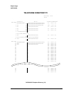
41309401th rev.4 38 / telephone directory print conditions formats of okifax4550, and okioffice87 shall be made common. Number of ots okifax4550 10 okioffice87 number of ads 70 100 number of groups 5 maximum number of digits of ot/ad tel no. 32 40 maximum number of digits of ot or tel no. 32 40 maxi...
Page 39: Telephone Directory P1
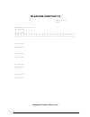
41309401th rev.4 39 / report image okifax4550 telephone directory p1 02/14/2000 12:00 id=ods location id tel no. G3-echo/g3-rate/mode one touch 1 abcdefghijklmno 12345678901234567890123456789012 on / 33.6k / g4 or 12345678901234567890123456789012 2 ot2 123456789012345678901234567890 off / 9.6k / g3 ...
Page 40: Telephone Directory P2
41309401th rev.4 40 / telephone directory p2 02/14/2000 12:00 id=ods location id tel no. G3-echo/g3-rate/mode auto dial 46 ad46 12345678901234567890123456789012 on / 33.6k / g4 47 ad47 123456789012345678901234567890 on / 33.6k / g4 48 ad48 12345678901234567890 on / 33.6k / g4 49 on / 33.6k / g4 50 o...
Page 41: Telephone Directory P3
41309401th rev.4 41 / telephone directory p3 02/14/2000 12:00 id=ods group number = #1 #2 #3 #4 #5 1 2 3 4 5 6 7 8 9 10 01 02 03 04 05 06 07 08 09 10 11 12 13 14 15 16 17 18 19 20 21 22 23 24 25 26 27 28 29 30 31 32 33 34 35 36 37 38 39 40 41 42 43 44 45 46 47 48 49 50 51 52 53 54 55 56 57 58 59 60 ...
Page 42: Telephone Directory P1
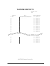
41309401th rev.4 42 / okioffice87 telephone directory p1 02/14/2000 12:00 id=ods location id tel no. G3-echo/g3-rate/mode one touch 1 abcdefghijklmno 12345678901234567890123456789012 on / 33.6k / g4 or 12345678901234567890123456789012 2 ot2 123456789012345678901234567890 off / 9.6k / g3 or 3 ot3 123...
Page 43: Telephone Directory P2
41309401th rev.4 43 / telephone directory p2 02/14/2000 12:00 id=ods location id tel no. G3-echo/g3-rate/mode auto dial 46 ad46 12345678901234567890123456789012 on / 33.6k / g4 47 ad47 123456789012345678901234567890 on / 33.6k / g4 48 ad48 12345678901234567890 on / 33.6k / g4 49 on / 33.6k / g4 50 o...
Page 44: Telephone Directory P3
41309401th rev.4 44 / telephone directory p3 02/14/2000 12:00 id=ods group number = #1 #2 #3 #4 #5 1 2 3 4 5 6 7 8 9 10 01 02 03 04 05 06 07 08 09 10 11 12 13 14 15 16 17 18 19 20 21 22 23 24 25 26 27 28 29 30 31 32 33 34 35 36 37 38 39 40 41 42 43 44 45 46 47 48 49 50 51 52 53 54 55 56 57 58 59 60 ...
Page 45
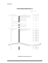
41309401th rev.4 45 / protocol dump p1 12/24/1998 19:00 id=oki takasaki date time s,r-time distant station id mode pages result 12/24 18:56 00'33" 123456789012345678901234 tx 002 ok 0000 fcf tx nss pps_mps pps_eop dcn rx nsf dis cfr mcf mcf tx rx tx rx tx rx transmitted frame dis 00 00 00 00 00 00 0...
Page 46
41309401th rev.4 46 / protocol dump p2 12/24/1998 19:00 id=oki takasaki received frame dis ff c8 01 00 73 17 22 00 00 00 00 00 00 00 00 00 00 00 00 00 dtc 00 00 00 00 00 00 00 00 00 00 00 00 00 00 00 00 00 00 00 00 dcs 00 00 00 00 00 00 00 00 00 00 00 00 00 00 00 00 00 00 00 00 nsf ff c0 04 00 00 84...
Page 47: Broadcast Entry Report
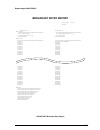
41309401th rev.4 47 / report image (okifax4550) broadcast entry report 02/14/2000 12:00 id=ods location id location id one touch 1=12345678901234567890123456789012 2=12345678901234567890123456789012 3=oki data corp. 4=s-ishika@okidata.Co.Jp 5=timomo@alles.Or.Jp 6=0273265978 7=0273261447 10=027326598...
Page 48: Broadcast Entry Report
41309401th rev.4 48 / report image (okioffice87) broadcast entry report 02/14/2000 12:00 id=ods location id location id one touch 1=12345678901234567890123456789012 2=12345678901234567890123456789012 3=oki data corp. 4=s-ishika@okidata.Co.Jp 5=timomo@alles.Or.Jp 6=0273265978 7=0273261447 10=02732659...
Page 49
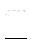
41309401th rev.4 49 / broadcast confirmation report 07/01/2000 17:05 id=oki pages = 01 start time = 07/01 10:00 total time = 00:02'30" location id pages result location id pages result one touch 1 = head office 01 ok 2 = ot2 01 ok 3 = ot3 01 ok 4 = ot4 01 ok 5 = ot5 01 ok auto dial 01 = ad1 01 ok 02...
Page 50: Power Outage Report
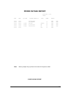
41309401th rev.4 50 / power outage report 07/01/2000 17:05 id=oki date time s,r-time distant station id mode pages result 06/30 10:10 0485-88-3385 lost 9080 06/30 10:30 ods takasaki 03 lost 0000 06/30 12:05 01'20" oki fax conf=01 03 lost 0000 06/30 13:00 00'20" 03-5476-4300 rx 01 lost 0000 06/30 10:...
Page 51: Confidential Rx Report
41309401th rev.4 51 / confidential rx report 07/01/2000 17:05 id=oki date time s,r-time distant station id mode pages result 07/01 17:00 00'00" oki fax conf=01 02 ok 0000 confidential rx report.
Page 52
41309401th rev.4 52 / call back message 07/01/2000 09:24 oki shibaura → oki honjo no.002 please call back oki shibaura ☎ 03 5476 1234.
Page 53
41309401th rev.4 53 / self diagnosis report print conditions 1) the following self diagnosis results are always printed. • cpu - rom, flash - program / language / default version read and hush check. • cpu-ram, flash - ram read/write check • image processor lsi ram check • setting default type and r...
Page 54
41309401th rev.4 54 / cpu-rom version aaaa hash ok hhhh cpu-ram ok program version aaaa hash ok hhhh language version aaaa hash ok hhhh default version aaaa hash ok hhhh ram1 4m ok *1 ram2 ok default type 01 03/03/2000 12:00 device id mfg:oki data corp; *2 mdl:fx-046fax; *2 des:oki fx-046fax; *2 opt...
Page 55
41309401th rev.4 55 / protocol dump the printing image is as follows: protocol dump p1 08/25/2000 19:00 id=oki takasaki data 04/19 time 14:49 s,r-time 00’07" distant station id oki shibaura(6412) mode tx-g4 pages 02 ok 0000 result tx setup conn-ack +bch+ disc rel-c rx tx sabm sq cr tcr css cdcl cds ...
Page 56
41309401th rev.4 56 / protocol dump p2 cr/cn 00 00 00 00 00 00 00 00 00 00 00 00 00 00 00 00 00 00 00 00 00 00 00 00 00 00 00 00 00 00 00 00 00 00 00 00 00 00 00 00 00 00 ca/cc 00 00 00 00 00 00 00 00 00 00 00 00 00 00 00 00 00 00 00 00 00 00 00 00 00 00 00 00 00 00 00 00 00 00 00 00 00 00 00 00 00 ...
Page 57
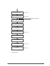
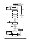
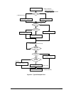
41309401th rev.4 57 / 2. Installation procedure 2.1 setup information 2.1.1 general the following flowchart outlines the installation procedure. Site selection (see 2.1.2) unpacking (see 2.1.3) check of contents (see 2.1.4) installation of attachments (see 2.1.5) ac cord connection (see 2.1.6) telep...
Page 58
41309401th rev.4 58 / dual access operations (see 2.2.1.7) system data programming (see 2.2.1.8) one-touch key programming two-digit auto dial programming group setting dial parameter settings (see 2.2.1.9) programming mail box password (see 2.2.1.10) on-line tests (see 2.2.1.11) 1 tsi/sender id inc...
Page 59
41309401th rev.4 59 / 2.1.2 site selection installation precautions for installation (1) fluctuation in line voltage • 120vac (102v to 127v) • 230vac (198v to 264v) (2) room temperature 50 to 90 ° f (10 to 32 ° c) (3) humidity 20 to 80% rh (4) operating environment pressure: equivalent to altitude o...
Page 60
41309401th rev.4 60 / note: 1 this space is necessary for having the telephone set. (page 62) 2 this space is necessary for installing the document stacker. 3 this space is necessary for ventilation. (7) levelness of installation surface 1 degree max. (8) other requirements avoid installing in any o...
Page 61
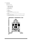
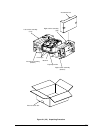
41309401th rev.4 61 / external carton box packing tape carton label packing tape figure 2.1 (1/2) unpacking procedure 2.1.3 unpacking procedure (1) remove tape on the top of the carton box and open its cover. (2) take out the accessory box from the carton box. (see figure 2.1) (3) take out the machi...
Page 62
41309401th rev.4 62 / figure 2.1 (2/2) unpacking procedure left cushion assembly (bottom) fixed tape machine front polyethylene film right cushion assembly (top) right cushion assembly (bottom) accessories box left cushion assembly (top) external carton box.
Page 63
41309401th rev.4 63 / item no. Name q'ty remarks 1 okifax4550/ 1 okioffice87 2 ac power cord 1 3 i/d unit 1 already installed. 4 toner cartridge 1 5 line cord 1 6 one touch sheet 1 already installed. 7 user's guide 1 vol. 8 tray paper 1 9 tray document 1 10 document stacker 1 table 2.1 contents list...
Page 64
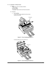
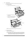
41309401th rev.4 64 / 2.1.5 installation of attachments (1) items • image drum (id) unit (already installed) • toner cartridge • recording paper • tray-paper, tray-document and document-stacker (2) procedure 1) toner cartridge • peel off the fixed tape attached to the cover-top. • open the cover-top...
Page 65
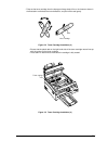
41309401th rev.4 65 / • take out the toner cartridge from the damp proof bag, shake it five or six times as shown in the illustration to eliminate the toner deflection, and peel off the seal gently. Figure 2.2 toner cartridge installation (3) • ensure that the plastic tab on the right-hand side of t...
Page 66
41309401th rev.4 66 / • push the gray tab forward until it stops. Figure 2.2 toner cartridge installation (5) • clean the toner scattered in the vicinity of the toner cartridge using a cloth moistened with cold water. Do not use hot water since it makes the toner stick there. • close the cover assem...
Page 67
41309401th rev.4 67 / (3) recording paper note: about 100 sheets of the new paper can be set on the tray-paper. Loading the new paper. Sheets must not exceed 100 sheets of the new paper on the tray-paper. If excessive sheets are set, it will cause paper jams. Figure 2.3 recording paper cassette inst...
Page 68
41309401th rev.4 68 / (4) tray-paper, tray-document and document-stacker • hang the tray-paper, the tray-document and the stacker-document onto hanging position. Figure 2.4 document stacker installation tray-paper tray-document cover-top stacker-document.
Page 69
41309401th rev.4 69 / 2.1.6 ac cord connection the power supply is provided as follows. Nominal input voltage 120vac (voltage range 102 to 127vac) nominal input voltage 230vac (voltage range 198 to 250vac) check whether the ac voltage of your input is within the above-mentioned voltage range and if ...
Page 70
41309401th rev.4 70 / 2.1.7 telephone and line connections (1) procedure • connect the lines. 2.1.8 packing for shipment caution: when packing the okifax4550/okioffice87 series for shipment, remove the image drum and toner from the unit and ship separately! Failure to do this will result in damage t...
Page 71
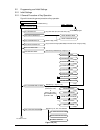
41309401th rev.4 71 / 2.2 programming and initial settings 2.2.1 initial settings 2.2.1.1 general procedure of key operation figure 2.6 shows the general procedure of key operation. (standby mode) select function (ot) ot1: delayed tx f (press the select function key.) [prg. Start date (0-9) and star...
Page 72
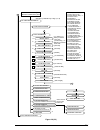
41309401th rev.4 72 / ot9: user programming powered on while holding the select function key down. Selection by yes/no keys or digit (1 to 8) 01: mcf. (signle-loc.) 02: mcf. (multi-loc.) 03: err. Report (mcf.) *4 04: image in mcf. 05: sender id 06: monitor volume 07: buzzer volume 08: closed network...
Page 73
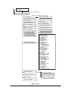
41309401th rev.4 73 / techinical programming powered on while holding the copy key down. Selection by yes/no keys or digit (1 to 5) selection by yes/no keys or digit (1 to 8) *5 *5 *5 *5 *5 *5 *5 *5 *5 selection by yes/no keys or digit (1 to 3) 01: service bit 02: monitor cont. 03: country code 04: ...
Page 74
41309401th rev.4 74 / note: when the machine is in power save mode, the machine returns to standby mode by pressing the start key. *1: in case of germany, austria and switzerland version, activity report message does not appear on the lcd display. *2: user can read no. Of counter in lcd but can not ...
Page 75
T.F. No. Item specifications default 41309401th rev.4 75 / 2.2.1.2 technical functions this section explains setting items generally conducted by service personnel, not by users. Table 2.2 shows the initial setting items and their purposes. (the default setting is different by the individual countri...
Page 76
T.F. No. Item specifications default 41309401th rev.4 76 / table 2.2 (1/8) service personnel initial settings 01 service bit 02 line monitor control 03 country code 04 time and date print 05 tsi print switching serviceman/user operation. On : service personnel’s features are available. Off : service...
Page 77
T.F. No. Item specifications default 41309401th rev.4 77 / table 2.2 (2/8) service personnel initial settings 06 tad mode (for external telephone answering device.) 07 real time dialing 08 tel/fax switching switches an automatic voice message response to the calling station. Tad mode is of three typ...
Page 78
T.F. No. Item specifications default 41309401th rev.4 78 / table 2.2 (3/8) service personnel initial settings echo protection ignore 1st dis ced-dis timer tone for echo off off 75 ms off on on 1.5 sec on (tf-11 table) 09 mdy/dmy 10 long document scan 11 tone for echo 12 mh only 13 high-speed modem r...
Page 79
T.F. No. Item specifications default 41309401th rev.4 79 / table 2.2 (4/8) service personnel initial settings 16 t2, timeout value 17 dis bit32 18 error criterion 19 off-hook bypass 20 nl equalizer 21 modem attenuator t2, timeout value (layer) registers the time duration (in seconds) for which the r...
Page 80
T.F. No. Item specifications default 41309401th rev.4 80 / table 2.2 (5/8) service personnel initial settings 0 to 15 db. Selectable (except fre) 7 to 15 db, selectable (fre) at country code = chn, set the actual set value +2db. Note: the send signal power level should meet your country’s regulation...
Page 81
T.F. No. Item specifications default 41309401th rev.4 81 / table 2.2 (6/8) service personnel initial settings 27 media type 28 transfer roller latch current 29 nsf switch selects the recording paper according to its quality. Medium, medium-heavy and heavy selectable. Selects the latch current for tr...
Page 82
T.F. No. Item specifications default 41309401th rev.4 82 / selects id/tsi printing in the distant station id column of the report. Id: prints nsf signal with personal id. Tsi: prints tsi signal without nsf. Note: lcd display and report printing gives preference to tsi/csi signal than per- sonal id. ...
Page 83
T.F. No. Item specifications default 41309401th rev.4 83 / set up whether to make fax2net service. On: enable off: disable * the following fax2net service can use only when fax2net function is set to on. Web retrieval/broadcasting/prepaid regis- tration adjusts read start position of various machine...
Page 84
41309401th rev.4 84 / table 2.3 (1/2) technical default setting 1 oda 2 lta 3 e-int 4 ger 5 e-fre 6 0-aus 7 0-nzl 8 0-sin 9 0-hng 10 l-ag 11 irl 12 den 13 swe no. Technical setting items setting selection 1 2 3 4 5 6 7 8 9 10 11 12 13 14 15 16 17 18 19 20 21 22 23 24 25 26 27 28 29 30 31 32 33 34 35...
Page 85
41309401th rev.4 85 / table 2.3 (2/2) technical default setting 14 nor 15 sui 16 aut 17 hol 18 ita 19 esp 20 chn (21) factory no. Technical setting items setting selection 1 2 3 4 5 6 7 8 9 10 11 12 13 14 15 16 17 18 19 20 21 22 23 24 25 26 27 28 29 30 31 32 33 34 35 36 37 38 39 40 41 42 43 on/off o...
Page 86
41309401th rev.4 86 / 1) tel/fax automatic switching this function is used for the purpose of tel/fax automatic switching as follows. (1) if the machine detects a call with a cng signal indicating an auto send facsimile call, it starts an automatic document receiving operation. (2) if machine detect...
Page 87
41309401th rev.4 87 / telephone call or manual transmission calling party called party (tel/fax mode) ringing ced nsf, csi, dis dcn cml"off" load document press start button manual transmission cml on 2.1 sec tel/fax automatic switch over time (20/35 sec) *2 *3 cng detection period 14:14 t/f indicat...
Page 88
41309401th rev.4 88 / telephone call or manual transmission calling party called party (tad) ringing ced nsf, csi, dis cml on 2.1s indication of lcd message from answer machine to record your message in answering machine dcn cml "off" *1 answering machine switches to fax cng detection period 14:14 t...
Page 89
41309401th rev.4 89 / telephone call or manual transmission calling party called party (tad) ringing cml on indication of lcd message from answer machine to record your message in answering machine cml "off" answering machine switches to fax 15s cng is not detect cng detection period 14:14 tad telep...
Page 90
41309401th rev.4 90 / the display shows: 2:technical function yes( ← ) no( → /1-6) ← ← operations: to bring the lcd up to the desired message press select function key once, copy key twice and "2"key. (in case of no message in memory) press key. * "enter 01 - 39" when g4 option is not installed. ← s...
Page 91
41309401th rev.4 91 / 14:14 fax ← function copy copy ← see table 2.4 the display shows: (standby) → press select function key. Press copy key twice. Press key. ← press key. → press key. ← operations: select function (ot) memory avail.=100% tech. Programming yes( ← /1-5) no( → ) 1:local test yes( ← )...
Page 92
41309401th rev.4 92 / table 2.4 (1/6) technial functions t.F. No. Name of function the display shows 01 service bit 02 line monitor control 03 country code 04 time and date print 05 tsi print 06 tad mode (for external telephone answering device.) 07 real-time dialling 08 tel/fax switching 01:service...
Page 93
41309401th rev.4 93 / table 2.4 (2/6) technial functions t.F. No. Name of function the display shows 11 tone for echo (echo protection) 12 mh only 13 high-speed modem rate 14 t1 (tx), timeout value (xtto value) 12:mh only [ x ] yes( ← ) no( → ) → setting (toggle) x: off on → ← 11:tone for echo [ x ]...
Page 94
41309401th rev.4 94 / table 2.4 (3/6) technial functions t.F. No. Name of function the display shows 17 dis bit 32 20 nl equalizer 21 modem attenuator 19 off-hook bypass 16 t2, timeout value 16:t2 timer *100ms [ x ] yes( ← ) no( → ) to 17: dis bit32 x: 001 - 255 → 16:t2 timer *100ms [ ] enter 001-25...
Page 95
41309401th rev.4 95 / table 2.4 (4/6) technial functions t.F. No. Name of function the display shows 23 mf attenuator 25 cml timing 26 led head strobe 23:mf att. [ x ] yes( ← ) no( → ) 26:led head strobe [ x ] yes( ← ) no( → ) → setting x:0 db → 1 db → 24:ring dura. *10 ms [ x ] yes( ← ) no( → ) to ...
Page 96
41309401th rev.4 96 / table 2.4 (5/6) technial functions t.F. No. Name of function the display shows media type 27 transfer roller clatch current 28:tr latch current [ x ] yes( ← ) no( → ) x: off on → ← → setting x:-2 -1 → 0 → +1 → +2 → 27:media type [ x ] yes( ← ) no( → ) → setting x: m mh → h → 29...
Page 97
41309401th rev.4 97 / table 2.4 (6/6) technial functions t.F. No. Name of function the display shows top feed 38 bottom feed 39:bottom feed [ x ] yes( ← ) no( → ) x: off on → ← → setting x:1 → 2 → 3 10 → -1 → -2 → -3 0 → -2 38:top feed [ x ] yes( ← ) no( → ) → setting x:1 → 2 → 3 9 → -1 → -2 → -3 -1...
Page 98
41309401th rev.4 98 / table 2.5 g3 fallback object service code list (if g4 tx is faulty) unallocated (unassigned) number no route to specified transit network no route to destination channel unacceptable call awarded and being delivered in an established channel procedure sequence error, line disco...
Page 99
41309401th rev.4 99 / 2.2.1.4 user’s functions this section explains the items usually set up by general users. Table 2.6 shows the initial setting items and their purposes. Each f.P.Can be accessed by entering the corresponding function number on function program- ming. The detailed procedure of th...
Page 100
41309401th rev.4 100 / table 2.6 (1/7) user's functions no. Item specifications 1) user's functions 1 auto dial 1) one-touch dial 10 one-touch keys are provided. (okifax4550/ okioffice87) max. 32 digits for each location number for okifax4550. Max. 40 digits for each location number for okioffice87....
Page 101
41309401th rev.4 101 / no. Item specifications table 2.6 (2/7) user's functions 3: when web url is registered in a one-touch in a group, the one-touch is deleted from the group destination. 4: since the okifax4550 and okioffice87 are already registered in web url, the registered contents are stored ...
Page 102
41309401th rev.4 102 / table 2.6 (3/7) user's functions no. Item specifications 3) keypad dial 4) chain dial 5) mixed dial 2 manual dial 3 receive mode 1) auto receive mode 2) manual recevice mode 3) telephone/fax automatic switchover max. 32 digits for each location number for okioffice87. Max. 40 ...
Page 103
41309401th rev.4 103 / 4 automatic redial 5 last no. Redial 6 group dial 7 telephone directory and location id (alpha search) table 2.6 (4/7) user's functions no. Item specifications ptt parameter setting disables or enables this feature, and specifies redial times and redial intervals. * see 2.9.9 ...
Page 104
41309401th rev.4 104 / no. Item specifications table 2.6 (5/7) user's functions 8 local copy 9 multiple local copy 10 manual loading feeder 11 broadcast (memory transmission) 12 delayed transmission from the memory 13 polling transmission (to be polled) 14 polling reception 15 bulletin polling 16 tr...
Page 105
41309401th rev.4 105 / table 2.6 (6/7) user's functions no. Item specifications the fax can temporarily store received messages in memory when toner has run out. The messages are printed when toner has been newly supplied or an operator presses the select function key followed by the one-touch key n...
Page 106
41309401th rev.4 106 / table 2.6 (7/7) user's functions no. Item specifications dual access combination table reception prefeed remote input display preparation tx scanning to memory standby during fax calling during ring response during detection of tel/fax during tad detection 1st phase b calling ...
Page 107
41309401th rev.4 107 / 2) user's initial settings note: the fonts displayed on the lcd operation panel may differ from fonts written this manual. 2)-1 one touch key operations 1 4 : 1 4 f a x e n t e r i d → [ x x x x ] 1 4 : 1 4 f a x 0 7 / 0 1 / 2 0 0 0 1 4 : 1 4 f a x s e l e c t l o c a t i o n ...
Page 108
41309401th rev.4 108 / table 2.7 (1/6) user's initial settings (one-touch key program) f+ot item specifications no. 1 delayed transmission (tx) 2 print from message in memory (print memory msg.) print from confidential reception message (print personal box) 3 confidential transmission 4 relay broadc...
Page 109
41309401th rev.4 109 / table 2.7 (2/6) user's initial settings (one-touch key program) f+ot item specifications no. The report print in 6 items are as follows: 1. Activity report 2. Broadcast message confirmation report (multi location) 3. Activity memory files report 4. Phone directory report 5. Co...
Page 110
41309401th rev.4 110 / 8 location program 1. One-touch key 2. Two-digit or max. Three-digit auto dial program 3. Group setting 9 user’s programs 1. Function program table 2.7 (3/6) user's initial settings (one-touch key program) f+ot item specifications no. One-touch keys allow registering: (1) tele...
Page 111
41309401th rev.4 111 / table 2.7 (4/6) user's initial settings (one-touch key program) f+ot item specifications no. 2. Dial parameters 3. Clock adjustment 4. System data program 5. Personal box programming 6. Forwarding number program- ming 1. Redial tries 2. Redial interval 3. Dial tone detect 4. B...
Page 112
41309401th rev.4 112 / table 2.7 (5/6) user's initial settings (one-touch key program) f+ot item specifications no. 7. Memory password programming 8. Fax network programming 9. Fax2net service 10. Restrict id programming registering the password required (4-digit numerals) for outputting the data re...
Page 113
41309401th rev.4 113 / table 2.7 (5/6) user's initial settings (one-touch key program) f+ot item specifications no. 11. Isdn programming 10 printer cleaning sets to country code, isdn no. (subscriber number), isdn id (subscriber code) and isdn sub address. 1) setting values this setting consists of ...
Page 114
41309401th rev.4 114 / p.F. Item specifications default no. Table 2.8 (1/6) user's initial settings (function program) 2)-2 function program 01 message confirmation report (single location) 02 message confirmation report (multiple locations) 03 error report (mcf) 04 image in mcf 05 sender id 06 moni...
Page 115
41309401th rev.4 115 / p.F. Item specifications default no. Table 2.8 (2/6) user's initial settings (function program) the fax compares lower four digits of tsi/csi received from remote station with fax numbers registered locally for one-touch dial and two-digits autodial. If unmatched, the communic...
Page 116
41309401th rev.4 116 / 14 user language 15 incoming ring 16 remote receive 17 memory and feeder switch 18 power save mode 19 ecm function 20 remote diagnosis table 2.8 (3/6) user's initial settings (function program) p.F. Item specifications default no. A choice of 2 languages for lcd and print mes-...
Page 117
41309401th rev.4 117 / table 2.8 (4/6) user's initial settings (function program) p.F. Item specifications default no. To enable or disable pc interface function. When pc reception is not available, for example, application is not activated on the pc or cable is missing between pc and fax etc., this...
Page 118
41309401th rev.4 118 / std 97.9% 94.5% a4 size except a4 size fine 97.5% 95.0% 8 dot/mm 94.1% 300 dpi 92.6% ex fine 97.5% 95.0% table 2.8 (5/6) user's initial settings (function program) p.F. Item specifications default no. This function can print characters written at the edges of a document. Switc...
Page 119
41309401th rev.4 119 / table 2.8 (6/6) user's initial settings (function program) p.F. Item specifications default no. Determine whether the incoming call is answered when the information transmission capacity instracted by the network is voice transmission. 1) setting values on(answered)/off(not an...
Page 120
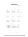
41309401th rev.4 120 / table 2.9 (1/2) user default setting 1 2 3 4 5 6 7 8 9 10 11 12 13 14 15 16 17 18 19 20 21 22 23 24 25 26 27 28 29 30 31 32 33 34 mcf (single-loc.) mcf (multi-loc.) err.Report (mcf.) image in mcf. Sender id monitor volume buzzer volume closed network tx mode default t/f timer ...
Page 121
41309401th rev.4 121 / table 2.9 (2/2) user default setting 1 2 3 4 5 6 7 8 9 10 11 12 13 14 15 16 17 18 19 20 21 22 23 24 25 26 27 28 29 30 31 32 33 34 mcf (single-loc.) mcf (multi-loc.) err.Report (mcf.) image in mcf. Sender id monitor volume buzzer volume closed network tx mode default t/f timer ...
Page 122
41309401th rev.4 122 / the display shows: 1:func. Programming yes( ← ) no( → /1-9*#) to an individual setting item. (see table 2.10) ← operations: press key. ← enter two-digit function number, then the display will show the set item corresponding to the number entered. If you want to set up all or s...
Page 123
41309401th rev.4 123 / table 2.10 (1/4) user's functions 01:mcf(single-loc.) [ x ] yes( ← ) no( → ) tap no. Name of function the display shows 0 1 message confirmation report (single location) message confirmation report (multiple locations) error report sender id monitor volume closed network buzze...
Page 124
41309401th rev.4 124 / table 2.10 (2/4) user's functions 13:paper size [ x ] yes( ← ) no( → ) tap no. Name of function the display shows 1 3 paper size remote receive → setting note 3 incoming ring 15:incoming ring [ x ] yes( ← ) no( → ) → setting x: mem. Feed. 1 4 1 5 1 6 off 00 11 22 33 44 55 77 8...
Page 125
41309401th rev.4 125 / table 2.10 (3/4) user's functions 22:no toner mem. Rx [ x ] yes( ← ) no( → ) tap no. Name of function the display shows 2 2 no toner memory reception restricted access 23:mem full save [ x ] yes( ← ) no( → ) → setting (toggle) → setting (toggle) instant dialing 25:instant dial...
Page 126
41309401th rev.4 126 / table 2.10 (4/4) user's functions 31:speech receive [ x ] yes( ← ) no( → ) tap no. Name of function the display shows 3 1 speech receive 32:usb conv. Mode [ x ] yes( ← ) no( → ) → setting (toggle) → setting (toggle) print job time out 35:print job t.O. [ x ] yes( ← ) no( → ) 3...
Page 127
41309401th rev.4 127 / note 1: resolution & original of tx mode defult setting can be selected by using → key. 2: when the service bit is set to "off" and the corresponding bit of xpara of national code is set to "off", ring response and/or distinctive ring is bypassesd as follows: std / normal std ...
Page 128
41309401th rev.4 128 / operations: (each ring response time of 5,10,15 or 20 sec. Is given by pressing key.) 11 entered. Select function (ot) memory avail.=100% ← ← x: 1ring → 05sec → 10sec 20sec ← 15sec ← ← → → to bring the lcd up to the desired message, press select function key once and one-touch...
Page 129
41309401th rev.4 129 / 2:dial parameter yes( ← ) no( → /1-9*#) ← redial interval [1 min] yes( ← ) no( → ) ← → dial tone detect [ on ] yes( ← ) no( → ) ← → busy tone detect [ on ] yes( ← ) no( → ) ← mf(tone)/dp(pulse) [ m f ] yes( ← ) no( → ) ← → dial prefix [ off ] yes( ← ) no( → ) ← flash/earth/nor...
Page 130
41309401th rev.4 130 / table 2.11 dial parameters setting if the service bit "off" note: the blank in the table is not indicated on the lcd. National code usa int'l gbr irl nor swe fin den ger hun tch pol redial tries redial interval busy tone detect mf/dp pulse dial rate pulse make ratio pulse dial...
Page 131
41309401th rev.4 131 / operations: 3 select function (ot) memory avail.=100% 1:func. Programming yes( ← ) no( → /1-9) 3:clock adjustment yes( ← ) no( → /1-9*#) [07/01/2000 14:14] yes( ← ) no( → /0-9) ← key to bring the lcd up to the desired message, press select function key once and one-touch key n...
Page 132
41309401th rev.4 132 / oki tokyo sending /144 oki tokyo receiving/144 oki tokyo memory-rx/144 set documents during memory tx or set documents during feeder tx after the end of the pre-scanning set documents set documents select location oki takasaki yes(start) no(loc.) select function (ot) memory av...
Page 133
41309401th rev.4 133 / note 1: use the unique key to input special symbols. 2: when 16 digits or more is registered, the high-order 16 digits are displayed (tsi, csi, id or cbm) operations: select function (ot) memory avail.=100% 1:func. Programming yes( ← ) no( → /1-9*#) 4:system data prg. Yes( ← )...
Page 134
41309401th rev.4 134 / operations: the display shows: press key. No=03 3404 7123 id=oki no= no=_ no=03 3404 7765_ 1 03......5 (example) start continued from the previous page. (example) 3 sec later start start press key. Start.
Page 135
41309401th rev.4 135 / operations: select function (ot) memory avail.=100% to bring the lcd up to the desired message, press select function key once and one-touch key no. 9 in the standby mode. (in case of no message in memory) the display shows: press key. ← 1:func. Programming yes( ← ) no( → /1-9...
Page 136
41309401th rev.4 136 / the display shows: 2:dial parameter yes( ← ) no( → /1-9*#) ← → ← → ← → ← → ← → ← → pulse make ratio [ 33% ] yes( ← ) no( → ) ← → ← → ← → ← → ← ← → ← ← (1) redial time "0 try" to "10 try", "1 try" to "5 try" (country code=fre) (2) redial interval "1 min" to "6 min", "1 min" to ...
Page 137
41309401th rev.4 137 / table 2.12 default settings of dial parameters 24 sin no. User setting items setting selection note: user settings are possible for items without mesh. Redial tries redial interval dial tone detect busy tone detect mf (tone)/dp (pulse) pulse dial rate pulse make ratio pulse di...
Page 138
41309401th rev.4 138 / table 2.13 dial parameters settings no. Item specifications dial parameters 01 redial tries 02 redial interval 03 dial tone detect 04 busy tone detect 05 mf (tone) or dp (pulse) 06 pulse dial rate 07 pulse make ratio 08 pulse dial type 09 mf (tone) duration 10 pbx line 11 flas...
Page 139
41309401th rev.4 139 / operations: tech. Programming yes( ← /1-5) no( → ) to bring the lcd up to the desired message, press select function key once and copy key twice in the standby mode. (in case of no message in memory) the display shows: press key. ← 1: local test yes( ← ) no( → /1-5) ← 1: self ...
Page 140
41309401th rev.4 140 / figure 2.7 printed data of self-diagnosis print test (example) cpu-rom version aaaa hash ok hhhh cpu-ram ok program version aaaa hash ok hhhh language version aaaa hash ok hhhh default version aaaa hash ok hhhh ram1 4m ok *1 ram2 ok default type 01 03/03/2000 12:00 device id m...
Page 141
41309401th rev.4 141 / 2.2.1.11 on-line tests 1. Transmission (1) load documents (2) make sure that • the loaded documents are fed in automatically. • the std and normal lamps light. • the display shows select location. (3) dial the telephone number of the remote machine by the ten-key pad. (4) make...
Page 142
41309401th rev.4 142 / figure 2.8 typical transmission flow x x : x x x x x (standby condition) auto dialing? Which mode? Yes no one-touch • one-touch key (e.G. No. 1) two-digit auto dial code • press "auto dial" key • set the code (e.G. 01) (• load document(s), select resolution mode) ced received?...
Page 143
41309401th rev.4 143 / figure 2.9 typical reception flow x x : x x x x x auto receive mode? Yes no manual receive mode 3 3 4 5 4 2 1 1 1 r e c e i v i n g / 1 4 4 o k i t a k a s a k i r e c e i v i n g / 1 4 4 message reception completed? Received dcn? No yes local problem occurred? R e s u l t = o...
Page 144
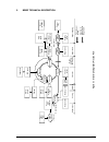
41309401th rev.4 144 / figure 3.1 electro-photographic process flow 3. Brief technical description pwu board charger cleaning roller pwu board paper path selector heater roller fusing back-up roller image data led head developing roller doctor blade toner supply roller pwu board toner cartridge tran...
Page 145
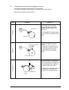
41309401th rev.4 145 / process illustration description the surface of the electro-photo- graphic image drum is uniformly charged with negative charges by applying a negative voltage to the charge roller. When the applied dc voltage exceeds a threshold value, charging of the drum begins. Light emitt...
Page 146
41309401th rev.4 146 / process illustration description ep drum transfer roller paper power supply power supply cleaning roller ep drum transfer roller back-up roller paper heater roller heater transfer 4 cleaning 6 fusing 5 the recording paper is placed over the image drum surface and a positive ch...
Page 147
41309401th rev.4 147 / figure 3.2 actual ep process 5 heater roller 6 cleaning roller 1 charge roller 2 led head back-up roller 4 transfer roller recording paper 3 developing roller electro-photographic drum toner * process: 1 : charging 2 : exposure 3 : developing 4 : transfer 5 : fusing 6 : cleani...
Page 148
41309401th rev.4 148 / 3.3 boards and units 3.3.1 boards and units the following one board, main control board and three units constitute the facsimile transceiver machine. • main control board mcnt: (46f: okifax4550, r46: okioffice87) • network control unit board ncu: (inu/en9) • operation panel as...
Page 149
41309401th rev.4 149 / ac inlet ncu or g4 sub main p2h ope (04w) led head d motor clutch fuser s motor pc1 pc2 cis speaker prt scan cn1 cn cn2 cn cn3 cn7 cn6 cn1 cn1 cn5 cn4 cn3 cn cn cn cn2 cn1 cn cn cn13 cn (r46 only) cn14 cn12 cn2 cn1 cn3 cn cn cn9 cn cn10 cn1 cn2 cn3 cn cn cn cn cn cn cn mpw1446...
Page 150
41309401th rev.4 150 / 3.4 overall dimension and mechanical structure of okifax4550/okioffice87 figure 3.4 overall dimension and mechanical structure document paper ep drum roller - heater paper exit id unit led head scanner block roller - adf separation rubber ope board roller - scan document exit ...
Page 151
41309401th rev.4 151 / 4. Mechanical disassembly and reassembly general the section explains the procedures for replacement of parts, assemblies, and units in the field. Only the disassembly procedures are explained here. For reassembly, reverse the disassembly procedure. 4.1 precautions for parts r...
Page 152
41309401th rev.4 152 / id unit cover assembly-top caution: do not expose the i/d unit to direct sunlight. To protect the i/d unit against room lights, cover it with a4-size paper or the like. Board or part adjustment (a) ncu board dip switches to be placed in the same position as on the removed boar...
Page 153
41309401th rev.4 153 / table 4.1 tools no. Service tools philips screw driver (l) q'ty remarks philips screw driver (m) flat screw drivers (s) philips screw driver (s) radio pliers nippers multimeter 1 2 3 4 5 6 7 1 1 1 1 1 1 1 short-ciucuit test 4.2 tools table 4.1 shows the tools required for the ...
Page 154
41309401th rev.4 154 / figure 4.1 (1/2) disassembly procedure flow start open the cover assembly-top (4.3.1) open the frame assembly scanner (u) (4.3.4) led print head (4.3.1) cap-tel-i/f (4.3.2) separation rubber (4.3.4) open the ope panel assembly (4.3.3) bracket-package (4.3.3) board (4.3.6) prin...
Page 155
41309401th rev.4 155 / figure 4.1 (2/2) disassembly procedure flow open the ope panel assembly heat assembly (4.3.14) plessure roller b (backup roller) (4.3.15) paper sensor e paper sensor exit toner sensor assy. (4.3.17) plate-side m gear-idle (4.3.11) + hopping shaft assy. (4.3.16) separation plat...
Page 156
41309401th rev.4 156 / figure 4.2 appearance of the okifax4550/okioffice87.
Page 157
41309401th rev.4 157 / cover assembly-top led head pc connector 4.3.1 led print head it is used two kind of head as the led print head. (208 mm width or 216 mm width) (1) disassembly procedure a) open the cover assembly-top by raising. Note: be sure not to touch directly or push the sla part of the ...
Page 158
41309401th rev.4 158 / id unit cover assembly-top fixing hook cover-rear screw 1 4.3.2 id unit, rear-cover, cover-main, board-ncu or board-g4n (1) disassembly procedure a) open the cover assembly-top by raising. B) take out the id unit from the equipment. C) cover-rear: remove the cover-rear by remo...
Page 159
41309401th rev.4 159 / holder assembly guide-paper (l) guide-paper (r) cover-main board-ncu or board-g4n or screw 3 d) board-ncu and board-g4n remove the board-ncu or board-g4n by removing the two screw 3 and disconnect the connector (cn3) from board-46f or r46. E) first, move the center of guide-pa...
Page 160
41309401th rev.4 160 / cable 2 ope panel assembly screw 3 fixing hook screw 4 lcd (1) disassembly procedure a) first, carry out the disassembly pro- cedure up to the point of the 4.3.2 (item (e). Cover-main). B) dismount the printer-unit. (see section 4.3.18) c) open the ope-panel assembly. D) ope p...
Page 161
41309401th rev.4 161 / frame assembly-scanner (u) gear (z31) bearing s a roller assembly sensor spring (l) red mark view from a spring (r) earth cable plate-support 4.3.4 separation rubber, roller assembly sensor (1) disassembly procedure a) separation rubber: the separation rubber can be removed fr...
Page 162
41309401th rev.4 162 / screw 1 screw 1 frame assembly-scanner 4.3.5 roller assembly-adf, cis (contact image sensor), lever-pc1 and pc2 (1) disassembly procedure a) first, carry out the disassembly procedure up to the point of the 4.3.2 and 4.3.3. B) dismount the printer-unit. (see section 4.3.18) c)...
Page 163
41309401th rev.4 163 / plate scanner (l) plate scanner (r) plate scanner b plate earth adf roller assembly-adf speaker cis lever pc2 lever pc1 roller assy-adf d) turn the frame assembly-scanner in- side out and perform the disassembly procedure. E) remove the plate scanner (l) by re- moving the two ...
Page 164
41309401th rev.4 164 / screw 1 motor-s connector pc2 pc1 plate scanner b j) motor-s: remove the motor-s by removing the connector of motor and the two screws 1 . K) photo-sensor (pc1, pc2): after disconnecting the two connec- tors, remove the photo-coupler sen- sors pc1 and pc2 on the plate scan- ne...
Page 165
41309401th rev.4 165 / 4.3.6 board-46f, board-r46 power supply unit, board hv-p6l (1) disassembly procedure a) first, carry out the disassembly procedure up to the point of the 4.3.2 (cover-rear, cover-main etc.). B) board-46f or r46: disconnect the all connectors. C) remove the board-46f or r46 by ...
Page 166
41309401th rev.4 166 / led head flat cable assy heat assy pressure roller (b) (back up roller) transfer roller paper guide (r) papr guide (l) hopper spring resistration roller drive shaft e (eject) idle gear heat side plate m tension plate hopping shaft assy magnet h (hopping shaft) roller holder ho...
Page 167
41309401th rev.4 167 / registration bearing transfer roller registration bearing gear t label 4.3.8 transfer roller (1) disassembly procedure a) open the cover assembly-top by rais- ing and remove the id unit. B) remove the right claw. Then, dismount transfer roller, two registration bearing, and ge...
Page 168
41309401th rev.4 168 / cable 3 screw 1 screw 1 tlhv/olhv board cable 4 4.3.9 high-voltage power supply unit (hv-p2h) (1) disassembly procedure a) first, carry out procedure up to the point of the 4.3.2 (id unit, cover-rear and cover-main). B) remove three screws 1 then remove cover- hv and draw out ...
Page 169
41309401th rev.4 169 / guide-paper (l) guide-paper (r) spring-holder spring-stopper holder-paper bracket-package 4.3.10 holder assembly (1) disassembly procedure a) first, carry out procedure up to the point of the 4.3.2 (id unit, cover- rear and cover-main). B) dismount the bracket-package. C) dism...
Page 170
41309401th rev.4 170 / screw 1 gear r idle gear 2r earth plate idle gear m idle gear p idle gear 3p plate side-m idle gear p idle gear heat idle gear r a) first, carry out procedure up to the point of the 4.3.2 (id unit, cover- rear and cover-main). B) remove two screws 1 and two claws, then dismoun...
Page 171
41309401th rev.4 171 / registration roller registration bearing 4.3.12 registration roller (1) disassembly procedure a) first, carry out procedure up to the point of the 4.3.2 (id unit, cover- rear and cover-main). B) move registration roller to the right and dismount it by lifting. (two regis- trat...
Page 172
41309401th rev.4 172 / screw 1 eject roller screw 1 idle gear e (b) idle gear e (a) drive shaft e (eject) 4.3.13 drive shaft e (eject) and eject roller (1) disassembly procedure a) first, carry out procedure up to the point of the 4.3.2 (id unit, cover-rear and cover-main). B) remove two screws 1 fr...
Page 173
41309401th rev.4 173 / screw 1 connector 2 heat assembly screw 1 halogen lamp voltage display side left heat bearing right heat bearing heat gear heat roller thermostat heat contact heat code thermister screw 3 terminal plate 4.3.14 heat assembly this section explains how to dismount the heat assemb...
Page 174
41309401th rev.4 174 / pressure roller b bearing bu bearing bu bias spring bias spring 4.3.15 pressure roller b (back up roller) (1) disassembly procedure a) first, carry out procedure up to the point of the 4.3.2 (id unit, cover-rear and cover-main). B) dismount the high-voltage power sup- ply boar...
Page 175
41309401th rev.4 175 / hopping roller roller holder magnet h hopping shaft assembly knock pin 4.3.16 hopping shaft assembly (1) disassembly procedure a) first, carry out procedure up to the point of the 4.3.2 (id unit, cover-rear and cover-main). B) dismount the high-voltage power sup- ply board. (s...
Page 176
41309401th rev.4 176 / paper sensor exit toner sensor assembly paper sensor e 4.3.17 paper sensor e, paper sensor exit and toner sensor assembly (1) disassembly procedure a) first, carry out procedure up to the point of the 4.3.2 (id unit, cover-rear and cover-main). B) dismount the high-voltage pow...
Page 177
41309401th rev.4 177 / 4.3.18 printer unit (1) disassembly procedure a) first, carry out procedure up to the point of the 4.3.2 (id unit, cover-rear and cover- main). B) remove bracket-package with three screws, then disconnect cable-flat from connector on 46f or r46-board (m-cnt). C) pull out the h...
Page 178
41309401th rev.4 178 / 5. Adjustments 5.1 setting of led print head drive time • adjustment point: technical function no. 26. * to bring the lcd up to technical function, press select function key once, copy key twice and "2" key (in case of no message in memory). Note: when the rank marking of the ...
Page 179
41309401th rev.4 179 / 5.2.1 confirmation items the clock frequency and power voltage of the machine are not possible to adjust in the field. However, their measurement procedures are described here for confirmation of clock frequency and each voltage. 1) clock frequency • measurement point: 46f boa...
Page 180
41309401th rev.4 180 / 5.2.2 measurement 1) trun the ac power off. 2) carry out the disassembly procedure up to cover assembly-top, frame assembly-scanner, and unit-printer. (refer to the mechanical disassembly and reassembly in chapter 4.) 3) connect extension cables to the 46f board. 4) connect th...
Page 181
41309401th rev.4 181 / figure 5.2 measurement points on r46 board ground terminal ground terminal connector cn7 cn7-1 (+24vdc) cn7-2,3 (+5vdc) cn7-8 (+30vdc) cn7-9 (-8vdc) cn7-12 (+5vsub) ic24-9pin connector cn5-1 (sig) crystal oscillator.
Page 182
41309401th rev.4 182 / 6. Cleaning and maintenance 6.1 replacement of consumable the user (or service personnel) is required to replace the following items as consumable parts. (1) user side (2) service personnel side figure 6.1 consumable parts 1 toner cartrige 2 i/d unit (image drum unit) expected...
Page 183
41309401th rev.4 183 / table 6.1 reliability jam occurrence and misfeeds in the automatic document feeder will be less than one in 500 operations for all specified documents. Jam occurrence in the automatic paper feeder will be less than one in 1,500 operations and misfeeds will be less than one in ...
Page 184
41309401th rev.4 184 / 1 roller-scan 2 roller-adf 3 contact image sensor 4 separation rubber 5 led print head 6 printer unit 7 lubrication 8 cleaning clean with wet cloth. Clean with wet cloth. If the surface of this roller becomes dirty and the dirt causes misfeeding of documents, perform this clea...
Page 185
41309401th rev.4 185 / figure 6.2 parts of routine inspection document paper paper exit id unit (5) led head (2) roller - adf (4) separation rubber (1) roller - scan document exit (3) image sensor (6) printer block.
Page 186
41309401th rev.4 186 / the display shows: select function (ot) memory avail.= 100% drum count clear ( ← ) next( → ) are you sure ? Yes ( ← ) no( → ) print count xxxxxx next( → ) scan count xxxxxx next( → ) clear operations: to bring the lcd up to the desired message, press select function key once a...
Page 187
41309401th rev.4 187 / 1 4 : 1 4 f a x s e l e c t f u n c t i o n ( o t ) m e m o r y a v a i l . = 1 0 0 % → key ← key ← key ← key press function key. D r u m c o u n t c l e a r ( ← ) n e x t ( → ) a r e y o u s u r e ? Y e s ( ← ) n o ( → ) p r i n t c o u n t x x x x x x n e x t ( → ) s c a n c...
Page 188
41309401th rev.4 188 / note: drum (t) will be used to know the total in-use life of the machine. 6.4 printer counter display/clear 1. Purpose the service personnel can clear and check the following data: • image drum • toner • image drum (total) • print • scan 2. Procedure the following shows the ca...
Page 189
41309401th rev.4 189 / 1 : l o c a l t e s t y e s ( ← ) n o ( → / 1 - 5 ) 1 : s e l f d i a g n o s i s y e s ( ← ) n o ( → / 1 - 8 ) ← key ← key 1-8 1 2 3 → key or 1-5 → key technical programming self diagnosis ← key lt-9 lt-1 lt-3 4 5 lt-5 sensor calibration led test tone send test modem send tes...
Page 190
41309401th rev.4 190 / 6.5.2 when g4 option baord is installed. • when g4 option board is installed, the following items can be selected. Loop back 1 to pulse (n2khz) send • these tests are continued till stop key is pressed. 1 : l o c a l t e s t y e s ( ← ) n o ( → / 1 - 6 ) 1 : s e l f d i a g n ...
Page 191
41309401th rev.4 191 / 6.6 self-diagnosis test 1. Purpose to check roms, rams and printing function. 2. Procedure the display shows: ← operations: to bring the lcd up to the desired message, press select function key once and copy key twice in the standby mode. (in case of no message in the memory) ...
Page 192
41309401th rev.4 192 / 6.6.1 self diagnosis report 6.6.1.1 print conditions 1) the following self diagnosis results are always printed. • cpu - rom, flash - program / language / default version read and hush check. • cpu-ram, flash - ram read/write check • image processor lsi ram check • setting def...
Page 193
41309401th rev.4 193 / figure 6.3 self-diagnosis data cpu-rom version aaaa hash ok hhhh cpu-ram ok program version aaaa hash ok hhhh language version aaaa hash ok hhhh default version aaaa hash ok hhhh ram1 4m ok *1 ram2 ok default type 01 03/03/2000 12:00 device id mfg:oki data corp; *2 mdl:fx-046f...
Page 194
41309401th rev.4 194 / 6.7 sensor calibration test 1. Purpose to adjust the linearity of output levels of contact image sensor. The display shows: tech. Programming yes( ← /1-5) no( → ) ← operations: to bring the lcd up to the desired message, press select function key once and copy key twice in the...
Page 195
41309401th rev.4 195 / the display shows: ← operations: continued from the previous page ok load document(s). For adjustment of levels, use white plain bond paper(s) of na letter or a4 size. Press key. ← observe and check the document feed operation. Check that the followings do not occur: document ...
Page 196
41309401th rev.4 196 / 6.8 leds test 1. Purpose to check all leds on operation panel by lighting. 2. Procedure the display shows: ← operations: to bring the lcd up to the desired message, press select function key once and copy key twice in the standby mode. (in case of no message in memory) press k...
Page 197
41309401th rev.4 197 / 6.9 tone send test 1. Purpose to send the g3 tonal frequencies to the line. 2. Procedure the display shows: operations: to bring the lcd up to the desired message, press select function key once, copy key twice and key twice. (in case of no message in memory) 1:self diagnosis ...
Page 198
41309401th rev.4 198 / 6.10 high-speed modem send test 1. Purpose to check the telephone line quality in combination with a remote station programmed to the high-speed modem receive test mode. 2. Procedure the display shows: operations: to bring the lcd up to the desired message, press select functi...
Page 199
41309401th rev.4 199 / figure 6.4 high-speed modem send and receive test 6:modem rec. Test rx/ / ' "xxxx press key. Cml relay operates. ← 5:modem send test yes( ← ) no( → /1-8) 5:modem send test tx/ / ' " the display shows: : modem rate (e.G. 9.6k means 9600 bps) test time (minute, second) press sto...
Page 200
41309401th rev.4 200 / 6.11 high-speed modem receive test 1. Purpose to check the telephone line quality in combination with a remote station programmed to the high-speed modem send test mode. 2. Procedure the display shows: operations: to bring the lcd up to the desired message, press select functi...
Page 201
41309401th rev.4 201 / 6.12 mf send test 1. Purpose to send the multi-frequencies of tone dialling to the line. 2. Procedure the display shows: operations: to bring the lcd up to the desired message, press select function key once, copy key twice and key twice. (in case of no message in memory) 1:se...
Page 202
41309401th rev.4 202 / the display shows: operations: to bring the lcd up to the desired message, press select function key once, copy key twice and key twice. (in case of no message in memory) 1:self diagnosis yes( ← ) no( → /1-8) 8 8:tone(tel/fax) test yes( ← ) no( → /1-8) 8:tone(tel/fax) test ton...
Page 203
41309401th rev.4 203 / the display shows: operations: press select function key, provided that the service bit is on. 14:14 fax (standby) select function (ot) memory avail.=100% press one-touch key no.6 (printing) 1:activity report yes( ← ) no( → /1-6) 6:protocol dump yes( ← ) no( → /1-6) ← protocol...
Page 204
41309401th rev.4 204 / 6.14.1 g3 protocol dump purpose: to allow the serviceman to obtain a list of protocol signals transferred between the transmitter and receiver. Print conditions: • modem trace information for each tx/rx is printed. (informeation for rx is added on 2nd page.) • modem result cod...
Page 205
41309401th rev.4 205 / protocol dump p1 12/24/1998 19:00 id=oki takasaki date time s,r-time distant station id mode pages result 12/24 18:56 00'33" 123456789012345678901234 tx 002 ok 0000 fcf tx nss pps_mps pps_eop dcn rx nsf dis cfr mcf mcf tx rx tx rx tx rx transmitted frame dis 00 00 00 00 00 00 ...
Page 206
41309401th rev.4 206 / protocol dump p2 12/24/1998 19:00 id=oki takasaki received frame dis ff c8 01 00 73 17 22 00 00 00 00 00 00 00 00 00 00 00 00 00 dtc 00 00 00 00 00 00 00 00 00 00 00 00 00 00 00 00 00 00 00 00 dcs 00 00 00 00 00 00 00 00 00 00 00 00 00 00 00 00 00 00 00 00 nsf ff c0 04 00 00 8...
Page 207
41309401th rev.4 207 / ced nsf csi dis (04) (02) (01) rx (receiver) ringing signal tx (transmitter) dialling tsi nss (c2) (c4) training tcf cfr (21) training fax msg. Rtc pps•eop (fd,f4) mcf (31) dcn (df) : preamble 6.14.2 analysis from the data the printed out data permits to analyze g3 facsimile c...
Page 208
41309401th rev.4 208 / 6.14.3 fcf (facsimile control field) conversion table table 6.2 shows all fcf signals which are needed to analyze the printed out protocol dump data. Some signals have two different hexadecimal codes in accordance with the calling party or called party. Table 6.2 fcf signals c...
Page 209
41309401th rev.4 209 / 6.14.4 g4 protocol dump purpose: to allow the serviceman to obtain a list of protocol signals transmitter and receiver. Method: the report will be manually printed out for maintenance purpose. If it is g4, the g4 communication protocol dump is printed out. 1. Title of the repo...
Page 210
41309401th rev.4 210 / protocol dump the printing image is as follows: protocol dump p1 08/25/2000 19:00 id=oki takasaki data 04/19 time 14:49 s,r-time 00’07" distant station id oki shibaura(6412) mode tx-g4 pages 02 ok 0000 result tx setup conn-ack +bch+ disc rel-c rx tx sabm sq cr tcr css cdcl cds...
Page 211
41309401th rev.4 211 / protocol dump p2 cr/cn 00 00 00 00 00 00 00 00 00 00 00 00 00 00 00 00 00 00 00 00 00 00 00 00 00 00 00 00 00 00 00 00 00 00 00 00 00 00 00 00 00 00 ca/cc 00 00 00 00 00 00 00 00 00 00 00 00 00 00 00 00 00 00 00 00 00 00 00 00 00 00 00 00 00 00 00 00 00 00 00 00 00 00 00 00 00...
Page 212
41309401th rev.4 212 / 6.15 system reset 1. Purpose to clear or initialize the following data: (a) location data (b) configuration data (default) 2. Procedure the display shows: 3:system reset yes( ← ) no( → /1-5) 1:all data clr yes( ← ) no( → /1-3) 2:location data clr yes( ← ) no( → /1-3) operation...
Page 213
41309401th rev.4 213 / 6.16 service codes 1) the service code can be printed on activity report to recognize the result of each communication. 2) the activity report indicates the code ”0000", should a communication terminates on normal status as a service code. 3) the activity report indicates one ...
Page 214
41309401th rev.4 214 / table 6.3 (1/3) service codes list 0000 successful end of communication. 1080 stop key has been pressed while calling a remote fax. 10a2 busy tone detected. 14c0 dial tone not detected. 14c1 line current not detected. 14c2 calling-and-waiting for line connection time out. 14c3...
Page 215
41309401th rev.4 215 / table 6.3 (2/3) service codes list code description 29c1 in closed network setting, tsi/csi is either not received or, if received, it is not autho- rized one. 29e0 contents of cm/jm are faulty at receive side. 29e1 phase 2 time out at receive side. 29e2 phase 3 time out at re...
Page 216
41309401th rev.4 216 / table 6.3 (3/3) service codes list code description 9083 t3 time out. 9084 no recording paper. 9087 document jam. 9088 60-minute or 70-minute time out. 9089 document length has exceeded its maximum limit. 908e recording paper jam. 9090 received dcn. 909d telephone number to be...
Page 217
41309401th rev.4 217 / 6.16.2 g4 service code lists table 6.4 (1/3) g4 service code lists lsi ng tei release by network tei verification procedure failure unallocated (unassigned) number no route to specified transit network no route to destination channel unacceptable call awarded and being deliver...
Page 218
41309401th rev.4 218 / bc02 bc03 bc04 bc05 bc08 bd01 b201 b203 b205 b209 b210 b211 b212 b213 b214 b215 b216 b217 b218 b219 b221 b222 b226 b227 b229 b22a b231 b232 b233 b241 b242 b243 b244 b245 b246 b247 b248 b249 b24a b24b b702 b703 b704 b705 b706 b707 b708 b709 b70a classification bch layer 2 bch l...
Page 219
41309401th rev.4 219 / b901 b902 b903 b904 b905 b906 b907 b908 b909 b90a b801 b802 b803 b804 b805 b806 b809 b80a b80b b80c ae01 ae02 ae03 ae04 ae05 ae06 classification bch layer 5 bch layer 6 bch layer 7 code description remarks alarm result command response reception error non-implicit command resp...
Page 220
41309401th rev.4 220 / 1 2 3 4 5 6 7 8 9 10 11 12 13 14 15 16 17 18 19 20 21 22 23 24 25 26 27 28 extension cable (ope) extension cable (sensor) extension cable (pc1, 2) extension cable (speaker) extension cable (pwu) extension cable (fan) extension cable (s-motor) extension cable (d-motor) extensio...
Page 221
41309401th rev.4 221 / this chapter contains: (a) troubleshooting flow charts related to general operations (b) troubleshooting flow charts by test operations (c) troubleshooting flow charts placing an emphasis on mechanical portions section no. Name of flow chart (a) (b) (c) page 7.1 overall troubl...
Page 222
41309401th rev.4 222 / 7.1 overall troubleshooting flow chart key operation activates the okifax 4550/ okioffice87 perform self-diagnosis. Print test ok? Lcd works? Alarm led lights? (pressing select function key causes "select fuction (ot) memory avali=100%" to appear on lcd? Pressing stop key make...
Page 223
41309401th rev.4 223 / 7.2 no lcd operation reconnect the ac power cord. Time on lcd? Ac power cord on? Solved? Yes solved? Start return to section 7.1 no +5v sub at pin 12 of cn7 (mcnt)? No check mpw1446/1546, mcnt boards and their connectors. No replace mcnt yes replace ope unit (o4w). Check mcnt ...
Page 224
41309401th rev.4 224 / 7.3 alarm led on go to 7.22 (printer unit). Communication error? "cover open" on lcd? "paper jam" alarm? "no paper" alarm? Start no "printer alarm i" alarm? 1. Replace toner cartridge. 2. Check photocoupler of board. 3. Replace mcnt board. No yes end yes no yes press stop key....
Page 225
41309401th rev.4 225 / 7.4 printing test failure start yes perform self diagnosis. Replace mcnt board go to 7.22 (printer unit) end no print test ok? No yes solved? No return to section 7.1.
Page 226
41309401th rev.4 226 / 7.5 no local copy the document is fed by any length? Start no yes return to section 7.1 checking points: load a document. Press copy key. Any document copied in black? Copy quality ok? No yes printing function of self-diagnosis is ok? No go to 7.4 (printing test failure). 1. C...
Page 227
41309401th rev.4 227 / 7.6 auto dial failure start test other fax machines under the same conditions. Do they dial automatically? Each location causes the problem? Solved? No yes no 1. Check the line cable. 2. Check the exchange. Check the following items: * off-hook bypass off (tf no. 19) * mf/dp (...
Page 228
41309401th rev.4 228 / 7.7 transmission problem this section explains how to localize the cause of problems occurred after completion of connection with a remote station. Solved? Start step 1: return to section 7.1 set mh only (technical function no. 12) to on. Set high-speed modem rate (technical f...
Page 229
41309401th rev.4 229 / 7.8 auto reception failure start solved? No yes no check the following items: 1. Placed in the manual receive mode? 2. Start key pressed to answer the call? 3. Closed network is on and the remote phone number is not registered in one-touch key or two-digit auto dial code? Your...
Page 230
41309401th rev.4 230 / 7.9 reception problem this section explains how to localize the cause of problems occurred after completion of connection with a remote station. Solved? Start step 1: no return to section 7.1 set mh only (technical function no. 12) to on. Set high-speed modem rate (technical f...
Page 231
41309401th rev.4 231 / 7.10 sensor calibration test start "scanning error" appears on lcd while adjusting for level. Perform sensor cali- bration. (see 6.6) no abnormal feeding is observed during scanning check? Check that white plain bond paper of na letter or a4 size is loaded on the feeder. Check...
Page 232
41309401th rev.4 232 / 7.11 led test start perform led test. (see 6.8) no (no led lights) 1. Check the connection cable. 2. Check the oscillator osc (ope). 3. Replace mcnt board. 4. If not solved, replace cpu of ope unit. Checking points: yes yes no end all leds light? Any led does not light? Alarm ...
Page 233
41309401th rev.4 233 / 7.12 tone send test perform tone send test. (see 6.9.) start no tones appear at l1 and l2? Connect leads of frequency counter (or oscilloscope) across the line terminals l1 and l2. Yes note 1: tones appear across pin a4 (s) and pin b1 (0v) of cn10 (mcnt)? Replace mcnt board. R...
Page 234
41309401th rev.4 234 / 7.13 high-speed modem test modem’s signal appears across cn3 (ncu)? Start tx which mode, tx or rx? Yes return to section 7.1 connect oscilloscope probe across the line terminals l1 and l2 perform h-modem send test for the transmitter and h-modem rec test for the receiver. (see...
Page 235
41309401th rev.4 235 / receive signal appears across cn3-48 (r) and cn3-14 (gnd) of ncu board? The error counter of lcd stops counting up? Rx (receiver) return to section 7.1 no yes replace mcnt board. Rx end receive signal appears across l1 and l2? Replace mcnt board. A possible cause: cml signal y...
Page 236
41309401th rev.4 236 / 7.14 mf send test start no mf signal appears across l1 and l2? Yes mf signal appears across cn10-a4 (s) and cn10-b1 (0v) of mcnt board? Replace mcnt board. Replace ncu board. Solved? Replace mcnt board. End no yes yes no return to section 7.1 connect oscilloscope probe across ...
Page 237
41309401th rev.4 237 / 7.15 tone (tel/fax) send test start no pseudo-ring back tone signal appears across l1 and l2? Yes mf signal appears across cn10-a4 (s) and cn10-b1 (0v) of mcnt board? Replace mcnt board. Replace ncu board. Solved? Replace mcnt board. End no yes yes no return to section 7.1 con...
Page 238
41309401th rev.4 238 / 7.16 no acoustic line monitor there are two source routes of acoustic line monitor: (a) general communication signal (b) dp pulse signal start no monitor control (technical function no. 02) has been set to off? Replace mcnt board. The signal appears? Replace the speaker. Conne...
Page 239
41309401th rev.4 239 / 7.17 power supply unit (a) low-voltage selection replace the power supply unit when output voltage written on the item a3 in the appendix a is not normal. (b) high-voltage selection t.B.D. (to be determined) control panel unit is closed firmly? Start no yes checking points: lo...
Page 240
41309401th rev.4 240 / start no the leading edges of the documents are aligned? Check the roller-adf assembly. The separation rubber is dirty? Replace the separation rubber. Align them. Yes no definition: multiple document feeding. Multiple documents are not separated and they are fed in the same on...
Page 241
41309401th rev.4 241 / start no are the document guides set to meet the document width? Are the documents straightly loaded along the guides? The documents have the same width? 1. Set the guides to meet the document width. 2. Load the documents straight along the guides. No no yes a load documents b...
Page 242
41309401th rev.4 242 / is separation rubber dirty? No yes a yes are pinch rollers pressed normally by the springs? (after pushing them by fingers, do they return back to the original positions?) are roller-scan dirty? Set them properly. Clean it. Clean it. No no are roller-scan worn or slippery? Rep...
Page 243
41309401th rev.4 243 / start no is document fed by any length? Document jammed. 1. Check pc1. 2. Replace mcnt board. 3. Check the mechanical portion. (scan motor, etc.) yes check points: 1. Adhesive such as paste, tape, etc. On the surface of the documents? 2. Too thin ( 3. The leading edge of the d...
Page 244
41309401th rev.4 244 / 7.22 printer unit 7.22.1 precautions 1. Points to check before correcting image troubles (1) is the printer being run in proper ambient conditions? (2) have the supplies (toner) and the routine replacement part (ep unit) been replaced properly? (3) is the recording paper norma...
Page 245
41309401th rev.4 245 / troubleshoot according to the lcd message trouble list. See table 7.22.1 perform detailed troubleshooting with one of troubleshooting flow chart 1 to 6. Troubles indicated by lcd message troubles troubleshoot according to the image trouble list. See table 7.22.3 perform troubl...
Page 246
41309401th rev.4 246 / troubleshooting flow chart 1: is the cover open switch connector out of position? Connect the cover open switch connector. See action 2. Yes solved? Return to section 7.1 no yes close the cover no ** cover open ** cover (cover-top) is open..
Page 247
41309401th rev.4 247 / is the mcnt board mounted properly? See action 4. Yes does the change drum soon message remain on display? No turn on power again. No see action 3. Mount it properly. Yes ** change drum soon ** warning message to replace id unit because of its life. Troubleshooting flow chart ...
Page 248
41309401th rev.4 248 / see action 6. Yes does the printer alarm 2 message remain on display? No turn on power again. See action 5. ** printer alarm 2 ** engine controller error (rom/ram error) troubleshooting flow chart 3:.
Page 249
41309401th rev.4 249 / about 60 seconds later turn on power again. No turn on power again. Yes see action 7. Is the fuser unit heater off? Is the printer alarm 4 message displayed with a delay? Is the heater free from wire breakage? See action 8. See action 6. See action 7. See action 9. No no yes y...
Page 250
41309401th rev.4 250 / no yes remove the jammed paper. Does the error occur during paper loading? Does the same error occur many times? Does the error occur while paper is under the ep drum? See action 13. See action 10. See action 11. Yes is the paper tray loaded properly? Load it properly. No is t...
Page 251
41309401th rev.4 251 / has the paper tray been loaded? See action 14. Yes no load it. Is recording paper out? Load recording paper. No yes paper out/jam replace paper no recording paper on the tray troubleshooting flow chart 6: no recording paper tray or not recording paper.
Page 252
41309401th rev.4 252 / table 7.22.2 action items (printer unit-lcd message) no. Action no. Action check mcnt board. Check p2h/p6l board cover open switch, cover open switch connec- tion. Check mcnt board. Return to section 7.1. Replace the ep unit. And clear drum count, section 6.3. Check installati...
Page 253
41309401th rev.4 253 / table 7.22.3 image troubles fig. A fig. B fig. C fig. D fig. E fig. F figure 7.22.1 abnormal symptoms of image troubles (example) abnormal symptom reference figure troubleshooting flow chart no. ___ ___ images are light or blurred as a whole. The blank background is smeared. B...
Page 254
41309401th rev.4 254 / yes images are light or blurred as a whole. Replace the paper. Is the lens surface of the led print head dirty? Are fingerprints or dirts adhering or moisture- absorbing to the paper? Is the led print head installed properly? Is the contact plate of the transfer roller in cont...
Page 255
41309401th rev.4 255 / yes the blank background is smeared. Close and wait for about 30 minutes. Has the image drum been exposed to external light? Is the heat roller of the fuser unit dirty? Replace the ep unit or p2h/p6l board mcnt board clean it. No no yes yes no is the contact of the cleaning ro...
Page 256
41309401th rev.4 256 / black belts or stripes in the vertical direction. Replace the led print head or power supply unit. Solved? End. Yes no replace the ep unit troubleshooting flow chart 10:.
Page 257
41309401th rev.4 257 / yes periodic abnormal printing 0.81" (20.6 mm) period? 2.63" (66.8 mm) period? Charging roller (inside the ep unit) failure. Replace the ep unit. No 1.44" (36.6 mm) period? Developing roller (inside ep unit) failure. Replace or clean the ep unit. Yes 1.98" (50.3 mm) period? Ye...
Page 258
41309401th rev.4 258 / yes some parts not printed clean it. Is the transfer roller dirty? Check ep unit or power supply unit. No is the print paper folded, bent, or scratched? Replace the paper. Yes no troubleshooting flow chart 12:.
Page 259
41309401th rev.4 259 / white belts or streakes in the vertical direction no is the lens surface of the led print head dirty? Yes no solved? Clean the lens. Replace the ep unit. End yes is the contact plate of the transfer roller in contact with the contact assembly properly? Make proper contact of t...
Page 260
41309401th rev.4 260 / check the thermister, the heater (inside the fuser unit), mcnt board and power supply unit. Is the (bias) spring normal? (tension: 2.5 kg) yes no repair the pressure roller spring. Poor fusing is the paper oki specified grade? No use paper of oki specified grade. Is the contac...
Page 261
41309401th rev.4 261 / 8. Dipswitchs setting tables for en9/inu ncu boards en9 (setting as of jan. 25, 2000) each country's hardware parameters comparison table. Dip-switch no. Ec countries (except uk and france) 1 sw1 shunt wire ring detection ring detection not used 2 on off 3 off 4 off on off on ...
Page 262
41309401th rev.4 262 / on 14 411435 sw1 line tel 01 1 ec countries (except uk and france) (41143501) this section gives the following instruction. • dip switch setting • screw tightening position (a black dot) for detail, see the figure below..
Page 263
41309401th rev.4 263 / 2 uk (41143502) this section gives the following instruction. • dip switch setting • screw tightening position (a black dot) for detail, see the figure below. On 14 411435 sw1 line tel 02.
Page 264
41309401th rev.4 264 / 3 france (41143503) this section gives the following instruction. • dip switch setting • screw tightening position (a black dot) for detail, see the figure below. On 14 411435 sw1 line tel 03.
Page 265
41309401th rev.4 265 / inu (setting as of jan. 25, 2000) each country's hardware parameters comparison table. Dip-switch no. Usa canada 1 sw1 ring impedance ring impedance 2 on off off on australia new zealand off on singapore china malaysia on off poland (non-ec countries) remarks.
Page 266
41309401th rev.4 266 / 1 us, canada (41143901) this section gives the following instruction. • screw tightening position (a black dot) for detail, see the figure below. On 411439 sw1 line tel 01 370 600 220 1 2 * connector for short-plug and sw1 are not mounted..
Page 267
41309401th rev.4 267 / 2 australia (41143902) this section gives the following instruction. • dip switch setting • short-plug location • screw tightening position (a black dot) for detail, see the figure below. On 411439 sw1 line tel 02 370 600 220 1 2.
Page 268
41309401th rev.4 268 / 3 new zealand (41143903) this section gives the following instruction. • dip switch setting • short-plug location • screw tightening position (a black dot) for detail, see the figure below. On 411439 sw1 line tel 03 370 600 220 1 2.
Page 269
41309401th rev.4 269 / 4 singapore, china, malaysia (41143904) this section gives the following instruction. • dip switch setting • short-plug location • screw tightening position (a black dot) for detail, see the figure below. On 411439 sw1 line tel 04 370 600 220 1 2.
Page 270
41309401th rev.4 270 / 5 poland (non-ec countries) (41143905) this section gives the following instruction. • dip switch setting • short-plug location • screw tightening position (a black dot) for detail, see the figure below. On 411439 sw1 line tel 05 370 600 220 1 2.
Page 271
41309401th rev.4 271 / appendix a pc board descriptions and operation 1. Unit configuration and block diagram okifax4550/okioffice87 assembly figure a.1 unit configuration (modifying) (1) main control board (46f: okifax4550, r46: okioffice87) (2) network control unit (ncu) (3) power supply unit (mpw...
Page 272
41309401th rev.4 272 / figure a.2 okifax 4550 block diagram pc1 pc2 a4 image sensor 300 dpi m m led head 300 dpi clutch heater thermistor a/d iexseed300 drv. Drv. Drv. Sram 32kb ioga4 2/4 printer control ost-ex buffer 640 bytes decoding (rle, tiff, acc32) 200-300 converter smoothing high-voltage pow...
Page 273
41309401th rev.4 273 / figure a.3 okioffice87 block diagram a4 image sensor 300 dpi pc1 pc2 s-motor m led head 600 dpi d-motor m clutch ioga6 1/3 scan dma i/f s-motor control printer control ost -ex buf fer 1024 bytes decoding (rle,tiff ,acc32) 200-300 dpi converter smoothing dr v . Dr v . Dr v . Lc...
Page 274
41309401th rev.4 274 / 1.1 the unit configuration is as follows: meaning of abbreviations used in block diagram a/d : analog-to-digital converter amp : amplifier bat : battery cni : connector number i cpu : central processing unit d-motor : drum motor drv : motor drive dram : dynamic random-access m...
Page 275
41309401th rev.4 275 / 1.2 function of each unit the section describes the principal functions of the individual units of the okifax4550/okioffice87 electrical sections. Figure a.2/a.3 shows the pertinent block diagram. (1) 46f board (okifax4550) • ioga4 (input/output gate array 4) 1/4: cpu sh7034 b...
Page 276
41309401th rev.4 276 / (2) r46 board (okioffice87) • cpu sh7034 basic processor cpu periheral functions • ioga6 (input/output gate array 6) 1/3, 2/3, 3/3 scanned data dma control printing control peripheral input/output control • flash memory (instead of ep-rom and sram) memory storage for program c...
Page 277
41309401th rev.4 277 / (5) power supply unit: mpw1446 (230v)/mpw1546 (120v), p6l, p2h • conversion of main alternating current to the following direct currents: +5v dc power supply -8v dc power supply +24 v dc power supply +30 v dc power supply • supplying of main alternating current to fuser unit •...
Page 278
41309401th rev.4 278 / 2. Explanation of signal flow 2.1 okifax4550 (1) copy mode figure a.4 (1/13) shows the picture signal route in local copy mode one-line picture data is transferred to a/d converter (analog/digital) via operational amplifier from the scanning unit (cis: contact image sensor) as...
Page 279
41309401th rev.4 279 / (6) pc-fax tx figure a.4 (6/13) shows the signal route in pc-fax tx mode. The data encoded and hdlc framed in pc is input to ioga4 via the parallel i/f to be transferred to the dram under the control of dma. The stored encoded data is output from dram to the modem under the co...
Page 280
41309401th rev.4 280 / (13) g4 rx mode figure a.4 (13/13) shows the signal route of this mode. The signal received from an isdn line is transferred to the dual-port ram (dpram) by the control of the cpu via the isdn driver and isdn controller of the g4n board. Notified of the existence of received g...
Page 281
41309401th rev.4 281 / figure a.4 (1/13) copy picture signal (okifax4550) pc1 pc2 a4 image sensor 300 dpi m m led head 300 dpi clutch heater thermistor iexseed300 drv. Drv. Drv. Sram 32kb high-voltage power supply manual feeder sensor write sensor outlet sensor toner end sensor cover open sensor mai...
Page 282
41309401th rev.4 282 / figure a.4 (2/13) g3 send picture signal (okifax4550) pc1 pc2 a4 image sensor 300 dpi m m led head 300 dpi clutch heater thermistor drv. Drv. Drv. Ioga4 2/4 printer control ost-ex buffer 640 bytes decoding (rle, tiff, acc32) 200-300 converter smoothing high-voltage power suppl...
Page 283
41309401th rev.4 283 / figure a.4 (3/13) g3 receive picture signal (okifax4550) pc1 pc2 a4 image sensor 300 dpi m m led head 300 dpi clutch heater thermistor a/d iexseed300 drv. Drv. Drv. Sram 32kb ioga4 2/4 printer control ost-ex buffer 640 bytes decoding (rle, tiff, acc32) 200-300 converter smooth...
Page 284
41309401th rev.4 284 / figure a.4 (4/13) pc print (okifax4550) pc1 pc2 a4 image sensor 300 dpi m m led head 300 dpi clutch heater thermistor a/d iexseed300 drv. Drv. Drv. Sram 32kb ioga4 2/4 printer control ost-ex buffer 640 bytes decoding (rle, tiff, acc32) 200-300 converter smoothing high-voltage ...
Page 285
41309401th rev.4 285 / figure a.4 (5/13) pc scanner (okifax4550) pc1 pc2 a4 image sensor 300 dpi m m led head 300 dpi clutch heater thermistor drv. Drv. Drv. Sram 32kb ioga4 2/4 printer control ost-ex buffer 640 bytes decoding (rle, tiff, acc32) 200-300 converter smoothing high-voltage power supply ...
Page 286
41309401th rev.4 286 / figure a.4 (6/13) pc-fax tx (okifax4550) pc1 pc2 a4 image sensor 300 dpi m m led head 300 dpi clutch heater thermistor a/d iexseed300 drv. Drv. Drv. Sram 32kb ioga4 2/4 printer control ost-ex buffer 640 bytes decoding (rle, tiff, acc32) 200-300 converter smoothing high-voltage...
Page 287
41309401th rev.4 287 / figure a.4 (7/13) pc fax rx (okifax4550) pc1 pc2 a4 image sensor 300 dpi m m led head 300 dpi clutch heater thermistor a/d iexseed300 drv. Drv. Drv. Sram 32kb ioga4 2/4 printer control ost-ex buffer 640 bytes decoding (rle, tiff, acc32) 200-300 converter smoothing high-voltage...
Page 288
41309401th rev.4 288 / figure a.4 (8/13) isdn-g3 tx (okifax4550) pc1 pc2 a4 image sensor 300 dpi m m led head 300 dpi clutch heater thermistor drv. Drv. Drv. Ioga4 2/4 printer control ost-ex buffer 640 bytes decoding (rle, tiff, acc32) 200-300 converter smoothing high-voltage power supply manual fee...
Page 289
41309401th rev.4 289 / figure a.4 (9/13) isdn-g3 rx (okifax4550) pc1 pc2 a4 image sensor 300 dpi m m led head 300 dpi clutch heater thermistor a/d iexseed300 drv. Drv. Drv. Sram 32kb ioga4 2/4 printer control ost-ex buffer 640 bytes decoding (rle, tiff, acc32) 200-300 converter smoothing high-voltag...
Page 290
41309401th rev.4 290 / figure a.4 (10/13) isdn pc-fax g3 tx (okifax4550) pc1 pc2 a4 image sensor 300 dpi m m led head 300 dpi clutch heater thermistor a/d iexseed300 drv. Drv. Drv. Sram 32kb ioga4 2/4 printer control ost-ex buffer 640 bytes decoding (rle, tiff, acc32) 200-300 converter smoothing hig...
Page 291
41309401th rev.4 291 / figure a.4 (11/13) isdn pc-fax g3 rx (okifax4550) pc1 pc2 a4 image sensor 300 dpi m m led head 300 dpi clutch heater thermistor a/d iexseed300 drv. Drv. Drv. Sram 32kb ioga4 2/4 printer control ost-ex buffer 640 bytes decoding (rle, tiff, acc32) 200-300 converter smoothing hig...
Page 292
41309401th rev.4 292 / figure a.4 (12/13) g4 tx (okifax4550) pc1 pc2 a4 image sensor 300 dpi m m led head 300 dpi clutch heater thermistor drv. Drv. Drv. Sram 32kb ioga4 2/4 printer control ost-ex buffer 640 bytes decoding (rle, tiff, acc32) 200-300 converter smoothing high-voltage power supply manu...
Page 293
41309401th rev.4 293 / figure a.4 (13/13) g4 rx (okifax4550) pc1 pc2 a4 image sensor 300 dpi m m led head 300 dpi clutch heater thermistor a/d iexseed300 drv. Drv. Drv. Sram 32kb ioga4 2/4 printer control ost-ex buffer 640 bytes decoding (rle, tiff, acc32) 200-300 converter smoothing high-voltage po...
Page 294
41309401th rev.4 294 / 2.2 okioffice87 (1) copy mode figure a.5 (1/13) shows the picture signal route in local copy mode one-line picture data is transferred to operational amplifier from the scanning unit (cis: contact image sensor) as an analog data. The picture data is sent to lc821033 (image pro...
Page 295
41309401th rev.4 295 / (6) pc-fax tx figure a.5 (6/13) shows the signal route in pc-fax tx mode. The data encoded and hdlc framed in pc is input to lvc161284 and ioga6 via the parallel i/f to be transferred to the dram under the control of dma. The stored encoded data is output from dram to the mode...
Page 296
41309401th rev.4 296 / (12) g4 tx mode figure a.5 (12/13) shows the signal route of this mode. The signal route from the image sensor to the lc821033, dram, ioga6, cpu, and dram is the same as that of the item (2), “g3 send mode”. The read one-line image data is stored in the dram, encoded by the cp...
Page 297
41309401th rev.4 297 / figure a.5 (1/13) copy picture signal (okioffice87) a4 image sensor 300 dpi pc1 pc2 s-motor m led head 600 dpi d-motor m clutch ioga6 1/3 scan dma i/f s-motor control printer control ost -ex buf fer 1024 bytes decoding (rle,tiff ,acc32) 200-300 dpi converter smoothing dr v . D...
Page 298
41309401th rev.4 298 / figure a.5 (2/13) g3 send picture signal (okioffice87) a4 image sensor 300 dpi pc1 pc2 s-motor m led head 600 dpi d-motor m clutch ioga6 1/3 scan dma i/f s-motor control printer control ost -ex buf fer 1024 bytes decoding (rle,tiff ,acc32) 200-300 dpi converter smoothing dr v ...
Page 299
41309401th rev.4 299 / figure a.5 (3/13) g3 receive picture signal (okioffice87) a4 image sensor 300 dpi pc1 pc2 s-motor m led head 600 dpi d-motor m clutch ioga6 1/3 scan dma i/f s-motor control printer control ost -ex buf fer 1024 bytes decoding (rle,tiff ,acc32) 200-300 dpi converter smoothing dr...
Page 300
41309401th rev.4 300 / figure a.5 (4/13) pc print picture signal (okioffice87) a4 image sensor 300 dpi pc1 pc2 s-motor m led head 600 dpi d-motor m clutch ioga6 1/3 scan dma i/f s-motor control printer control ost -ex buf fer 1024 bytes decoding (rle,tiff ,acc32) 200-300 dpi converter smoothing dr v...
Page 301
41309401th rev.4 301 / figure a.5 (5/13) pc scanner picture signal (okioffice87) a4 image sensor 300 dpi pc1 pc2 s-motor m led head 600 dpi d-motor m clutch ioga6 1/3 scan dma i/f s-motor control printer control ost -ex buf fer 1024 bytes decoding (rle,tiff ,acc32) 200-300 dpi converter smoothing dr...
Page 302
41309401th rev.4 302 / figure a.5 (6/13) pc fax tx picture signal (okioffice87) a4 image sensor 300 dpi pc1 pc2 s-motor m led head 600 dpi d-motor m clutch ioga6 1/3 scan dma i/f s-motor control printer control ost -ex buf fer 1024 bytes decoding (rle,tiff ,acc32) 200-300 dpi converter smoothing dr ...
Page 303
41309401th rev.4 303 / figure a.5 (7/13) pc fax rx picture signal (okioffice87) a4 image sensor 300 dpi pc1 pc2 s-motor m led head 600 dpi d-motor m clutch ioga6 1/3 scan dma i/f s-motor control printer control ost -ex buf fer 1024 bytes decoding (rle,tiff ,acc32) 200-300 dpi converter smoothing dr ...
Page 304
41309401th rev.4 304 / figure a.5 (8/13) isdn-g3 tx picture signal (okioffice87) a4 image sensor 300 dpi pc1 pc2 s-motor m led head 600 dpi d-motor m clutch ioga6 1/3 scan dma i/f s-motor control printer control ost -ex buf fer 1024 bytes decoding (rle,tiff ,acc32) 200-300 dpi converter smoothing dr...
Page 305
41309401th rev.4 305 / figure a.5 (9/13) isdn-g3 rx picture signal (okioffice87) a4 image sensor 300 dpi pc1 pc2 s-motor m led head 600 dpi d-motor m clutch ioga6 1/3 scan dma i/f s-motor control printer control ost -ex buf fer 1024 bytes decoding (rle,tiff ,acc32) 200-300 dpi converter smoothing dr...
Page 306
41309401th rev.4 306 / figure a.5 (10/13) isdn pc-fax g3 tx picture signal (okioffice87) a4 image sensor 300 dpi pc1 pc2 s-motor m led head 600 dpi d-motor m clutch ioga6 1/3 scan dma i/f s-motor control printer control ost -ex buf fer 1024 bytes decoding (rle,tiff ,acc32) 200-300 dpi converter smoo...
Page 307
41309401th rev.4 307 / figure a.5 (11/13) isdn pc-fax g3 rx picture signal (okioffice87) a4 image sensor 300 dpi pc1 pc2 s-motor m led head 600 dpi d-motor m clutch ioga6 1/3 scan dma i/f s-motor control printer control ost -ex buf fer 1024 bytes decoding (rle,tiff ,acc32) 200-300 dpi converter smoo...
Page 308
41309401th rev.4 308 / figure a.5 (12/13) isdn-g4 tx picture signal (okioffice87) a4 image sensor 300 dpi pc1 pc2 s-motor m led head 600 dpi d-motor m clutch ioga6 1/3 scan dma i/f s-motor control printer control ost -ex buf fer 1024 bytes decoding (rle,tiff ,acc32) 200-300 dpi converter smoothing d...
Page 309
41309401th rev.4 309 / figure a.5 (13/13) isdn-g4 rx picture signal (okioffice87) a4 image sensor 300 dpi pc1 pc2 s-motor m led head 600 dpi d-motor m clutch ioga6 1/3 scan dma i/f s-motor control printer control ost -ex buf fer 1024 bytes decoding (rle,tiff ,acc32) 200-300 dpi converter smoothing d...
Page 310
41309401th rev.4 310 / data/address bus m d-motor printer control ost-ex buffer 640 bytes decoding (rle,tiff,acc32) 200-300 converter smoothing various sensor 2/4 1/4 led head 300 dpi data/address bus high-voltage controller 4/4 high-voltage power supply data/address bus peripheral control 1284 cont...
Page 311
41309401th rev.4 311 / 3.2 46f circuit diagram (2/13) 1. Block diagram 46f-pcb circuit diagram (2/13) shown the consists of flash memory, dram, real time clock ic and back up battery circuit. Figure a.7 shows the block diagram of flash memory, dram and real time clock. 2. Function 1) flash memory (f...
Page 312
41309401th rev.4 312 / figure a.8 block diagram of audio monitor circuit ic11 ic2 ioga4 ioga4 rm from modem circuit analog switch ic5 amplifier cn9 1 2 speaker bz monc1 monc2 monc0 0v 0va +5 v 0 va tr501 ic2 3.3 46f circuit diagram (3/13) 1. Block diagram 46f-pcb circuit diagram (3/13) shown the con...
Page 313
41309401th rev.4 313 / shift register & analog switches cn5 10 3 4 2,5,7 -8v 0va cis (contact image sensor) r51 vled +5v -8v 0va leds array rod lens array sensor 2592 bit (216 mm) +5v 9 6 8 1 vled (+24v) gled misp dck sig gled misp pdck (1.5 mhz) sig a/d converter amplifier tr505/tr1 transistor ledo...
Page 314
41309401th rev.4 314 / figure a.9 (2/3) signal timing of cis (contact image sensor) figure a.9 (3/3) signal timing of a/d converter dck misp vled sig on: all the time 1.25 mhz (l: duty 75%) 1 2 3 2.5 msec 1 line 1 2 3 4 • • • • • • 2592 pdck sig adclk sdt2 - sdt7 i-exseed300 sample timing 800 ns 600...
Page 315
41309401th rev.4 315 / x’tal ic2 ioga4 modem 33.6 kbps d0 to d7 a1 to a5 v34int mdrst-n v34cs mdmrd-n mdmwr-n s 7 ic12 ic12 r rp cn10 cn3 s r ncu 28.224 mhz 46f ic8 a4 a2 x3 figure a.10 related signals of modem 3.5 46f circuit diagram (5/13) 1. Block diagram 46f-pcb circuit diagram (5/13) shown the ...
Page 316
41309401th rev.4 316 / shift register latch strobe cn12 8 6 9 10,11,12,13 1,2 3,4 5,14 +5v 0v led 1664 bits (208 mm) led print head 46f hclck (1.0 mhz) hdata 0 hlatch strb1-n to strb4-n 0vp +5v 0v ioga4 ic2 figure a.11 (1/2) related signals and block diagram of led head 3.6 46f circuit diagram (6/13...
Page 317
41309401th rev.4 317 / hclck hlatch hdata0 strb1-n strb2-n strb3-n strb4-n first line printing data sent second line printing data sent first line printing figure a.11 (2/2) normal mode printing timing chart.
Page 318
41309401th rev.4 318 / 3.7 46f circuit diagram (7/13) 1. Block diagram 46f-pcb circuit diagram (7/13) shown the consists of the following connectors: • connector cn10 that provides an interface between 46f board and ncu/g4n board. • connector cn3 that provides an interface between 46f board and exte...
Page 319
41309401th rev.4 319 / figure a.12 (2/4) interface between 46f board and ope (operation unit) x’tal mos cpu internal rom key switch matrix lcd unit leds ic1 eight leds kscan0 to kscan7 ksens0 to ksens7 db0 to db7 control signals cn4 cn1 txd rxd psmode irst opechk +5 v gnd txdope rxdope psmode oprst-...
Page 320
41309401th rev.4 320 / pc1 pc2 cn3 1 2 3 4 5 6 pc1v (+5 v) pc1-n to ope pc1g (0 v) pc2-n pc2v (+5 v) pc2g (0 v) 46f note: pc1 (presence of document on hopper) pc2 (presence of document at scanning position) ioga4 to ope ic2 figure a.12 (4/4) related signals of pc1/pc2 d0 d1 d2 d3 d4 d5 d6 d7 start b...
Page 321
41309401th rev.4 321 / m cn13 1 2 3 4 dm-t1 dm-t2 dm-t3 dm-t4 (2 phase excitation) drum motor 46f drum motor drive ic9 ioga4 dmph1 dmph2 dmon1-n ic2 figure a.13 (1/2) related signals of drum motor 3.8 46f circuit diagram (8/13) 1. Block diagram 46f-pcb circuit diagram (8/13) shown the consists of th...
Page 322
41309401th rev.4 322 / 3.9 46f circuit diagram (9/13) 1. Block diagram 46f-pcb circuit diagram (9/13) shown the consists of the following function and connectors: • ic7 (send motor driver) • tr512/tr513 (clutch driver) • connector cn1 that provides an interface between 46f board and the send motor. ...
Page 323
41309401th rev.4 323 / figure a.14 (1/2) related signals of send motor and clutch send motor m cn1 2 4 1 3 send motor drive 46f (1-2 phase excitation) ic7 iexseed ioga4 ic16 ic2 mtp3 mtp2 mtp1 mtp0 a1 a2 b1 b2 cn2 1 2 pjon ov clutch drive tr512/tr513 clutch phsa phsb phsc phsd clutch +30v t phsa phs...
Page 324
41309401th rev.4 324 / pd0 to pd7 psbn 1 afxn 14 slin 36 iprn 31 ioga4 46f cn11 pin 2 to pin 9 ic2 bi-centro i/f bsyp (busy) 11 selp (select) 13 pep (perror) 12 ack-n (nack) 10 flt-n (nfault) 32 figure a.15 (1/2) interface between 46f board and bi-centro i/f the lsi sets a busy-p signal to on at the...
Page 325
41309401th rev.4 325 / sensor type psin-n inlet sensor this photosensor is positioned before the resist roller to detect whether the paper has entered into the printer section. Sensor name function wrsns-n write sensor detects the arrival of paper at designated position on the paper transport route ...
Page 326
41309401th rev.4 326 / cvopn-n wrsns-n psout-n psin-n trsns-n ps1 1 2 3 4 ps2 1 2 3 4 ps3 1 2 3 4 ps4 1 2 3 4 wrsns psout psin tnr5n5 16 1 19 21 23 1 8 23 5 3 15 17 9 7 cvopn-n cover open switch ioga4 ic2 +5v +5v cn6 cn1 46f p2h 5v write sensor outlet sensor inlet sensor toner end sensor figure a.16...
Page 327
41309401th rev.4 327 / figure a.16 (3/4) fuser unit temperature control ic2 47 59 27 heater on/off circuit ioga4 heat-n 46f 0v 0v acin f1 thchk 5v tra1 aout pc4 mpw1446/mpw1546 thermostat thermistor heater fuser unit thchk thon ioga4 p2h board thchk thon +5v acon cn7 10 cn6 13 ic2 heaton 2) fuser un...
Page 328
41309401th rev.4 328 / signal name chon "1": ch is output. (-1.30kv) description dbon1 "1": + ive polarity voltage of db/sb is output. (+265v) dbon2 "1": - ive polarity voltage of db/sb is output. (-265v) tron1 "1": + ive polarity voltage of tr is output. (+3.9kv) tron2 cb1on cb2on "1": - ive polari...
Page 329
41309401th rev.4 329 / 3.12 46f circuit diagram (12/13) 1. Block diagram 46f-pcb circuit diagram (12/13) shown the consists of the iexseed300 (image processing lsi) of ic16 and sram. Figure a.17 shows the related signals of iexseed300. 2. Functions iexseed300 is d eveloped lsi for the image processi...
Page 330
41309401th rev.4 330 / 3.13 46f circuit diagram (13/13) 1. Block diagram 46f-pcb circuit diagram (13/13) shown the consists of the isplsi2032e-110lt44 (pld: programmable logic device) of ic22. Figure a.18 shows the related signals of pld. 2. Functions • chip select decode : v34cs and mupiscs signals...
Page 331
41309401th rev.4 331 / 4. R46 circuit diagram (okioffice87) 4.1 r46 circuit diagram (1/15, 2/15, 3/15) 1. Block diagram r46-pcb circuit diagram (1/15, 2/15, 3/15) shown the consists of an input/output gate array ic2 (ioga6), crystal oscillator circuit and reset signal generator. Figure a.19 shown th...
Page 332
41309401th rev.4 332 / 4.2 r46 circuit diagram (4/15) 1. Block diagram r46-pcb circuit diagram (4/15) shown the consists of flash memory, dram, real time clock ic and back up battery circuit. Figure a.20 shows the block diagram of flash memory, dram and real time clock. 2. Function 1) flash memory (...
Page 333
41309401th rev.4 333 / 4.3 r46 circuit diagram (5/15) 1. Block diagram r46-pcb circuit diagram (5/15) shown the consists of ic8 (analog switch ic) and ic11 (amplifier) generates the following audio monitor. • line monitoring • buzzer signals figure a.21 shows the block diagram of audio monitor circu...
Page 334
41309401th rev.4 334 / 4.4 r46 circuit diagram (6/15) 1. Block diagram r46-pcb circuit diagram (6/15) shown the consists of modem (33.6 kbps). Modem consists the following functions: • modulation/demodulation modulation type: 1) itu-t rec. V34 (33600/31200/28800/26400/24000/21600/19200/16800/14400/1...
Page 335
41309401th rev.4 335 / 4.5 r46 circuit diagram (7/15) 1. Block diagram r46-pcb circuit diagram (7/15) shown the consists of connector cn12 that provides an interface between r46 board and led print head. Figure a.23 (1/2) shows the related signals and block diagram of led print head. 2. Function dat...
Page 336
41309401th rev.4 336 / hdclk-p hddld-p hdd(3~0)-p hdstb1-n hdstb2-n hdstb3-n hdstb4-n first line printing data sent second line printing data sent first line printing figure a.23 (2/2) normal mode printing timing chart.
Page 337
41309401th rev.4 337 / 4.6 r46 circuit diagram (8/15, 9/15) 1. Block diagram r46-pcb circuit diagram (8/15, 9/15) shown the consists of the following connectors: • connector cn10 that provides an interface between r46 board and ncu/g4n board. • connector cn3 that provides an interface between r46 bo...
Page 338
41309401th rev.4 338 / cn10 cn3 s r ncu r46 s rp r cml dp sr mute pbxe to ope to ope a4 a1 a2 a16 a15 a12 a17 a13 a8 a6 modem ioga6 ic2 ic6 relay driver circuit receiving sensitivity control hook-up signal detection circuit ringing signal detection circuit oh2 ri x’tal mos cpu internal rom key switc...
Page 339
41309401th rev.4 339 / d0 d1 d2 d3 d4 d5 d6 d7 start bit even parity stop bit figure a.24 (4/4) related signals of pc1/pc2 figure a.24 (3/4) communication signal (txdope/rxdope) between mcnt and ope pc1 pc2 cn3 1 2 3 4 5 6 pc1v (+5 v) pc1-n to ope pc1g (0 v) pc2-n pc2v (+5 v) pc2g (0 v) r46 note: pc...
Page 340
41309401th rev.4 340 / 4.7 r46 circuit diagram (10/15) 1. Block diagram r46-pcb circuit diagram (10/15) shown the consists of the following functions and connectors: • ic9 (drum motor driver) • connector cn13 that provides an interface between r46 board and the drum motor. Figure a.25 shows the rela...
Page 341
41309401th rev.4 341 / 4.8 r46 circuit diagram (11/15) 1. Block diagram r46-pcb circuit diagram (11/15) shown the consists of the following function and connectors: • ic7 (send motor driver) • tr505/tr506 (clutch driver) • connector cn1 that provides an interface between r46 board and the send motor...
Page 342
41309401th rev.4 342 / figure a.26 (1/2) related signals of send motor and clutch figure a.26 (2/2) timing chart of send motor send motor m cn1 2 4 1 3 send motor drive r46 (1-2 phase excitation) ic7 ioga6 sh7034 ic2 cpu1 mpt4 mpt3 mpt2 mpt1 a1 a2 b1 b2 cn2 1 2 pjon ov clutch drive tr505/tr506 clutc...
Page 343
41309401th rev.4 343 / 4.9 r46 circuit diagram (12/15) 1. Block diagram r46-pcb circuit diagram (12/15) shown the consists of the following connectors. • connector cn11 that provides an interface r46 board and bi-centro i/f. The lsi sets a busy-p signal to on at the same time when it reads the paral...
Page 344
41309401th rev.4 344 / 4.10 r46 circuit diagram (13/15) 1. Block diagram r46-pcb circuit diagram (13/15) shown the consists of the following connector: • connector cn6 that provides an interface between r46 board and power supply unit (p2h). • connector cn7 that provides an interface between r46 boa...
Page 345
41309401th rev.4 345 / • when the toner low state is detected 2 times consecutively, toner low is established. • when the toner full state is detected 2 times consecutively, toner low is cancelled. • when there is no change with the toner sensor for 2 cycles (2.51 sec. × 2) or more, then the toner s...
Page 346
41309401th rev.4 346 / 2) fuser unit temperature control the heater in the fuser unit is controlled by the thermister, ic2(ioga6) keeps the heater roller surface within a prescribed temperature range. The cpu1 supervises the status of thchk (a/d converter input section) periodically, turning heaton ...
Page 347
41309401th rev.4 347 / 3) high-voltage and medium-voltage control high voltages are activated by ic2(ioga6) and generated by the high-voltage circuit inside the power supply unit. The ch (charge) voltage of about -1.30kv is used for the charge roller. The tr1/tr2 (transfer) voltage of about +3.9kv/-...
Page 348
41309401th rev.4 348 / 4.11 r46 circuit diagram (14/15) 1. Block diagram r46-pcb circuit diagram (14/15) shown the consists of the lc821033 (image processing lsi) of ic13. Figure a.29 shows the related signals of lc821033. 2. Functions lc821033 is developed lsi for the image processing. Lc821033 con...
Page 349
41309401th rev.4 349 / 4.12 r46 circuit diagram (15/15) 1. Block diagram r46-pcb circuit diagram (15/15) shown the consists of the following functions: • connector cn5 that provides an interface between r46 board and cis (contact image sensor). Figure a.30 (1/2) shows the related signals and block d...
Page 350
41309401th rev.4 350 / x’tal mos cpu internal rom key switch matrix lcd unit leds ic1 eight leds kscan0 to kscan7 ksens0 to ksens7 db0 to db7 control signals cn1 1 ope (04w) 2 5 13 4 3 15 14 12 txdope rxdope opechk pc1-n operst psmode hup-n riint mp/off figure a.31 block diagram of ope (operation un...
Page 351
41309401th rev.4 351 / output voltage output voltage +5v logic circuit supply voltage (ic, lsi), and high-voltage source voltage -8v/+24v cis (contact image sensor) +26v send motor, drum motor and clutch pin no. Cn003 rated voltage +5v rated current current range voltage range output ripple output n...
Page 352
41309401th rev.4 352 / noise filter circuit f1 ac in heater out +26v power supply circuit +5v power supply circuit -8v power supply circuit heater control circuit +26v cn7 46f/r46 +24v 0v +5vs +26v +24v 0v +5v sub +5v acon mpon 0v -8v +5v heat-n acon 0v -8v pc4 t1 8 1 4, 5 12 2, 3 10 11 6, 7 9 figur...
Page 353
41309401th rev.4 353 / danger do not touch ! High voltage you may be subjected to high-voltage electric shock by touching the following parts without an insulating material: a. High-voltage unit b. Contact ass'y 7. P2h circuit diagram this circuit consists of photo-sensors and high voltage generatio...
Page 354
41309401th rev.4 354 / 7.1 high-voltage section 7.1.1 functional overview the high-voltage outputs consist of tr1 (3.9 kv), tr2 (-0.75 kv), db1 (+265 v), db2 (-265 v), sb2 (-550v), cb1 (+400 v), cb2 (-1.35 kv) and ch (-1.30 kv) and are obtained as follows. The control signal obtained from ioga4 of r...
Page 355
41309401th rev.4 355 / 7.2 photosensors the photosensors mounted on this circuit board/sensor board supervise the paper running state during printing. These four photosensors are used in this printer as listed below. All of their outputs enter 46f/r46 board. 1) ps1 (photosensor 1): tnrsns detects th...
Page 356
41309401th rev.4 356 / 8. En9 and inu circuit diagram the ncu board is selected from en9 and inu because it differs depending on country’s specifica- tions. • en9 uk, flance, ec countries • inu us, canada, australia, new zealand, singapore, china, malaysia, non-ec countries (poland etc.) 1. Block di...
Page 357
41309401th rev.4 357 / cn3 terminal explanation en9 inu pin no. Name 36 oh2 detection of off-hook of terminal connected to tel-1 or tel-2. 40 ri 0 - 5 v signal output synchronized with the ringing signal frequency 24 pp relay control signal for special service code detection at parallel pickup or re...
Page 358
41309401th rev.4 358 / 8.1 en9 circuit diagram 1 lightning arresters (ar1, 2) the nominal operating voltage is 500 v. When connecting the ground of the arrestor to the chassis, tighten arg on the pcb with a screw. At this time, the pcb is grounded through the power cable. The tb1 arrestor ground ter...
Page 359
41309401th rev.4 359 / f off-hook detectors (ic8, rl7) these circuits detect the off-hook state of the telephone connected to the tel1, tel2, through line terminals. Ic8 uses a high detection sensitivity than of rl7. In tel/fax mode, the higher sensitive ic8 is used to detect the off-hook state of t...
Page 360
41309401th rev.4 360 / figure a.33 block diagram of en9 tel rl7 f ic 8 f ic 1 d sr 8 rl2 rl1 rl9 cml s ar 1 , ar 2 arresters mute ic 3 r q502, q503 q1 4 h 0 9 db1 dp ic2 ic 4 q c 7 c 5 r 505 rl3 t 1 c e mute ficc receiving sensitivity adj pp a 6 constant current dc current impedance matching nt 5 r ...
Page 361
41309401th rev.4 361 / 8.2 inu circuit diagram 1 lightning arresters (ar1, 2) the nominal operating voltage is 500 v. When connecting the ground of the arrestor to the chassis, tighten arg on the pcb with a screw. At this time, the pcb is grounded through the power cable. The tb1 arrestor ground ter...
Page 362
41309401th rev.4 362 / f off-hook detectors (ic5) these circuits detect the off-hook state of the telephone connected to the tel. G impedance switches (cn15 to cn35) these circuits set the impedance according to the line requirement. 220: 220 ohm + 820 ohm//115 nf (cn15) 370: 370 ohm + 620 ohm//310 ...
Page 363
41309401th rev.4 363 / ar 1 , ar 2 arresters tel line 1 db1 ic2 ic3 dp dc circuit b rl3 4 3 mute 0 9 cml 7 8 sr i ring detector c5 r505 c7 t1 e impedance matching nt 5 g cn15 ~ cn35 receiving sensitivity adj rl6 a r rp s ri oh2 ic 1 d f ic5 off-hook detector q1 c to modem cn3 6 mute tel cn1 cn2 figu...
Page 364
41309401th rev.4 364 / 8.3 outline of parallel pick up parallel pick up is a function that controls a fax (to make a fax in receive mode) from a telephone set connected parallel to a fax. The two possible parallel connections of telephone sets a and b are shown in the figure. A b to modem line sw fa...
Page 365
41309401th rev.4 365 / 9. G4n-pcb this pcb board is optionally available. Using this board allows the system to be ready for the g4 protocol. The block diagram of this board is shown on the next page. This board is connected to the mcnt board with a 50-pin connector (cn1). 23 pins of this connector ...
Page 366
41309401th rev.4 366 / figure a.35 g4n board block diagram isdn driver ytd421 hc244 1/2 hc244 1/2 hc244 1/2 hc244 1/2 ad (7:0) isdn controller ytd423 pcm codec msm7507-01 epld isp lsi2032e cpu sh7034 flash memor y (512kbyte) d-ram (2mbyte) a (19:0) a (1 1:1) d (7:0) ce, rd, mr, etc mupisid cureq-n o...
Page 367
41309401th rev.4 367 / appendix b descriptions of print operation 1. Electro-photographic processor the electro-photographic processor prints out the image data to be sent from the main control board on sheets of paper. Figure b-1 shows the layout drawing of the electro-photographic processor. (1) i...
Page 368
41309401th rev.4 368 / figure b.1 layout drawing of electro-photographic processor hopping roller off 10 tray printing 10 on off manual feed sensor manual printing feed roller paper sensor 32.00 64.60 transfer roller (f15.000) single tray off on 9 26.50 23.18 12.72 17.23 developing roller ( φ 14.000...
Page 369
41309401th rev.4 369 / the surface of the opc drum is charged negatively and uniformly by applying the dc voltage to the ch roller. 2 exposure light emitted from the led head irradiates the negatively charged surface of the opc drum. The surface potential of the irradiated surface attenuates to form...
Page 370
41309401th rev.4 370 / exit roller heat roller transfer roller cleaning roller ch roller drum roller developing roller outlet sensor paper sensor hopping roller tray printing feed roller manual feed sensor manual printing 2 roller to be driven by reverse rotation of pulse motor (main) 1 motor to be ...
Page 371
41309401th rev.4 371 / control signal exposure transfer paper supply charging paper delivery paper feeding fusing cleaning development paper sensor led head power supply charge roller power supply transfer roller cleaning roller paper eject roller outlet sensor power supply feed roller hopping rolle...
Page 372
41309401th rev.4 372 / 2.1 explanation of each process operation (1) hopping as shown in the figure below, the clutch for hopping is turned on/off according to current on/ off to a coil. When the clutch is off when the clutch is on when the clutch is on, the hopping gear engages with the clutch plat...
Page 373
41309401th rev.4 373 / hopping gear gear a b" pulse motor (main) planetary gear triple gear transfer gear regist gear idle gear b’ b rotate the pulse motor (main) in the a direction. The planetary gear rotates in the a’ direc- tion, dislocating its position in the a” direction. This causes the plane...
Page 374
41309401th rev.4 374 / led head high- voltage power supply led head opc drum paper charge roller opc drum charge roller high- voltage power supply charge roller (4) exposure light emitted from the led head irradiates the negatively charged surface of the opc drum. The surface potential of the irradi...
Page 375
41309401th rev.4 375 / 2 the toner applied to the developing roller is thin-coated by the developing blade. 3 a toner adheres to the exposure part of the opc drum in the contact part between the opc drum and developing roller. This causes the electrostatic latent image to be changed to a visible ima...
Page 376
41309401th rev.4 376 / opc drum paper high-voltage power supply transfer roller (6) transfer the transfer roller is composed of conductive sponge material. This roller is set so that the surface of the opc drum and sheets of paper will adhere closely. A sheet of paper is placed on the surface of the...
Page 377
41309401th rev.4 377 / separation claw thermistor pressure spring back-up roller heater heat roller opc drum cleaning roller high-voltage power supply transfer roller (7) fusing the transferred unfused toner image is fused to a sheet of paper because heat and pressure are applied when it passes betw...
Page 378
41309401th rev.4 378 / error paper inlet jam only the manual feed sensor detects "paper exists" when the power supply is on. The leading part of the paper does not reach the paper sensor although hopping operation was performed three time. Cause of error paper feed jam the leading part of the paper ...
Page 379
41309401th rev.4 379 / timing chart for paper feed (tray feed) off reverse rotation off on pulse motor (main) electromagnetic clutch off on manual feed sensor off on paper sensor off on operation mode warm-up paper feed printing outlet sensor normal rotation.
Page 380
41309401th rev.4 380 / image drum unit agitation bar (iron) magnet toner sensor lever photointerrupter hardware configuration of toner sensor t1 t magnet draw-in toner sensor 4. Toner low detection • hardware configuration of toner sensor the figure below shows the hardware configuration of the tone...
Page 381
41309401th rev.4 381 / 5. Cover open opening the stacker cover turns off the microswitch on the high-voltage power supply board to suspend +5 v supply to the high voltage power supply. This results in the stop of all high-voltage outputs. At the same time, the cvopn signal is issued to notify the ma...
Page 382
41309401th rev.4 382 / appendix c circuit diagrams 46f-pcb circuit diagram (1/13~13/13) (41196601ss) r46-pcb circuit diagram (1/15~15/15) (41033201ss) 04w-pcb circuit diagram (1/2~2/2) (40071401ss) en9-pcb circuit diagram (1/2~2/2) (41144301ss) inu-pcb circuit diagram (1/1) (41144501ss) mpw1546 pow(...
Page 383
41309401th rev.4 383 / 1 2 34 56 78 9 x y 1 a b c d e f g h a b c d e f g 23 4 5 6 7 8 9 x y 46f-pcb circuit diagram (1/13) (41196601ss).
Page 384
41309401th rev.4 384 / 1 2 34 56 78 9 x y 1 a b c d e f g h a b c d e f g 23 4 5 6 7 8 9 x y 46f-pcb circuit diagram (2/13) (41196601ss).
Page 385
41309401th rev.4 385 / 1 2 34 56 78 9 x y 1 a b c d e f g h a b c d e f g 23 4 5 6 7 8 9 x y 46f-pcb circuit diagram (3/13) (41196601ss).
Page 386
41309401th rev.4 386 / 1 2 34 56 78 9 x y 1 a b c d e f g h a b c d e f g 23 4 5 6 7 8 9 x y 46f-pcb circuit diagram (4/13) (41196601ss).
Page 387
41309401th rev.4 387 / 1 2 34 56 78 9 x y 1 a b c d e f g h a b c d e f g 23 4 5 6 7 8 9 x y 46f-pcb circuit diagram (5/13) (41196601ss).
Page 388
41309401th rev.4 388 / 1 2 34 56 78 9 x y 1 a b c d e f g h a b c d e f g 23 4 5 6 7 8 9 x y 46f-pcb circuit diagram (6/13) (41196601ss).
Page 389
41309401th rev.4 389 / 1 2 34 56 78 9 x y 1 a b c d e f g h a b c d e f g 23 4 5 6 7 8 9 x y 46f-pcb circuit diagram (7/13) (41196601ss).
Page 390
41309401th rev.4 390 / 1 2 34 56 78 9 x y 1 a b c d e f g h a b c d e f g 23 4 5 6 7 8 9 x y 46f-pcb circuit diagram (8/13) (41196601ss).
Page 391
41309401th rev.4 391 / 1 2 34 56 78 9 x y 1 a b c d e f g h a b c d e f g 23 4 5 6 7 8 9 x y 46f-pcb circuit diagram (9/13) (41196601ss).
Page 392
41309401th rev.4 392 / 1 2 34 56 78 9 x y 1 a b c d e f g h a b c d e f g 23 4 5 6 7 8 9 x y 46f-pcb circuit diagram (10/13) (41196601ss).
Page 393
41309401th rev.4 393 / 1 2 34 56 78 9 x y 1 a b c d e f g h a b c d e f g 23 4 5 6 7 8 9 x y 46f-pcb circuit diagram (11/13) (41196601ss).
Page 394
41309401th rev.4 394 / 1 2 34 56 78 9 x y 1 a b c d e f g h a b c d e f g 23 4 5 6 7 8 9 x y 46f-pcb circuit diagram (12/13) (41196601ss).
Page 395
41309401th rev.4 395 / 1 2 34 56 78 9 x y 1 a b c d e f g h a b c d e f g 23 4 5 6 7 8 9 x y 46f-pcb circuit diagram (13/13) (41196601ss).
Page 396
41309401th rev.4 396 / 1 2 34 56 78 9 x y 1 a b c d e f g h a b c d e f g 23 4 5 6 7 8 9 x y r46-pcb circuit diagram (1/15) (41033201ss).
Page 397
41309401th rev.4 397 / 1 2 34 56 78 9 x y 1 a b c d e f g h a b c d e f g 23 4 5 6 7 8 9 x y r46-pcb circuit diagram (2/15) (41033201ss).
Page 398
41309401th rev.4 398 / 1 2 34 56 78 9 x y 1 a b c d e f g h a b c d e f g 23 4 5 6 7 8 9 x y r46-pcb circuit diagram (3/15) (41033201ss).
Page 399
41309401th rev.4 399 / 1 2 34 56 78 9 x y 1 a b c d e f g h a b c d e f g 23 4 5 6 7 8 9 x y r46-pcb circuit diagram (4/15) (41033201ss).
Page 400
41309401th rev.4 400 / 1 2 34 56 78 9 x y 1 a b c d e f g h a b c d e f g 23 4 5 6 7 8 9 x y r46-pcb circuit diagram (5/15) (41033201ss).
Page 401
41309401th rev.4 401 / 1 2 34 56 78 9 x y 1 a b c d e f g h a b c d e f g 23 4 5 6 7 8 9 x y r46-pcb circuit diagram (6/15) (41033201ss).
Page 402
41309401th rev.4 402 / 1 2 34 56 78 9 x y 1 a b c d e f g h a b c d e f g 23 4 5 6 7 8 9 x y r46-pcb circuit diagram (7/15) (41033201ss).
Page 403
41309401th rev.4 403 / 1 2 34 56 78 9 x y 1 a b c d e f g h a b c d e f g 23 4 5 6 7 8 9 x y r46-pcb circuit diagram (8/15) (41033201ss).
Page 404
41309401th rev.4 404 / 1 2 34 56 78 9 x y 1 a b c d e f g h a b c d e f g 23 4 5 6 7 8 9 x y r46-pcb circuit diagram (9/15) (41033201ss).
Page 405
41309401th rev.4 405 / 1 2 34 56 78 9 x y 1 a b c d e f g h a b c d e f g 23 4 5 6 7 8 9 x y r46-pcb circuit diagram (10/15) (41033201ss).
Page 406
41309401th rev.4 406 / 1 2 34 56 78 9 x y 1 a b c d e f g h a b c d e f g 23 4 5 6 7 8 9 x y r46-pcb circuit diagram (11/15) (41033201ss).
Page 407
41309401th rev.4 407 / 1 2 34 56 78 9 x y 1 a b c d e f g h a b c d e f g 23 4 5 6 7 8 9 x y r46-pcb circuit diagram (12/15) (41033201ss).
Page 408
41309401th rev.4 408 / 1 2 34 56 78 9 x y 1 a b c d e f g h a b c d e f g 23 4 5 6 7 8 9 x y r46-pcb circuit diagram (13/15) (41033201ss).
Page 409
41309401th rev.4 409 / 1 2 34 56 78 9 x y 1 a b c d e f g h a b c d e f g 23 4 5 6 7 8 9 x y r46-pcb circuit diagram (14/15) (41033201ss).
Page 410
41309401th rev.4 410 / 1 2 34 56 78 9 x y 1 a b c d e f g h a b c d e f g 23 4 5 6 7 8 9 x y r46-pcb circuit diagram (15/15) (41033201ss).
Page 411
41309401th rev.4 411 / 1 2 34 56 78 9 x y 1 a b c d e f g h a b c d e f g 23 4 5 6 7 8 9 x y 04w-pcb circuit diagram (1/2) (40071401ss).
Page 412
41309401th rev.4 412 / 1 2 34 56 78 9 x y 1 a b c d e f g h a b c d e f g 23 4 5 6 7 8 9 x y 04w-pcb circuit diagram (2/2) (40071401ss).
Page 413
41309401th rev.4 413 / 1 2 34 56 78 9 x y 1 a b c d e f g h a b c d e f g 23 4 5 6 7 8 9 x y en9-pcb circuit diagram (1/2) (41144301ss).
Page 414
41309401th rev.4 414 / 1 2 34 56 78 9 x y 1 a b c d e f g h a b c d e f g 23 4 5 6 7 8 9 x y en9-pcb circuit diagram (2/2) (41144301ss).
Page 415
41309401th rev.4 415 / 1 2 34 56 78 9 x y 1 a b c d e f g h a b c d e f g 23 4 5 6 7 8 9 x y inu-pcb circuit diagram (1/1) (41144501ss).
Page 416
41309401th rev.4 416 / 1 2 34 56 78 9 x y 1 a b c d e f g h a b c d e f g 23 4 5 6 7 8 9 x y z cn1 f1 fg c7 c15 r52 r51 z1 c1 l1 d12 ntc1 d11 d13 d14 c5+ r3 r4 d2 c4 t1 bea1 c8 q1 r15 c11 q2 c9 r19 c10 d6 r7 r6 r8 r10 r17 d4 r12 r11 d7 r9 pc1 a b pc1 r150 r151 ic151 r154 vr151 r153 d101 bea101 c101 ...
Page 417
41309401th rev.4 417 / 1 2 34 56 78 9 x y 1 a b c d e f g h a b c d e f g 23 4 5 6 7 8 9 x y z z cn1 f1 r51 r52 z1 c1 l1 r21 pc4 r22 r24 c21 tra1 z20 c20 cn2 fg c7 c15 d11 d12 d13 d14 ntc1 c5+ r2 r3 r4 d2 c4 q1 c8 bea1 r15 r19 c10 ic1 d6 r7 r6 pc2 c9 r11 r12 c13 d8 d7 pc1 r13 r9 a a b r150 pc1 r151 ...
Page 418
41309401th rev.4 418 / 1 2 34 56 78 9 x y 1 a b c d e f g h a b c d e f g 23 4 5 6 7 8 9 x y p2h-pcb circuit diagram (1/1) (40599101ss).
Page 419
41309401th rev.4 419 / 1 2 34 56 78 9 x y 1 a b c d e f g h a b c d e f g 23 4 5 6 7 8 9 x y p6l-pcb circuit diagram (1/1) (40386701ss).
Page 420
41309401th rev.4 420 / 1 2 34 56 78 9 x y 1 a b c d e f g h a b c d e f g 23 4 5 6 7 8 9 x y g4n-pcb circuit diagram (1/7) (41033701ss).
Page 421
41309401th rev.4 421 / 1 2 34 56 78 9 x y 1 a b c d e f g h a b c d e f g 23 4 5 6 7 8 9 x y g4n-pcb circuit diagram (2/7) (41033701ss).
Page 422
41309401th rev.4 422 / 1 2 34 56 78 9 x y 1 a b c d e f g h a b c d e f g 23 4 5 6 7 8 9 x y g4n-pcb circuit diagram (3/7) (41033701ss).
Page 423
41309401th rev.4 423 / 1 2 34 56 78 9 x y 1 a b c d e f g h a b c d e f g 23 4 5 6 7 8 9 x y g4n-pcb circuit diagram (4/7) (41033701ss).
Page 424
41309401th rev.4 424 / 1 2 34 56 78 9 x y 1 a b c d e f g h a b c d e f g 23 4 5 6 7 8 9 x y g4n-pcb circuit diagram (5/7) (41033701ss).
Page 425
41309401th rev.4 425 / 1 2 34 56 78 9 x y 1 a b c d e f g h a b c d e f g 23 4 5 6 7 8 9 x y g4n-pcb circuit diagram (6/7) (41033701ss).
Page 426
41309401th rev.4 426 / 1 2 34 56 78 9 x y 1 a b c d e f g h a b c d e f g 23 4 5 6 7 8 9 x y g4n-pcb circuit diagram (7/7) (41033701ss).
Page 427
41309401th rev.4 427 / appendix d mechanical expanded view drawing and parts list okifax4550/okioffice87 assembly section 1 section 9 section 3, 4 section 8 section 2, 11, 12 section 10 section 5, 6, 7 option telephone.
Page 428
41309401th rev.4 428 / section 1 cabinet assembly (okifax4550/okioffice87).
Page 429
41309401th rev.4 429 / section 1 cabinet assembly (okifax4550/okioffice87) 1/2 rev. No. Oki parts number description q ty remarks 1 unit-printer refer to section 11 2 holder-assy refer to section 11 3 3a 4ya4116-1228g001 led head general specification-31b 1 okifax4550 3 3b 40521101 led head unit-51j...
Page 430
41309401th rev.4 430 / section 1 cabinet assembly (okifax4550/okioffice87) 2/2 rev. No. Oki parts number description q ty remarks 35 screw 1 3 36 40773601 sheet-shield (led) 1 okifax4550 37 38 39 40140801 bracket-damper 1 40 40148201 gear-damper 1 3 41 40025701 tray-document 1 3 42 40025801 tray-pap...
Page 431
41309401th rev.4 431 / section 2 unit-printer.
Page 432
41309401th rev.4 432 / section 2 unit-printer rev. No. Oki parts number description q ty remarks 1 printer unit assembly see section 11 2 3 4 5 40607401 h.V. Board p2h 1 6 40413401 cover-hv 1 7 screw f.
Page 433
41309401th rev.4 433 / section 3 unit-051 ope panel.
Page 434
41309401th rev.4 434 / section 3 unit-051 ope panel rev. No. Oki parts number description q ty remarks 4 1 41766901 op panel assy. 1 oda/oel/int/tenovis 4 1a 00032101 op panel assy. 1 oki-int/oel 4 1b 41766904 op panel assy. 1 lanier 4 1b 00032103 op panel assy. 1 lanier 4 1c 00032104 op panel assy....
Page 435
41309401th rev.4 435 / section 4 opepanel (operation panel) assembly.
Page 436
41309401th rev.4 436 / section 4 ope panel assembly rev. No. Oki parts number description q ty remarks 1 case-ope(t) 1 oki, lanier 2 40086701 board-04w 1 3 40023001 holder-lcd 1 4 40023101 button-function 4 5 2pp4120-1067p001 ten key (round) 1 3 6a 40023201 button-start 1 oki, tenovis 6b 40023202 bu...
Page 437
41309401th rev.4 437 / section 5 frame assembly-scanner (l).
Page 438
41309401th rev.4 438 / section 5 frame assembly-scanner l rev. No. Oki parts number description q ty remarks 1 frame-scanner (l) 2 40019401 lever-pc1 1 3 40019501 lever-pc2 1 4 40019601 roller assy.-adf 1 5 40020201 plate-earth adf 1 6 40020601 piece-exit 2 7 40020703 spring-exit 2 8 40127501 conn c...
Page 439
41309401th rev.4 439 / section 6 plate assembly-scanner (b).
Page 440
41309401th rev.4 440 / section 6 plate assembly-scanner (b) rev. No. Oki parts number description q ty remarks 1 plate-scanner (b) 2 3 40135301 photo-interrupter 2.
Page 441
41309401th rev.4 441 / section 7 plate assembly-scanner (r).
Page 442
41309401th rev.4 442 / section 7 plate assembly-scanner (r) rev. No. Oki parts number description q ty remarks 1 plate-scanner (r) 1 2 4yb4120-1036p001 s-motor 151/175 1 3 b screw fa.
Page 443
41309401th rev.4 443 / section 8 frame assembly-scanner (u).
Page 444
41309401th rev.4 444 / section 8 frame assembly-scanner (u) rev. No. Oki parts number description q ty remarks 1 frame-scanner (u) 1 2 4pp3527-5153p001 back-up plate 1 3 40267001 separation rubber assembly 1 5 40021401 spring-pinch (l) 1 6 40021501 spring-pinch (r) 1 3 7a 40745801 guide-sensor (a) 1...
Page 445
41309401th rev.4 445 / section 9 cover assembly-top.
Page 446
41309401th rev.4 446 / section 9 cover assembly-top rev. No. Oki parts number description q ty remarks 3 1 cover-top 1 oki 2 40606701 holder-led (a) 1 3 3 guide-document (l) 1 oki 3 4 guide-document (r) 1 oki 5 40022601 spring-d 1 6 4pp4128-1268p001 plate exit 2 7 4pp4083-2024p001 eject roller a 2 8...
Page 447
41309401th rev.4 447 / section 10 plate assembly-base.
Page 448
41309401th rev.4 448 / section 10 plate assembly-base rev. No. Oki parts number description q ty remarks 1 plate-base a 1 2 rubber foot 2 3 40606901 sheet-insulation 1 4 40128001 cord-falt (fuji card) 1 5 sheet-fg 1.
Page 449
41309401th rev.4 449 / section 11 printer base frame unit heat assy.
Page 450
41309401th rev.4 450 / section 11 printer base frame unit 1/2 rev. No. Oki parts number description q ty remarks 1 40593201 frame unit assy 1 2 3 3pp4083-1191p001 paper sensor e 2 4 40721301 separator assy 1 5 6 40781701 compression spring s 1 7 3pa4083-1193g001 toner sensor assy. 1 8 40496401 moter...
Page 451
41309401th rev.4 451 / section 11 printer base frame unit 2/2 rev. No. Oki parts number description q ty remarks 49 40562401 sheet guide 1 50 3 51a 40592801 heat assy. 1 120v 3 51b 40592802 heat assy. 1 230v 52 40034001 stopper spring 1 53 4pb4091-6047p001 caution label (tr) 1 230v 54 40688601 washe...
Page 452
41309401th rev.4 452 / section 12 printer heat assy.
Page 453
41309401th rev.4 453 / section 12 printer heat assy. Rev. No. Oki parts number description q ty remarks 1 3pb4083-1202p001 heat roller 1 3 2a 41524001 halogen lamp 1 120v 3 2b 41524002 halogen lamp 1 230v 3 4pb4083-1204p001 thermostat 1 4 4pb4083-1205p001 thermistor 1 5 4pb4083-1213p001 heat cord 1.
Page 454
41309401th rev.4 454 / section 13 cables , ,.
Page 455
41309401th rev.4 455 / section 13 cables rev. No. Oki parts number description q ty remarks 1 40635401 connection cord-wire (ac) 1 2 40040001 connection cord-wire (ope) 1 3 40040201 connection cord-wire (cis) 1 4 40040301 connection cord-wire (pc1/2) 1 5 105a1070c0003 tfc-20-10-10 core 1 cis-46f or ...
Page 456
41309401th rev.4 456 / appendix e board layout and parts list 46f-pcb assy (1/9~9/9) (41196601) r46-pcb assy (1/10~10/10) (41033201) 04w-pcb assy (1/3~3/3) (40071401) en9-pcb assy (1/6~6/6) (41144301) inu-pcb assy (1/4~4/4) (41144501) inu-pcb assy (1/5~5/5) (41144502) mpw1546 pow(120vac) assy (1/5~5...
Page 457
41309401th rev.4 457 / 46f-pcb assy (1/9) (41196601).
Page 458
41309401th rev.4 458 / ref. No. Symbol type/name part no. Q'ty remarks 46f-pcb assy (2/9) (41196601) 1 2 3 4 5 6 7 8 9 10 11 12 13 14 15 16 17 18 19 20 d1, d506 d508, d509, d511, d514 d507, d510, d513 d2, d502 ~ d505, d512 d501 r27 r538 r1, r604, r642 r549, r620 r630 r537,r641 r502, r571 r505 r625 r...
Page 459
41309401th rev.4 459 / ref. No. Symbol type/name part no. Q'ty remarks 21 22 23 24 25 26 27 28 29 30 31 32 33 34 35 36 37 38 r581, r503 r508 r40 r563 r562, r501 r39, r41, r42, r526, r527, r511 r509, r510, r514 r512 r627 r506, r626 r547 r515, r541, r551, r533, r558, r564, r565, r576, r577 r586, r619,...
Page 460
41309401th rev.4 460 / ref. No. Symbol type/name part no. Q'ty remarks 39 40 41 42 43 44 45 46 47 48 49 50 51 52 53 54 55 56 57 r535, r585, r632~r635, r644 r517, r518, r520 r578 r596, r597, r600, r601, r607, r616, r617, r624, r645 ~ r647 r12 ~ r18, r20 ~ r22, r570, r590, r603 r666 r540, r591 r10, r5...
Page 461
41309401th rev.4 461 / ref. No. Symbol type/name part no. Q'ty remarks 58 59 60 61 62 63 64 65 66 67 68 69 70 71 c580 c590, c591, c646 c549 c563, c645 c564, c611 c648, c651 c5, c14, c28, c29, c504, c511, c528, c534, c536, c543, c544, c547, c550, c561, c574, c582, c589, c596 ~ c598, c606, c608 ~ c610...
Page 462
41309401th rev.4 462 / ref. No. Symbol type/name part no. Q'ty remarks 72 73 74 75 76 77 78 79 80 81 82 83 84 85 86 87 88 89 90 91 c552, c553 c508, c512 c654 c505 c586 c3, c18 c2, c12, c17, c19, c22 c15 c21 c11 c23 c30 c20 c24, c25 c31 ic20 ic15 ic16 ic23 3033003c0180 303a3007k0681 303a6008z1105 303...
Page 463
41309401th rev.4 463 / ref. No. Symbol type/name part no. Q'ty remarks 92 93 94 95 96 97 98 99 100 101 102 103 104 105 106 107 108 109 110 111 ic4 ic14 ic5 ic12 ic13 ic18 ic7, ic9 ic1 ic21 ic11 ic6 ic8 ic22 ic2 ram1 ram2, ram3 fls ic3 lc3, lc4 702a1703n0000 702a1703n0126 720a0028n0006 720a0028n0039 ...
Page 464
41309401th rev.4 464 / ref. No. Symbol type/name part no. Q'ty remarks 112 113 114 115 116 117 118 119 120 121 122 123 124 125 126 127 128 129 130 131 lc1, lc2, lc5 l2 l1 tr506 tr513 tr1 tr501, tr503, tr507 tr502, tr505, tr512 tr504 tr508 ~ tr511 cn11 cn7 cn8 cn2 cn1, cn13 cn3 cn5 cn4 342a1013n0223 ...
Page 465
41309401th rev.4 465 / ref. No. Symbol type/name part no. Q'ty remarks 132 133 134 135 136 137 138 139 140 141 142 143 144 145 146 cn9 cn12 cn6 cn10 x1 x2 x3 bat1 f501 f1, f2 eb1 224a3535p0020 224a3590p0140 224a4134p0230 224a4325p0500 3801001b0003 380a1201a0001 3801001b0005 455a3027p0001 5402200s010...
Page 466
41309401th rev.4 466 / r46-pcb assy (1/10) (41033201).
Page 467
41309401th rev.4 467 / ref. No. Symbol type/name part no. Q'ty remarks d510 d506, d509 d3 ~ d5, d501, d508 d6, d502 ~ d505, d507 d2 r525, r550 r71, r544, r603 r3, r523, r587 r526, r592, r606 r1 r505 r596 r504 r595, r605 r516, r524 r536 r34, r549 r502 r510 1ss392 (te85r) d-signal -c ss100ma80vacp d-s...
Page 468
41309401th rev.4 468 / ref. No. Symbol type/name part no. Q'ty remarks r519 r507 r2, r7, r513, r514 r25, r26, r506 r509, r594 r501 r503 r35 r97, r508, r532, r533, r552, r553, r572, r573, r611 ~ r614 r581, r586 r16, r18, r37, r609 r10, r15, r17, r19, r73, r529, r539, r557, r570, r580, r582 ~ r585, r5...
Page 469
41309401th rev.4 469 / ref. No. Symbol type/name part no. Q'ty remarks cr/rk73k/erj/mcrj472 res-met rn -c cr/rk73k/erj/mcrj473 res-met rn -c cr/rk73k/erj/mcrj474 res-met rn -c cr/rk73m/erj/mcrj512 res-met rn -c cr/rk73k/erj/mcrj683 res-met rn -c cr/rk73k/erj/mcrj752 res-met rn -c cr/rk73k/erj/mcrj82...
Page 470
41309401th rev.4 470 / ref. No. Symbol type/name part no. Q'ty remarks rm1, rm2, rm8 ~ rm11, rm17 ~ rm20 c28, c557 c565, c566 c546, c547 c13, c27, c536, c569, c572, c610, c611, c652 ~ c654, c678 c601 c501, c513, c524, c529, c531 ~ c533, c535, c539, c545, c553, c554, c558, c559, c568, c570, c571, c57...
Page 471
41309401th rev.4 471 / ref. No. Symbol type/name part no. Q'ty remarks c4, c16, c30 ~ c32, c39 ~ c42, c44, c503, c504, c506, c509, c512, c514, c517 ~ c520, c523, c525 ~ c528, c530, c534, c537, c538, c540, c541, c543, c544, c549, c551, c552, c555, c556, c560, c563, c564, c578, c579, c582 ~ c584, c586...
Page 472
41309401th rev.4 472 / ref. No. Symbol type/name part no. Q'ty remarks ic2 ic21 ic15 ic14 ic24 ic22 ic11 ic10 ic3 ic18 ic7, ic9 ic16 ic1 ic8 ic6 fls1 cpu1 ic13 ram1 88 89 90 91 92 93 94 95 96 97 98 99 100 101 102 103 104 105 106 107 r46-pcb assy (7/10) (41033201) tc223g12cf-7001(z) digital ic-mos-f ...
Page 473
41309401th rev.4 473 / ref. No. Symbol type/name part no. Q'ty remarks lc6 lc1, lc2, lc5 bf501, lc3, lc4, r75, r76 l1 l2, l3 l5 tr501 ~ tr504 tr9 tr506 tr6 tr3 tr1, tr4, tr8 tr2, tr5, tr505 tr7 cn11 cn12 cn14 cn7 108 109 110 111 112 113 114 115 116 117 118 119 120 121 122 123 124 125 126 127 r46-pcb...
Page 474
41309401th rev.4 474 / ref. No. Symbol type/name part no. Q'ty remarks cn8 cn2 cn1, cn13 cn3 cn5 cn4 cn9 cn6 cn10 x1 x3 bat1 f501 f1, f2 n1 ~ n5 n6 128 129 130 131 132 133 134 135 136 137 138 139 140 141 142 143 144 145 146 147 r46-pcb assy (9/10) (41033201) 06fe-st-vk-n connector-pcb- 00-8263-0212-...
Page 475
41309401th rev.4 475 / ref. No. Symbol type/name part no. Q'ty remarks 148 screw psw3-4c 2 r46-pcb assy (10/10) (41033201).
Page 476
41309401th rev.4 476 / 04w-pcb assy (1/3) (40071401).
Page 477
41309401th rev.4 477 / ref. No. Symbol type/name part no. Q'ty remarks 04w-pcb assy (2/3) (40071401) d1 ~ d8 l1 l2 ~ l7, l9 r15 r22 ~ r25 r1 r4 ~ r9, r11 r32 r10 r12, r14, r19, r20, r21, r26 r13, r16 ~ r18, r27 r28 r31 r2 rm1 c37, c39 1 2 3 4 5 6 7 8 9 10 11 12 13 14 15 16 17 18 19 20 611a0003l0001 ...
Page 478
41309401th rev.4 478 / ref. No. Symbol type/name part no. Q'ty remarks c5, c38 c22, c23 c33 ~ c35 c36 c40 c1 ic1 ic502 ic503 ic504 ic505 cn1 sw1 ~ sw23, sw34, sw35, sw56 ~ sw64 osc 21 22 23 24 25 26 27 28 29 30 31 32 33 34 35 36 37 38 39 40 302a4011k3221 303a4115m3471 303a4003m3102 303a4115m3472 304...
Page 479
41309401th rev.4 479 / en9-pcb assy (1/6) (41144301).
Page 480
41309401th rev.4 480 / ref. No. Symbol type/name part no. Q'ty remarks en9-pcb assy (2/6) (41144301) ar1, ar2 c1 c3 c4 c5, c9 c7 c8 c10 c20, c21 c502 c504 c505 c506, c508 c507 c509 c510 c511 c512 c520 1 2 3 4 5 6 7 8 9 10 11 12 13 14 15 16 17 18 19 20 5431004g0501 306a2221k5474 304a1122a1101 3041010...
Page 481
41309401th rev.4 481 / ref. No. Symbol type/name part no. Q'ty remarks c521 cn1, cn2 cn3 d1, d2 d3 d4 d5 d6, d7 d501 db1 ic1 ic2 ~ ic4 ic8 ic606, ic607 ic609, ic610 21 22 23 24 25 26 27 28 29 30 31 32 33 34 35 36 37 38 39 40 303a6008k3102 2233003p0001 224a4335p0500 613a1231l0252 613a2232l0132 613a12...
Page 482
41309401th rev.4 482 / ref. No. Symbol type/name part no. Q'ty remarks l2 l3 q1 q502 q503 r503 r505 r506 r507 r508, r509, r536 r510 r512 r517 r518 r521 r525 r526 r528 41 42 43 44 45 46 47 48 49 50 51 52 53 54 55 56 57 58 59 60 3531001j0682 3531001j0222 603a1121m0010 6001103n0002 6001025n0002 3235003...
Page 483
41309401th rev.4 483 / ref. No. Symbol type/name part no. Q'ty remarks r529 r531 r532 ~ r535 r537 ~ r540 r542 r543 r601 r602 r603 r604 r701 r801, r802, r815, r816 rl1 ~ rl3 rl5, rl9 rl6 sw1 t1 61 62 63 64 65 66 67 68 69 70 71 72 73 74 75 76 77 78 79 80 cr/rk73k/erj/mcrj104 res-met rn -c cr/rk73k/erj...
Page 484
41309401th rev.4 484 / ref. No. Symbol type/name part no. Q'ty remarks 81 82 83 84 85 86 87 tb1 vr1 vr2 jp1 p-97 conn par- - erzv10d680 semico-vari - erzv07d220 semico-vari - 230a6021p0002 6320229m0025 6320229m0011 ly-6314-1-gn 1 1 1 1 l=10mm en9-pcb assy (6/6) (41144301).
Page 485
41309401th rev.4 485 / inu-pcb assy (41144501)-us (1/4) (41144502)-int (1/5).
Page 486
41309401th rev.4 486 / ref. No. Symbol type/name part no. Q'ty remarks inu-pcb assy (2/4) (41144501)-us ar1, ar2 c1 c3 c4 c5 c7 c501 cn1, cn2 cn3 d1, d2 d3 d501 db1 ic1 ic2, ic3 1 2 3 4 5 6 7 8 9 10 11 12 13 14 15 16 17 18 19 20 srh412-501mft arrester- -p ecq-e2474kf 250v cap-plast flm - sme10vb-100...
Page 487
41309401th rev.4 487 / ref. No. Symbol type/name part no. Q'ty remarks 21 22 23 24 25 26 27 28 29 30 31 32 33 34 35 36 37 38 39 40 ic5 ic606 q1 q501 r502 r503 r505 r506, r521 r507 r508, r509 r511 r514 r517 r518 r601 r602 r801, r802, r815, r816 ps2525-1/tlp320 photo-coupler - lb1233m-te-l array-tr -b...
Page 488
41309401th rev.4 488 / ref. No. Symbol type/name part no. Q'ty remarks 41 42 43 44 45 46 47 48 49 50 51 rl1 ~ rl3, rl5 rl6 t1 tb1 vr1 vr2 s1 ~ s32 ajq1349 relay-general - ahy109/sy-5w-k relay-general - sr-422 tformer-lf - p-97 conn par- - erzv10d680 semico-vari - erzv07d220 semico-vari - short wire ...
Page 489
41309401th rev.4 489 / ref. No. Symbol type/name part no. Q'ty remarks 1 2 3 4 5 6 7 8 9 10 11 12 13 14 15 16 17 18 19 20 ar1, ar2 c1, c101 c3 c4 c5 c7 c501 c502 c513 cn1, cn2 cn3 cn15, cn25, cn35 d1, d2 d3 d501 db1 srh412-501mft arrester- -p ecq-e2474kf 250v cap-plast flm - sme10vb-100bp-0a 10v cap...
Page 490
41309401th rev.4 490 / ref. No. Symbol type/name part no. Q'ty remarks 21 22 23 24 25 26 27 28 29 30 31 32 33 34 35 36 37 38 39 40 ic1 ic2, ic3 ic5 ic606 q1 q501 r502 r503 r505 r506, r521 r507 r508, r509 r510 r511, r513 r512 r515, r543 r516 pc123ys/tlp621 photo-coupler - ps2532-1/tlp627 photo-couple...
Page 491
41309401th rev.4 491 / ref. No. Symbol type/name part no. Q'ty remarks 41 42 43 44 45 46 47 48 49 50 51 52 53 54 55 56 57 58 59 60 r519 r520 r544 r545 r546 r601 r602 r701 r801, r802, r815, r816 rl1 ~ rl3, rl5 rl6 sw1 t1 tb1 vr1 cr/rk73h/erj/mcrf153 res-met rn -c cr/rk73h/erj/mcrf223 res-met rn -c cr...
Page 492
41309401th rev.4 492 / ref. No. Symbol type/name part no. Q'ty remarks 61 62 63 vr2 s1 ~ s32 erzv07d220 semico-vari - short wire 6320229m0011 ta-0.6 l=55mm 1 32 inu-pcb assy (5/5) (41144502)-int.
Page 493
41309401th rev.4 493 / mpw1546 (120v)-pcb assy (1/5) (sips1303).
Page 494
41309401th rev.4 494 / ref. No. Symbol type/name q'ty remarks mpw1546 (120v)-pcb assy (2/5) (sips1303) d11 ~ d14, d131 diode 5 fuji electric co., ltd. Era15-06 d101 diode 1 fuji electric co., ltd. Yg911s2 d102 diode 1 fuji electric co., ltd. Yg811s06r d4, d7 diode 2 rohm co., ltd. 1ss133 d103 diode ...
Page 495
41309401th rev.4 495 / ref. No. Symbol type/name q'ty remarks z1 transient voltage 1 fuji electric co., ltd. En241 surge suppressor z20 not mounted ntc1 ntc thermistor 1 murata mfg co., ltd. Nth7d4r0 r19 resistor 1 1/4w 10 Ω r21 resistor 1 1/4w 22 Ω r9 resistor 1 1/4w 68 Ω r24 resistor 1 1/4w 150 Ω ...
Page 496
41309401th rev.4 496 / ref. No. Symbol type/name q'ty remarks r13 resistor 1 1/4w 18k Ω r15 resistor 1 1/4w 22k Ω r8 resistor 1 1/4w 33k Ω r3 resistor 1 1/4w 390k Ω r22 resistor 1 1/6w 10 Ω r4, r7, r12, r51, r52, r121, not mounted r160 vr151 resistor 1 1/10w 5k Ω c11, c13 ceramic capacitor 2 murata ...
Page 497
41309401th rev.4 497 / ref. No. Symbol type/name q'ty remarks c5 electrolytic capacitor 1 200v 220 µ f c4, c15, c20, c21, c101, not mounted c102, c122, c151 l1 inducotr 1 matsushita electric elf15n006 industrial co.,ltd l101 inducotr 1 murata mfg. Co., ltd. 150s t1 transformer 1 murata mfg. Co., ltd...
Page 498
41309401th rev.4 498 / mpw1446 (230v)-pcb assy (1/6) (sips1302).
Page 499
41309401th rev.4 499 / ref. No. Symbol type/name q'ty remarks mpw1446 (230v)-pcb assy (2/6) (sips1302) c11 ~ c14, c131 diode 5 fuji electric co., ltd. Era15-06 d102 diode 1 fuji electric co., ltd. Yg811s06r d101 diode 1 fuji electric co., ltd. Yg911s2r d6, d7, d107 ~ d110 diode 6 rohm co., ltd. 1ss1...
Page 500
41309401th rev.4 500 / ref. No. Symbol type/name q'ty remarks 21 22 23 24 25 26 27 28 29 30 31 32 33 34 35 36 37 38 39 40 ic151 integrated circuit 1 toshiba corp. International ta76431 operations-electronic components ic1 integrated circuit 1 murata mfg co., ltd. H8d2877 pc1, pc2 optical isolater 2 ...
Page 501
41309401th rev.4 501 / ref. No. Symbol type/name q'ty remarks 41 42 43 44 45 46 47 48 49 50 51 52 53 54 55 56 57 58 59 60 r107 resistor 1 1/4w 3.3k Ω r101, r109, r152, r155 ~ resistor 7 r158 1/4w 4.7k Ω r102, r153 resistor 2 1/4w 6.8k Ω r154 resistor 1 1/4w 8.2k Ω r108, r110, r116 resistor 3 1/4w 10...
Page 502
41309401th rev.4 502 / ref. No. Symbol type/name q'ty remarks 61 62 63 64 65 66 67 68 69 70 71 72 73 74 75 76 77 78 79 80 c9, c13 ceramic capacitor 2 murata mfg co., ltd. 50v 100pf c104, c150 ceramic capacitor 2 murata mfg co., ltd. 50v 0.1 µ f c7, c15 ceramic capacitor 2 murata mfg co., ltd. Va3 33...
Page 503
41309401th rev.4 503 / ref. No. Symbol type/name q'ty remarks bea101 ferrite beads 1 murata mfg. Co., ltd. F102 fuse 1 wickmann-werke gmbh ac125v 2.0a (19396) f103 fuse 1 wickmann-werke gmbh ac250v 0.2a (19396) f1 fuse 1 littelfuse inc. Ac250v t4.0ah (215) cn1 connector 1 molex inc. 5277-02a cn101 c...
Page 504
41309401th rev.4 504 / p2h-pcb assy (1/4) (40599101).
Page 505
41309401th rev.4 505 / ref. No. Symbol type/name part no. Q'ty remarks p2h-pcb assy (2/4) (40599101) d60, d61, d68, d69 d63, d67, d72, d74 d51, d55 ~ d59, d62, d71, d84 d52 d65, d66 d76 d82 d87 d85 r234 r47, r48 r102, r116, r121 r103, r123 r118 r122, r124, r229 r105 r104 r235 r228, r233 1 2 3 4 5 6 ...
Page 506
41309401th rev.4 506 / ref. No. Symbol type/name part no. Q'ty remarks 21 22 23 24 25 26 27 28 29 30 31 32 33 34 35 36 37 38 39 40 r100 r115 r114, r236 r237 r238 c105, c107, c119, c240, c241 c113, c114, c117 c112 c101, c102, c106 c103, c104, c108, c110, c111, c115, c237, c251, c300, c301, c311 c116 ...
Page 507
41309401th rev.4 507 / ref. No. Symbol type/name part no. Q'ty remarks l10 t2 ~ t4 ps1 ~ ps4 cvsw led cn1 cn2 j1, j2, j40 j3, j4, j7 ~ j12 j13 ~ j21, j23 ~ j27, j29 ~ j36 j22 41 42 43 44 45 46 47 48 49 50 51 52 53 54 55 56 57 3502003p0102 yb4049-7078p003 652a0103m0002 2071003p0001 6500003m0001 224a4...
Page 508
41309401th rev.4 508 / p6l-pcb assy (1/3) (40386701).
Page 509
41309401th rev.4 509 / ref. No. Symbol type/name part no. Q'ty remarks d1, d8 d2, d3, d9 d4 d5 ~ d7 r1, r4 ~ r6 r2 r3 c1, c4 c2, c3, c5 c6 s1 q1, q2 t1, t2 cn1 1 2 3 4 5 6 7 8 9 10 11 12 13 14 15 16 17 18 19 20 6100003m0001 40681301 6320229m0003 6320003m0001 3213420j0512 321a1421j0105 3263103k0107 3...
Page 510
41309401th rev.4 510 / ref. No. Symbol type/name part no. Q'ty remarks 21 cn2 rt-01t-1.0b connector-pcb 2247000p0001 1 p6l-pcb assy (3/3) (40386701).
Page 511
41309401th rev.4 511 / g4n-pcb assy (1/5) (41033701).
Page 512
41309401th rev.4 512 / ref. No. Symbol type/name part no. Q'ty remarks 1 2 3 4 5 6 7 8 9 10 11 12 13 14 15 16 cn1 cn2 c3, c6 c4 c500, c501 c538 c539 c593, c594 c182, c183, c281, c577, c580, c585~588 c503, c504, c508, c509, c513, c514, c530, c537, c540, c541, c558, c561, c567, c568, c595, c596 c571, ...
Page 513
41309401th rev.4 513 / ref. No. Symbol type/name part no. Q'ty remarks 17 18 19 20 21 22 23 24 25 26 27 28 29 30 31 32 33 34 35 r579 r609 r607 r593, r594 r189 r589 r102 r608 r100, r101, r103, r104 r531 r536 r530 r537, r539 r706 r512 r559, r560, r606 r188, r519, r587, r588, r590~r592 r546 r540, r542 ...
Page 514
41309401th rev.4 514 / ref. No. Symbol type/name part no. Q'ty remarks 36 37 38 39 40 41 42 43 44 45 46 47 48 49 50 51 52 53 54 r107~r109, r147~r150, r161, r163, r165, r167, r169, r171, r173, r175, r187, r208~r215, r523, r583~r586, r597~r600, r602~r605, r705, r707~ r718 rm1~rm9 rm12, rm13 d500~d506 ...
Page 515
41309401th rev.4 515 / ref. No. Symbol type/name part no. Q'ty remarks 55 56 57 58 59 60 61 62 63 64 65 cpu osc1 osc2 lc1, lc2 t1 l2, l3 hd6437034ae08f cpu-mos (rom) -f hc-49/u03c-19.66mhz osc-crystal -c hc-49/u03c-12.288mhz osc-crystal -c mt-y223nb comp par-lc - pe-65795 tformer-pulse -s lhl10-102j...
Page 516
41309401th rev.4 516 / appendix f pc-loading 1. General 1.1 application this specification applies to the okifax4550/okioffice87, an mfp unit capable of two-way communication using the parallel port as its standard feature. 1.2 general this specification describes the details of pc loading through t...
Page 517
41309401th rev.4 517 / 2. Basic operation 2.1 supported functions the pc loading functions described herein are as follows. Functions equivalent to those used in the existing hsls (high speed loading system) are supported. 1. Default data area loading function 2. Language area loading function 3. Fl...
Page 518
41309401th rev.4 518 / 3. Pc loading procedure 3.1 pc loading upon memory error occurrence 3.1.1 explanation on procedure the pc loading procedure when the lcd on the mfp displays “memory error” for a hash ng state due to one reason or another is explained below. (1) activate the ms(pc)-dos with the...
Page 519
41309401th rev.4 519 / 3.2 pc loading by manual operation 3.2.1 explanation on procedure loading shall be performed as shown below when the pc loading function is selected by key operation by a service man. (1) activate the ms(pc)-dos with the host pc and the mfp connected via the centro cable. (2) ...
Page 520
41309401th rev.4 520 / tech. Progrmming yes( ← /1-5) no( → ) 14:14 [fax] 1:local test yes( ← ) no( → /1-6) 2:technical function yes( ← ) no( → /1-6) 3:system reset yes( ← ) no( → /1-6) 4:default type set yes( ← ) no( → /1-6) 5:pc-loading yes( ← ) no( → /1-6) local test setting by service man system ...
Page 521
41309401th rev.4 521 / 4. Lcd messages the lcd message in each operation state is shows below. Note that each message does not vary with the default type or language type. (1) upon transition to pc loading function transition by manual operation transition by a memory error (2) during data receiving...
Page 522
41309401th rev.4 522 / 5. Buzzer sounding patterns the buzzer sounding patterns for various cases are shown below. In each case, the buzzer frequency is 2,400 hz and the sound volume is maximum. 5.1 upon start of pc loading 5.2 upon normal end 5.3 upon error occurrence the following sounding pattern...
Page 523
41309401th rev.4 523 / 6. List of error causes and corresponding codes the table below lists the error causes likely to occur during pc loading and the corresponding codes. When an error occurs, the corresponding error code is displayed, the buzzer sounds in the corresponding pattern and transition ...
Page 524
41309401th rev.4 524 / 7. Cautions (1) execute the copy command for pc loading after sounding of the buzzer indicating the ready state for loading (for about 1 second). Since the buzzer does not sound for pc loading upon memory error detection, however, execute the copy command after checking “memry...
Page 525
41309401th rev.4 525 / windowsnt4.0 with service pack 4 or higher os cpu memory hard disk monitor resolution recommended fax modem pentium 166mhz or higher 32mb or higher 20mb or higher of free space 640 dots × 480 dots or higher u.S.Robotics 56k faxmodem - external model #5686 windows98 windows2000...
Page 526
41309401th rev.4 526 / 2. Quick set-up manual for rmcs model 40 2.1 rmcs installation 1) insert the disk to set up the rmcs in the drive. 2) start up installer. 3) execute installation by following the setup screen. * you can set an operator password during install. * you can skip password registrat...
Page 527
41309401th rev.4 527 / 4. System main screen 4.1 screen titles once the rmcs for win is booted, the system main screen appears. The titles used in the system main screen are explained next. 1 title bar: displays the folder names that are displayed on the user display window. 2 menu bar: displays the...
Page 528
41309401th rev.4 528 / 4.2 disk by models 4.2.1 adding models you must run install by using the disk by the models and add models to run maintenance on the facsimile devices. The procedure is explained next. (1) insert the disk by the facsimile models in the drive. (2) select [install] on the [fax] ...
Page 529
41309401th rev.4 529 / 4.3.2 selecting user information to select the user information subject to maintenance so as to move to the model offline screen. 1) select the user information on which you want to run maintenance at the user display window. 2) select [select] on the [user] menu. * you can se...
Page 530
41309401th rev.4 530 / initialization of fax file [load ( → fax)] file [save ( → hd)] [edit] (on line) testing disconnect 5. Model main screen 5.1 screen title when user information is selected at the rmcs for win system main screen, the model main screen appears. The model main screen is explained ...
Page 531
41309401th rev.4 531 / all data user data serviceman data tel number data program/language/default data user data serviceman data tel number data 5.2.1 loading to load file-format data from the rmcs (maintenance work pc) to the target fax device. The data in the target fax device is replaced with th...
Page 532
41309401th rev.4 532 / all data user data serviceman data tel number data activity report data drum counter toner counter drum(t) counter print counter scan counter 5.2.4 initializing to initialize the contents of registration of the target fax device by sending the initialization command to the tar...
Page 533
41309401th rev.4 533 / appendix h okifax4550/okioffice87 troubleshooting manual 1. General this manual shall be used to identify the failure cause when a failure of the board is detected as a result of recovery through board replacement, etc. Therefore, the solder failure, pattern failure, part moun...
Page 534
41309401th rev.4 534 / 01 isdn board ng (01) isdn board ng (code:01) at self diagnosis 02 isdn board ng (02) isdn board ng (code:02) at self diagnosis figure h.9 03 isdn board ng (03) isdn board ng (code:03) at self diagnosis figures h.10 (1/3~3/3) 04 isdn board ng (04) isdn board ng (code:04) at se...
Page 535
41309401th rev.4 535 / error displayed on lcd waveform of pin 14 (ras) of ram 2, 3 are similar to figures h.1(3/4, 4/4) waveforms of pins 11, 26 , 28 of fls are similar to figures h.1(1/4, 2/4) waveforms of pins 30, 31 (cas) of ram 2, 3 are similar to figures h.1(3/4, 4/4) waveform of pin 3 (wrn) of...
Page 536
41309401th rev.4 536 / motor does not start when the document is fed to pc1 motor does not stop when the document is fed to pc2 pin 81 of ic2 becomes "l" when the document is inserted to pc1 pins 3, 7, 8, 12 of ic7 repeat 30v on/off cyclically yes yes no no no no no no no check cn1. Check cn3. Repla...
Page 537
41309401th rev.4 537 / input waveform of pin 12 of ic6 is similar to figure h.3(2/2) or waveform peak between 1.6 v and 3.2 v input waveform of pin 3 of ic13 is similar to figure h.3(1/2) or waveform peak between 0.5 v and 2 v 5v input to pin 2 of tr505 when the sensor is lit ic6 sdt 2-7 are 0k (dig...
Page 538
41309401th rev.4 538 / the value of voltage input to pin 47 of ic2 is normal? Yes yes yes yes yes check cn7. Replace ic2. No no no no no 4: heater ng (printer alarm 4) pin 27 of ic2 repeated 5v and 0v on/off during printing pin 1 results in 5v output when approximately 3v is input to pin 3 of ic18 p...
Page 539
41309401th rev.4 539 / no no yes yes yes yes replace ic2. Yes yes yes no no no yes no no no 5: recording paper running system ng voltage of pin 3 of tr513 is approximately 0.7v lower than pin 1 when recording paper is fed input of pin 36 of ic2 repeats 5v and 0v cyclically along with drum rotation p...
Page 540
41309401th rev.4 540 / no yes yes yes yes check cn12. Replace ic2. Check cn8. Replace ic22. Yes yes yes no no yes yes no no ic2 : 111 (hlatch) : 112 (hclck) : 113 (hdata) no no no 6: printed image data ng waveforms of pins 111 through 113 of ic2 are similar to waveforms in figures h.5(5/6, 6/6) sign...
Page 541
41309401th rev.4 541 / no yes yes no yes yes yes yes check cn10. Replace ic12. Dp no no no no no pb yes 7: sending ng during protocol signal receiving, sine wave or modulated sine wave input is provided between pins 2 and 3 of ic12 replace ic8. Replace ic2. Check cn10. Pin 2 of ic2 repeats 5v and 0v...
Page 542
41309401th rev.4 542 / no yes yes no yes yes yes yes yes check cn10. Replace ic12. No no no no no no yes 8: receiving ng during protocol signal receiving, sine wave or modulated sine wave input is provided between pins 2 and 3 of ic12 replace ic8. Replace ic14. Replace ic2. Check cn10. Pin 195 of ic...
Page 543
41309401th rev.4 543 / no yes yes yes yes yes yes yes yes replace ic3. Replace ic2. No no no no no no no 9: clock ng replace ic4. See the operation interface error. Clock display is ng battery voltage at 2.5v or higher x2 oscillation frequency is normal (32.768 khz) input waveform of pin 2 of ic4 is...
Page 544
41309401th rev.4 544 / buzzer no no no no yes yes yes monitor yes yes replace ic2. Replace ic11. Check cn9. Replace ic5. No no yes 10: no sound from the speaker see sending or receiving ng. Monitor or buzzer pulse wave input is provided at pin 5 of ic11 when the key is pressed or the soft ringer goe...
Page 545
41309401th rev.4 545 / yes yes yes no yes no check cn11 connection. Yes no no no 11: pc/if does not operate correctly replace ic20. Pin 11 of cn11 (busy-p) is near 0v waveform of pin 1 of cn11 (stb-n) is similar to figure h.7(2/2) signal output waveforms of pins 4, 8 of ic20 are similar to figure h....
Page 546
41309401th rev.4 546 / yes no no no yes yes yes yes check cn4 connection. No no no yes no yes 12: operation interface does not operate correctly pin 77 of ic2 remains at 0v pin 5 of ic15 remains at 0v or 5v pin 79 of ic2 remains at 0v or 5v pin 1 of cn4 changes to 0v or 5v when the operation panel k...
Page 547
41309401th rev.4 547 / error displayed on lcd waveform of pin 14 (ras) of ram 1 are similar to figures h.1(3/4, 4/4) waveforms of pins 11, 26 , 28 of fls1 are similar to figures h.1(1/4, 2/4) waveforms of pins 37, 38 (cas) of ram 1 are similar to figures h.1(3/4, 4/4) waveform of pin 13 (wrn) of ram...
Page 548
41309401th rev.4 548 / 4.2.2 reading running system ng motor does not start when the document is fed to pc1 motor does not stop when the document is fed to pc2 pin 94 of cpu1 becomes "l" when the document is inserted to pc1 pins 3, 7, 8, 12 of ic7 repeat 30v on/off cyclically yes yes no no no no no ...
Page 549
41309401th rev.4 549 / 4.2.3 read image data ng input waveform of pin 39 of ic13 is similar to figure h.3(2/2) or waveform peak between 1.6 v and 3.2 v input waveform of pin 3 of ic3 is similar to figure h.3(1/2) or waveform peak between 0.5 v and 2 v 5v input to pin 2 of tr5 when the sensor is lit ...
Page 550
41309401th rev.4 550 / 4.2.4 heater ng the value of voltage input to pin 87 of cpu1 is normal? Yes yes yes yes yes check cn7. Replace ic2. No no no no no 4: heater ng (printer alarm 4) pin 98 of ic2 repeated 5v and 0v on/off during printing pin 1 results in 5v output when approximately 3v is input t...
Page 551
41309401th rev.4 551 / 4.2.5 recording paper running system ng no no yes yes yes yes replace ic2. Yes yes yes no no no yes no no no 5: recording paper running system ng voltage of pin 3 of tr506 is approximately 0.7v lower than pin 1 when recording paper is fed input of pin 96 of ic2 repeats 5v and ...
Page 552
41309401th rev.4 552 / 4.2.6 printed image data ng no yes yes yes yes check cn14. Replace ic2. Check cn8. Replace ic2. Yes yes no no yes yes no no ic2 : 207 (hlatch) : 202 (hclk) : 203-206 (hdata) no no 6: printed image data ng waveforms of pins 202 through 207 of ic2 are similar to waveforms in fig...
Page 553
41309401th rev.4 553 / 4.2.7 sending ng no yes yes no yes yes yes yes check cn10. Replace ic10. Dp no no no no no pb yes 7: sending ng during protocol signal receiving, sine wave or modulated sine wave input is provided between pins 2 and 3 of ic10 replace ic6. Replace ic2. Check cn10. Pin 63 of ic2...
Page 554
41309401th rev.4 554 / 4.2.8 receiving ng no yes yes no yes yes yes yes yes check cn10. Replace ic10. No no no no no no yes 8: receiving ng during protocol signal receiving, sine wave or modulated sine wave input is provided between pins 2 and 3 of ic10 replace ic6. Replace ic14. Replace ic2. Check ...
Page 555
41309401th rev.4 555 / 4.2.9 clock ng no yes yes yes yes yes yes yes yes replace ic22. Replace ic2. No no no no no no no 9: clock ng see the operation interface error. Clock display is ng battery voltage at 2.5v or higher input waveform of pin 5 of ic23 is similar to figures h.7(1/2, 2/2) input wave...
Page 556
41309401th rev.4 556 / 4.2.10 no sound from the speaker buzzer no no no no yes yes yes monitor yes yes replace cpu1. Replace ic8. Check cn9. Replace ic11. No no yes 10: no sound from the speaker see sending or receiving ng. Monitor or buzzer pulse wave input is provided at pin 5 of ic8 when the key ...
Page 557
41309401th rev.4 557 / 4.2.11 pc/if not operating correctly yes yes yes no no check cn11 connection. Yes no no 11: pc/if does not operate correctly replace ic12. Pin 11 of cn11 (busy-p) is near 0v waveform of pin 1 of cn11 (stb-n) is similar to figure h.8(2/2) signal output waveforms of pins 44, 46 ...
Page 558
41309401th rev.4 558 / 4.2.12 operation interface not operating correctly yes no no no yes yes yes yes check cn4 connection. No no no yes no yes 12: operation interface does not operate correctly pin 101 of cpu1 remains at 0v pin 9 of ic15 remains at 0v or 5v pin 92 of cpu1 remains at 0v or 5v pin 1...
Page 559
41309401th rev.4 559 / yes yes yes yes yes yes yes no no no yes yes check cn1 connection. No no no no no no 1: lcd not displayed input of pin 27 of ic1 changes from 0v to 5v upon power on input of pin 4 of ic503 changes from 0v to 5v upon power on input of pin 5 of ic503 comes down to 0v then goes b...
Page 560
41309401th rev.4 560 / yes yes yes yes no no no yes no no 2: operation not responded clock display normal led is not lit. Key are not responded an input ports pins 4 through 11 of ic1 change when the key is pressed a pin either pin 33 through pin 48 of ic1 changes to 5v or near 0v when the led shoul...
Page 561
41309401th rev.4 561 / 4.4 g4n board 4.4.1 isdn board ng (01) check boot2 signal level at cn10-a11 pin of 46f/r46 board without g4n board. 1: isdn board ng (01) high bad bad low good good good bad replace cpu chip. Check cpu-97 pin solderling. Check cn1-30 pin solderling. Check appearance of g4n boa...
Page 562
41309401th rev.4 562 / 4.4.2 isdn board ng (02) waveform of pins 12, 14, 43, 15 of fls are similar to figure h.9 2: isdn board ng (02) bad bad no good yes good bad re-loading g4n program by pc-loading. Check appearance of g4n board. Check fls chip solderling. Good program hash ng at flash memory in ...
Page 563
41309401th rev.4 563 / 4.4.3 isdn board ng (03) waveform of pins 51, 50, 27 of ram3 are similar to figure h.10(1/3). Waveform of pins 1, 6, 7, 17 of ram3 are similar to figure h.10(2/3). 3: isdn board ng (03) bad bad no good yes yes good bad replace cpu chip. Check appearance of g4n board. Check cn1...
Page 564
41309401th rev.4 564 / 4.4.4 isdn board ng (04) waveform of pins 75, 76, 79 of ic2 and pin 53 of cpu are similar to figures h.11(1/3, 2/3). Waveform of pins 75, 79, 91 of ic2 are similar to figure h.11(3/3). 4: isdn board ng (04) bad bad no good yes yes good check appearance of g4n board. Check ic2 ...
Page 565
41309401th rev.4 565 / 4.4.5 isdn board ng (05) 5: isdn board ng (05) bad bad good good check appearance of g4n board. Check ic2 solderling. The result of self test of ic2 (isdn lsi) is ng. Replace ic2. Modify bad point re-solderling.
Page 566
41309401th rev.4 566 / 6: cpu rom hash ng bad bad good good check appearance of g4n board. Check cpu solderling. Hash of cpu internal rom is uncorrect. Replace cpu. Modify bad point re-solderling 4.4.6 cpu rom hash ng.
Page 567
41309401th rev.4 567 / 7: cpu ram ng bad bad good good check appearance of g4n board. Check cpu solderling. Test result of cpu internal ram is ng. Replace cpu. Modify bad point re-solderling 4.4.7 cpu ram ng.
Page 568
41309401th rev.4 568 / 4.4.8 program hash ng waveform of pins 12, 14, 43, 15 of fls are similar to figure h.9 8: program hash ng bad bad no good yes good bad re-loading g4n program by pc-loading. Check appearance of g4n board. Check fls chip solderling. Good program hash ng at flash memory in g4n bo...
Page 569
41309401th rev.4 569 / 4.4.9 ram ng waveform of pins 14, 31, 13, 2 of ram1 are similar to figure h.12. 9: ram ng bad bad good yes good check appearance of g4n board. Check ram1 solderling. No dram read/write test result is ng. Replace g4n board. Replace ram1 modify bad point re-solderling.
Page 570
41309401th rev.4 570 / waveform of pins 51, 50, 27 of ram3 are similar to figure h.10(1/3). Waveform of pins 51, 46, 45, 27 of ram3 are similar to figure h.10(3/3). Waveform of pins 1, 6, 7, 17 of ram3 are similar to figure h.10(2/3). 10: dpram ng bad bad no good yes yes good yes check appearance of...
Page 571
41309401th rev.4 571 / waveform between cn2-3 pin and 6 pin, and between cn2-4 pin and 5 pin are similar to figure h.13(1/2). Waveform of pins 75, 79 91 of ic2 are similar to figure h.11(3/3). Waveform of pins 75, 76, 79 of ic2 and pin 53 of cpu are similar to figures h.11(1/3,2/3). Waveform of pins...
Page 572
41309401th rev.4 572 / waveform of pins 11, 15, 13 of ic4 are similar to figure h.14(1/2). Waveform of pins 11, 15, 12 of ic4 are similar to figure h.14(2/2). 12: g3 mode communication ng ng no no ok yes yes yes during protocol signal sending or receiving, sine wave or modulated sine wave output is ...
Page 573
41309401th rev.4 573 / waveform of pins 51, 50, 27 of ram3 are similar to figure h.10(1/3). Waveform of pins 1, 6, 7, 17 of ram3 are similar to figure h.10(2/3). 13: g4 mode pc loading ng bad bad no good yes yes good replace cpu chip. Check appearance of g4n board. Check cn1, ram3, ram1, fls, ic1 so...
Page 574
41309401th rev.4 574 / waveform of pins 51, 50, 27 of ram3 are similar to figure h.10(1/3). Waveform of pins 1, 6, 7, 17 of ram3 are similar to figure h.10(2/3). 14: power on ng (01) bad bad no good yes yes good replace cpu chip. Check appearance of g4n board. Check cn1, ram3, ic2, ic1, fls, cpu sol...
Page 575
41309401th rev.4 575 / 15: power on ng (02) low high check mupisid signal level at pin 39 of cn1 g4a board not detected at power on. Check cn1 solderling check 46f/r46 board 4.4.15 power on ng (02).
Page 576
41309401th rev.4 576 / 5.00 v ch1 5.00 v ch2 ch4 5.00 v m50.0ns ch1 2.4 v 5.00 v c1-width 300.5ns low signal amplitude c4-width 123.0ns low signal amplitude c2-width 101.2ns low signal amplitude tek stop: 500ms/s 20 acqs 20 jun 1998 19:06:46 1 4 2 ce fls-pin 26 (fls1-pin 26) oe fls-pin 28 (fls1-pin ...
Page 577
41309401th rev.4 577 / figure h.1 (3/4) dram rd figure h.1 (4/4) dram wr 5.00 v ch1 ref1 5.00 v 25.0ns 5.00 v ch2 ch4 5.00 v m25.0ns state lhx 5.00 v c1-width 127.50ns low signal amplitude c4-width 50.25ns low signal amplitude tek stop: 500ms/s 4 acqs 20 jan 1998 18:35:58 1 4 2 a1 d0 r1 ras ram2,3-p...
Page 578
41309401th rev.4 578 / figure h.2 ic16-pin 77 (ic2-pin 187) ic16-pin 78 (ic2-pin 188) ic16-pin 79 (ic2-pin 186) ic16-pin 80 (ic2-pin 189).
Page 579
41309401th rev.4 579 / figure h.3 (1/2) figure h.3 (2/2) ch1gnd ch2gnd ch1 ch2 ch2 500mv a 100ns 2.31 v 2v sig cn5-pin 1 ic13-pin 3 (ic3-pin 3) dck cn5-pin 8 ch1gnd ch2gnd ch1 ch2 ch2 1v a 100ns 2.30 v 5v ic6-pin 12 (ic13-pin 39) adclk ic6-pin 7.
Page 580
41309401th rev.4 580 / figure h.4 (1/2) figure h.4 (2/2) ref1 ch1 ch2 ref1 ch1 ch2 tek/2430 ch1 ch2 dc dc 500mv /div 500mv /div normal normal 10msec/div 10msec/div ref1 dc 500mv /div normal 10msec/div dhon1 ic9-pin 27,16 ph1 ic9-pin 26 ph2 ic9-pin 17 ch1 ch1 ch2 ch2 ph1 ic9-pin 26 ph2 ic9-pin 17 tek...
Page 581
41309401th rev.4 581 / figure h.5 (1/6) figure h.5 (2/6) 1.00 v m 20.0 s ch2 2.52 v c2 period 137.60 s c2 + width 36.00 s tek stop: 2.50ms/s 272 acqs 10 jun 1998 10:16:34 dbpwn ic22-pin 9,10,11 (ic2-pin 89) 1.00 v m 20.0 s ch2 2.52 v c2 period 137.60 s c2 + width 35.88 s 10 jun 1998 10:12:46 tek sto...
Page 582
41309401th rev.4 582 / figure h.5 (3/6) figure h.5 (4/6) 1.00 v m 20.0 s ch2 2.52 v c2 period 137.60 s c2 + width 36.00 s tek stop: 2.50ms/s 0 acqs 10 jun 1998 11:00:50 : 218.8 s @: 195.6 s tr2pwn ic2-pin 29 (ic2-pin 87) 1.00 v m 20.0 s ch2 2.52 v c2 period 137.60 s c2 + width 50.36 s tek stop: 2.50...
Page 583
41309401th rev.4 583 / figure h.5 (5/6) figure h.5 (6/6) 1.00 v m 200ns ch2 2.52 v c2 + width 1.5996 s tek run: 250ms/s sample 9 jun 1998 18:48:40 trig? Hlatch ic2-pin 111 (ic2-pin 207) 2.00 v ch1 2.00 v m 25.0ns width ch2 c2 + width 1152.25ns c1 freq 6.6852mhz tek run: 1.00gs/s sample 9 jun 1998 18...
Page 584
41309401th rev.4 584 / figure h.6 (1/2) figure h.6 (2/2) 5.00 v ch1 5.00 v ch2 ch4 5.00 v m50.0ns pattern lxxl 5.00 v c1-width 250.3ns low signal amplitude c4-width 203.4ns low signal amplitude tek stop: 500ms/s 98 acqs 20 jun 1998 19:13:36 1 4 2 cs ic3-pin 2 rd ic3-pin 8 a1 ic3-pin 4 d0 ic3-pin 14 ...
Page 585
41309401th rev.4 585 / figure h.7 (1/2) rtc time read figure h.7 (2/2) rtc time set.
Page 586
41309401th rev.4 586 / figure h.8 (1/2) 5.00 v ch1 5.00 v ch2 5.00 v m5.00 s width ch2 tek stop: 10.0ms/s 3 acqs 5 feb 1998 10:31:07 1 2 ack ic20-pin 9, 8 (ic12-pin 46) fault ic20-pin 3, 4 (ic12-pin 44) autofeed ic15-pin 13 (ic12-pin 26) : 19.8 s @: 15.0 s 2.00 v ch3 5.00 v ch2 ch4 5.00 v 5.00 v m1....
Page 587
41309401th rev.4 587 / figure h.9 figure h.10 (1/3).
Page 588
41309401th rev.4 588 / figure h.10 (2/3) figure h.10 (3/3).
Page 589
41309401th rev.4 589 / figure h.11 (1/3) figure h.11 (2/3).
Page 590
41309401th rev.4 590 / figure h.12 figure h.11 (3/3).
Page 591
41309401th rev.4 591 / figure h.13 (1/2) figure h.13 (2/2).
Page 592
41309401th rev.3 592 / 592 figure h.14 (1/2) figure h.14 (2/2).

