- DL manuals
- Oki
- Printer
- Okipage 8p
- Maintenance Manual
Oki Okipage 8p Maintenance Manual
Summary of Okipage 8p
Page 1
All specifications are subject to change without notice. Okipage 8p /8 led page printer maintenance manual oda/oel/int xxxxxxxxth rev. 2 1997,11,12.
Page 2: Preface
Preface this maintenance manual describes the field maintenance methods for led page printers. This manual is written for use by service persons. Please note that you should refer to the printer handbook for the handling and operating methods of the equipment..
Page 3: Contents
Contents 1. Configuration ..................................................................................... 1 - 1 1.1 system configuration ........................................................................ 1 - 1 1.2 printer configuration .......................................................
Page 4
4. Adjustment ........................................................................................... 4 - 1 4.1 adjustment types and functions ...................................................... 4 - 1 4.1.1 printer driver ..........................................................................
Page 5: Configuration
1. Configuration.
Page 6
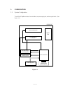
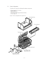
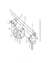
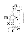
1 - 1 electro-photographic processor paper feed mechanism engine unit hopper plate main high-voltage power supply board sub high-voltage powersupply board power supply unit main control board , , 4mb memory expansion board (okipage 8p only) figure 1-1 1. Configuration 1.1 system configuration the ok...
Page 7
1 - 2 ep unit (type 6) upper cover assy top cover assy heat assy main control board high-voltage power supply board (p6l) high-voltage power supply board (p2h) 1.2 printer configuration the printer unit consists of the following five hardware components: • electro-photographic processor • paper feed...
Page 8
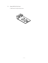
1 - 3 1.3 option(okipage 8p only) (1) 4mb n4a-pcb option memory board.
Page 9
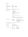
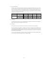
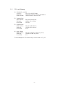
1 - 4 1.4 specification (1) type desktop (2) outside dimensions height 5.9” (150 mm) (excludes protruding width 12.2” (310 mm) portion) depth 7.5” (191 mm) (3) weight 3.8 kg (4) development method dry non-magnetic development system exposure method led stationary head (5) paper used • standard paper...
Page 10
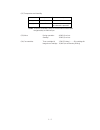
1 - 5 (12) temperature and humidity temperature during operation in storage 10 to 32 ˚c –10 to +43 ˚c 20 to 80% rh (relative humidity) 10 to 90% rh (relative humidity) no condensation is permissible. Humidity caution: temperature and humidity in storage are measured with the okipage 8p/8w being pack...
Page 11
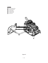
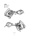
1 - 6 1.5 safety standards 1.5.1 certification label the safety certification label is affixed to the following location of the okipage 4w plus: 1.5.2 warning label warning labels are affixed to the locations that may cause bodily injury. During maintenance, do work with enough care while following ...
Page 12: Operation Description
2. Operation description.
Page 13
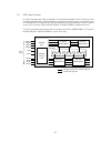
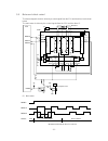
2 - 1 2. Operation description the okipage 8p/8w consists of a main control board, a high-voltage power supply board, a power supply unit, and an electro-photographic processor. The okipage 8p/8w receives print data from a higher-level interface and sequentially stores it in memory. The okipage 8p/8...
Page 14
2 - 2 figure 2-1 block diagram (okipage 8p/8w) plunger led head main motor pj head1 head2 5v 0v 0v motor motor driver mtd2005f eeprom 1kb cpu (nkk 3 or 5) serial i/f data bus (x 16) address bus cent ls07 +26v +5v 0v 0vp power hivol hivol2 hc244 lsi lc26023a rst osc 7mhz osc 10mhz m-rom 4m x 16 mask ...
Page 15
2 - 3 controls dram. Built-in device function dram controller transfers image data from parallel i/f to dram, from dram to a video output port and between cpu and dram. Video output port led stb output port generates various control timings for monitoring paper feeding and a paper size. Dma controll...
Page 16
2 - 4 (2) program rom program rom contains a program for the equipment. Eprom is used as program rom. When mask rom in the one-chip cpu explained in (1) above is valid, the eprom is not mounted. (for details on short wiring setting, see section 7.2.) (3) dram dram is used as resident memory. (4) eep...
Page 17
2 - 5 used to generate a logic circuit and a high voltage. Used to drive the motor and electromagnetic clutch. Output voltage application +5 v +26v output application ch db sb cb tr voltage –1.3 kv –265 v/+265 v –520 v/ 0 v +400 v/–1.3 kv +500 v ~ +3.5 kv/–750 v voltage to be applied to a charge rol...
Page 18
2 - 6 figure 2-2 (2) sensors the high-voltage power supply board consists of the high-voltage power supply circuit that supplies power to the electro-photographic processor system and the photosensor that detects a paper feeding system and toners. Figure 2-2 shows the sensor layout drawing. Sensor f...
Page 19
2 - 7 2.4 electro-photographic processor the electro-photographic processor prints out the image data to be sent from the main control board on sheets of paper. Figure 2-3 shows the layout drawing of the electro-photographic processor. (1) image drum unit the image drum unit makes a toner adhere to ...
Page 20
2 - 8 figure 2-3 layout drawing of electro-photographic processor exit roller heat roller (ø 19.910) 6.85 10 off on 26.50 outlet sensor cleaning roller (ø 9.000) charge roller (ø 9.000) 6.77 led head drum roller (ø 16.000) developing roller (ø 14.000) 17.23 12.72 23.18 20.32 64.60 single tray transf...
Page 21
2 - 9 main motor electromagnetic clutch off on hopping roller non-rotation rotation non-rotation regist gear drum gear operation warm-up hopping prinitng non-rotation rotation rotation rotation rotation rotation normal rotation reverse rotation off (3) pulse motor (main) this pulse motor of 48 steps...
Page 22
2 - 10 figure 2-4 schematic drawing of okipage8p/8w paper feeding exit roller heat roller transfer roller cleaning roller ch roller drum roller developing roller outlet sensor paper sensor hopping roller tray printing feed roller manual feed sensor manual printing 2 roller to be driven by reverse ro...
Page 23
2 - 11 2.5 electro-photographic process (1) electro-photographic process the electro-photographic process is outlined below. 1 charging the surface of the opc drum is charged negatively and uniformly by applying the dc voltage to the ch roller. 2 exposure light emitted from the led head irradiates t...
Page 24
2 - 12 figure 2-5 flow for electro-photographic process control signal exposure transfer paper supply charging paper delivery paper feeding fusing cleaning development paper sensor led head power supply charge roller power supply transfer roller cleaning roller paper eject roller outlet sensor power...
Page 25
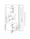
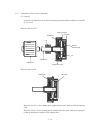
2 - 13 2.5.1 explanation of each process operation (1) hopping as shown in the figure below, the clutch for hopping is turned on/off according to current on/ off to a coil. When the clutch is off when the clutch is on when the clutch is on, the hopping gear engages with the clutch plate to rotate th...
Page 26
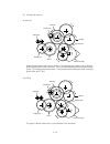
2 - 14 b" b' b hopping gear gear a pulse motor (main) planetary gear idle gear triple gear transfer gear regist gear a" a' a hopping gear gear a pulse motor (main) planetary gear idle gear triple gear transfer gear regist gear rotate the pulse motor (main) in the a direction. The planetary gear rota...
Page 27
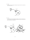
2 - 15 led head charge roller led head image drum paper opc drum high- voltage power supply charge roller opc drum high- voltage power supply (3) charging charging is performed by applying dc voltage to the charge roller that is in contact with the surface of the opc drum. (4) exposure light emitted...
Page 28
2 - 16 2 the toner applied to the developing roller is thin-coated by the developing blade. 3 a toner adheres to the exposure part of the opc drum in the contact part between the opc drum and developing roller. This causes the electrostatic latent image to be changed to a visible image. (5) developm...
Page 29
2 - 17 opc drum transfer roller paper high-voltage power supply (6) transfer the transfer roller is composed of conductive sponge material. This roller is set so that the surface of the opc drum and sheets of paper will adhere closely. A sheet of paper is placed on the surface of the opc drum and th...
Page 30
2 - 18 cleaning roller opc drum transfer roller high-voltage power supply separation claw heater heater roller thermistor pressure spring back-up roller (7) fusing the transferred unfused toner image is fused to a sheet of paper because heat and pressure are applied when it passes between the heat r...
Page 31
2 - 19 2.6 paper jam detection the okipage 8p/8w monitors the paper status when the power supply is on and during printing. In the following cases, the okipage 8p/8w interrupts the printing process as a paper jam. Printing can be recovered by opening the cover, removing the jammed paper, and closing...
Page 32
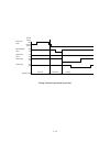
2 - 20 off reverse rotation off on pulse motor (main) electromagnetic clutch off on manual feed sensor off on paper sensor off on operation mode warm-up paper feed printing outlet sensor normal rotation timing chart for paper feed (tray feed).
Page 33
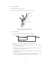
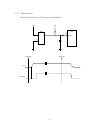
2 - 21 2.7 toner low detection • hardware configuration of toner sensor the figure below shows the hardware configuration of the toner sensor. Caution: the toner sensor is not monitored when the drum is inactive. (a) when the toner-low state continues twice, toner low occurs. (this state is monitore...
Page 34
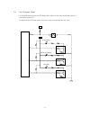
2 - 22 (2) the basic rotation cycle of the toner sensor is as follows: 2.8 cover open opening the stacker cover turns off the microswitch on the high-voltage power supply board to suspend +5 v supply to the high voltage power supply. This results in the stop of all high-voltage outputs. At the same ...
Page 35
2 - 23 2.9 detecting id existence in this model, a micro switch may be activated, applying a high voltage to the machine under a state where the cover is slightly opened. In this case, there is a fear that, when a user insert his hand through the opening, he may be shocked unless an id has been inst...
Page 36
2 - 24 okipage 8p/8w id not installed / toner sensor error draft for specification 1. Toner sensor error/id not installed state should not be stored in the eeprom. 2. A shift to id not installed and toner sensor error shall be made at cover open or close. Power on abnormal toner sensor waveform id n...
Page 37
2 - 25 manual light medium- light medium medium- heavy heavy special1 (china) special2 (swedish archive) ohp light medium- light medium medium- heavy heavy special1 (china) special2 (swedish archive) ohp media type tray feeding tray paper size excutive letter legal 14 legal 13 a4 jis b5 a5 a6 monarc...
Page 38: Parts Replacement
3. Parts replacement.
Page 39
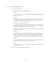
3 - 1 3. Parts replacement this chapter explains how to replace parts, assemblies, and units in the field. The replacement procedures to be explained here include dismounting, not mounting. When mounting parts, assemblies, and units, reverse the dismounting steps. 3.1 precautions for parts replaceme...
Page 40
3 - 2 [maintenance tools] table 3-1 lists the maintenance tools necessary for parts replacement. Table 3-1 maintenance tools no. No. 1-100 philips screwdriver q'ty use remarks maintenance tools 1 2 3 4 5 6 7 no. 2-100 philips screwdriver no. 3-100 philips screwdriver no. 5-200 screwdriver digital mu...
Page 41
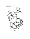
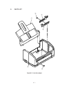
3 - 3 3.2 parts layout this section explains the layout of main parts. [upper cover assy] figure 3-1 hopper plate guide side (r) guide side (l) spur gear (a) upper cover.
Page 42
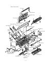
3 - 4 [base frame unit] figure 3-2 ep unit (type 6) power sensor e pulse motor (main) hopping roller roller holder magnet h (hopping shaft) hopping shaft assy side plate m registration roller heat assy idle gear heat paper holder paper guide (r) transfer roller pressure roller (b) (back up roller) t...
Page 43
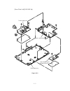
3 - 5 [base plate unit](okipage 8p) figure 3-3-1 high voltage power supply board p6l base plate assy power supply unit main control board.
Page 44
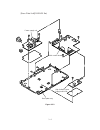
3 - 6 high voltage power supply board p6l base plate assy power supply unit main control board [base plate unit](okipage 8w) figure 3-3-2.
Page 45
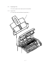
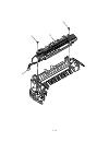
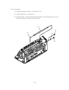
3 - 7 3.3 replacing parts this section explains how to replace parts and assemblies. 3.3.1 hopper plate (1) remove two claws and dismount hopper plate 1 . 1.
Page 46
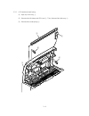
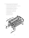
3 - 8 3.3.2 led head and head spring (1) open top cover assy 1 . (2) dismount the left clamp and led head 2 . Then, dismount flat cable assy 3 . (3) dismount two head springs 4 . 2 1 4 4 3.
Page 47
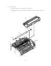
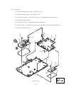
3 - 9 3.3.3 transfer roller (1) open top cover assy 1 and dismount ep unit (type 6) 2 . (2) remove the right claw. Then, dismount transfer roller 3 , two regist bearings 4 , and gear t 5 . 1 2 3 4 4 5 label.
Page 48
3 - 10 3.3.4 upper cover assy (1) turn off the power switch and unplug the ac cord from the ac socket. (2) disconnect interface cable 1 . (3) open top cover assy 2 and dismount ep unit (type 6) 3 . (4) move paper guide (l) 4 and paper guide (r) 5 on the rear of the printer to the center. (5) remove ...
Page 49
3 - 11 3.3.5 high-voltage power supply board (p2h/ p6l) (1) dismount upper cover assy. (see section 3.3.4.) (2) remove three screws 1 and remove the cover 2 and draw out high-voltage power supply board 3 . (3) disconnect all the cables 4 from high-voltage power supply board 3 and dismount high- volt...
Page 50
3 - 12 3.3.6 top cover assy and flat cable assy (1) dismount the upper cover assy. (see section 3.3.4.) (2) dismount the led head. (see section 3.3.2.) (3) press the left clamp outward and dismount the engagement and top cover assy 1 . (tension spring 2 also comes off at the same time.) (4) disconne...
Page 51
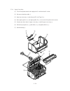
3 - 13 3.3.7 paper holder (1) dismount the upper cover assy. (see section 3.3.4.) (2) dismount paper holder 1 . (3) unlock and dismount paper guide (l) 2 and paper guide (r) 3 . (4) remove the claw and dismount hopper spring 4 . (5) remove the claw and dismount stopper spring 5 . 1 2 3 4 5.
Page 52
3 - 14 3.3.8 side plate m and idle gear perform parts replacement while making the base frame assy stand so that side plate m will face upward. (1) dismount the upper cover assy. (see section 3.3.4.) (2) remove two screws 1 and two claws, then dismount plate side m 2 . (3) dismount earth plate 3 , t...
Page 53
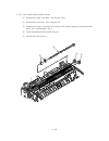
3 - 15 3.3.9 heat assy this section explains how to dismount the heat assy and parts in the assy. (1) dismount the upper cover assy. (see section 3.3.4.) (2) dismount the high-voltage power supply board. (see section 3.3.5.) (3) remove two screws 1 , disconnect connector 2 , and dismount heat assy 3...
Page 54
3 - 16 1 2 1 3.
Page 55
3 - 17 7 9 8 8 c 5 a b 0 6 d d 4 voltage display side.
Page 56
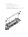
3 - 18 3.3.10 drive shaft e (eject) and eject roller (1) dismount the upper cover assy. (see section 3.3.4.) (2) dismount top cover assy. (see section 3.3.6.) (3) remove two screws 1 from heat assy (section3.3.9), life the heat assy, and dismount idle gear e (a) 2 and idle gear e (b) 3 . (4) unlock ...
Page 57
3 - 19 3.3.11 pressure roller b (back up roller) (1) dismount the upper cover assy. (see section 3.3.4.) (2) dismount the high-voltage power supply board. (see section 3.3.5.) (3) dismount the heat assy. (see section 3.3.9.) (4) dismount the engagement with the left ground, then pressure roller b 1 ...
Page 58
3 - 20 3.3.12 separator guide (1) dismount the upper cover assy. (see section 3.3.4.) (2) dismount the high-voltage power supply board. (see section 3.3.5.) (3) remove four screws 1 . (4) dismount inlet 2 from base frame 3 . 2 > insert a screwdriver into the hole on the side of base frame 3 , remove...
Page 59
3 - 21 1 1 3 1 1 2 6 8 9 4 a 4 4 b b a 7 screw driver (-) screw driver clamp lever cn2 okipage 8p.
Page 60
3 - 22 1 1 3 1 1 2 6 8 9 4 a 4 4 b b a screw driver (-) screw driver clamp lever cn2 okipage 8w.
Page 61
3 - 23 3.3.13 pulse motor (main) (1) dismount the upper cover assy. (see section 3.3.4.) (2) dismount the high-voltage power supply board. (see section 3.3.5.) (3) dismount side plate m. (see section 3.3.8.) (4) dismount the base frame. (see section 3.3.12.) (5) remove two screws 1 and dismount puls...
Page 62
3 - 24 3.3.14 hopping shaft assy (1) dismount the upper cover assy. (see section 3.3.4.) (2) dismount the high-voltage power supply board. (see section 3.3.5.) (3) dismount the base frame. (see section 3.3.12.) (4) dismount the paper holder assy. (see section 3.3.7.) (5) dismount the sheet guide. (s...
Page 63
3 - 25 3.3.15 resist roller (1) dismount the upper cover assy. (see section 3.3.4.) (2) dismount idle gear r 3 and gear r 4 . (3) move resist roller 1 to the right and dismount it by lifting. (two resist bearings 2 also come off at the same time. Take care not to lose them.) 2 1 3 2 4.
Page 64
3 - 26 3.3.16 paper sensor e, paper sensor exit and toner sensor assy (1) dismount the upper cover assy. (see section 3.3.4.) (2) dismount the high-voltage power supply board. (see section 3.3.5.) (3) dismount the base frame. (see section 3.3.12.) (4) dismount the paper holder assy. (see section 3.3...
Page 65
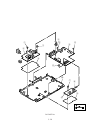
3 - 27 3.3.17 base plate (1) dismount the upper cover assy. (see section 3.3.4.) (2) dismount the base frame. (see section 3.3.12.) (3) remove two screws 1 , disconnect connector 2 , and dismount power supply unit 3 . (4) dismount insulation sheet 4 . (5) remove five screws 5 and dismount main contr...
Page 66
3 - 28 okipage 8w 1 1 2 5 5 5 8 a 9 7 0 6 3 4.
Page 67: Adjustment
4. Adjustment.
Page 68
4 - 1 4. Adjustment this chapter explains adjustment necessary when a part is replaced. This adjustment is made by changing the parameters values set in eeprom on the main control board. The printer driver or maintenance utility can be used to change these values. Only servicemen and maintenance per...
Page 69
4 - 2 4.1.2 engine maintenance utility see appendix d. 4.2 adjustment when replacing a part the table below lists the parts that requires adjustment when they are replaced. Luminous intensity display 027 135 figure 4-2 part to be replaced adjustment led head ep unit reset the drum counter. (refer to...
Page 70
4 - 3 4.2.2 uploading and downloading eeprom data when the main control board is replaced, eeprom data must be reflected on a new main control board. Use “eeprom operations” in the option tab of the maintenance utility to reflect eeprom data on the new main control board. (see figure 4-4.) reflect e...
Page 71: Periodical Maintenance
5. Periodical maintenance.
Page 72
5 - 1 5. Periodical maintenance 5.1 periodical replacement parts table 5-1 lists the part and unit to be replaced periodically. Table 5-1 routine replacement parts toner cartridge (type 6) part name replacement time part to be checked simultaneously remarks ep unit (type 6) when "toner low" is displ...
Page 73
5 - 2 led head cleaner led lens array figure 5-2 (1) set the led head cleaner in the led lens array, as shown in the figure below, and slide the cleaner left and right several time to clean the head. Caution: do not press the led head cleaner against the led lens array..
Page 74: Troubleshooting Procedures
6. Troubleshooting procedures.
Page 75
6 - 1 6. Troubleshooting procedures 6.1 troubleshooting tips (1) check the basic check points written in the user’s manual. (2) gather detailed failure information as much as possible from the customer. (3) check the printer under the condition close to that under which the failure occurred. 6.2 che...
Page 76
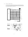
6 - 2 led functions status error (red) ready (amber) remark manual feed (amber) flash 1: slow blinking flash 2: blinking flash 3: fast blinking ready during suspending data pro- cessing (in off-line) (data is left in the buffer) during receiving data or pro- cessing data manual request low toner war...
Page 77
6 - 3 trouble trouble indicated by the message displayed on the status monitor. Image problem (or trouble not displayed on the status monitor) perform detailed troubleshooting according to the troubleshooting flow. (see section 6.5.2.) troubleshoot according to section 6.5.3. Troubleshoot according ...
Page 78
6 - 4 status code category status message display content remedy table 6-1 warming-up status online (ready) status power save status the toner amount of the toner cartridge is small. The ep unit is not installed or the toner sensor is faulty. Life of ep drum the paper is in the manual feed mode. Pri...
Page 79
6 - 5 status code category status message display content remedy table 6-1 (cont'd) 30 00 31 00 32 00 33 00 42 00 4f 00 40 01 40 10 60 10 60 30 paper of improper size was fed. 2.52" (64 mm) l 15.77" (400.56 mm) a paper jam occurred when sheets of paper were being supplied. A paper jam occurred durin...
Page 80
6 - 6 status code category status message display content remedy table 6-1 (cont'd) 60 40 60 60 60 80 60 90 60 91 60 92 60 c0 an error occurred during eeprom check. An error occurred during option ram check. A heater timeout error occurred. A thermistor error occurred. The thermistor is open. A ther...
Page 81
6 - 7 6.5.2 status message troubleshooting some failures cannot be corrected according to the status message trouble list. Troubleshoot these failures according to the following troubleshooting flowcharts: caution: when replacing the main control board troubleshooted according to the troubleshoot- i...
Page 82
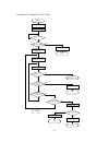
6 - 8 1 the okipage 8p/8w malfunctions after the power supply has been turned on. • turn the power supply off, then on again. • is the led lamp on? • no is the ac cable connected correctly? • no connect the ac cable correctly. • yes is +5 v supplied between cn1 pin 7 and cn1 pin 13 of the high-volta...
Page 83
6 - 9 [jam error] 2 -1 paper input jam • does a paper input jam occur when the power supply is turned on? • yes is the jammed paper on paper sensor e? • yes remove the jammed paper. • no is paper sensor e (manual feed/paper) operating normally? • no replace paper sensor e (manual feed or paper). • y...
Page 84
6 - 10 [jam error] 2 -2 paper feed jam • does a paper feed jam occur when the power supply is turned on? • yes is the jammed paper on paper sensor e (paper/exit)? • yes remove the jammed paper. • no is paper sensor e (exit/paper) operating normally? • no replace paper sensor e (exit or paper). • yes...
Page 85
6 - 11 3 paper size error • is the paper of the specified size being use? • no use paper of the specified size. • yes is paper sensor e (paper) operating normally? • no replace paper sensor e (paper) or clean the inlet sensor on the high-voltage power supply board. • yes is the paper sensor (exit) o...
Page 86
6 - 12 4 heat assy error • turn the power supply off, then on again. • does the halogen lamp of the heat assy go on? • no is the halogen lamp or thermostat disconnected? • yes replace the heat assy, halogen lamp, or thermostat. • no replace the power supply unit. • yes are the cn2 connectors of the ...
Page 87
6 - 13 a light or blurred images entirely b dark background density c blank paper d black vertical stripes e cyclical defect f white vertical belts or streaks figure 6-3 image problems 6.5.3 image troubleshooting this section explains how to troubleshoot when an image problem is output as a result o...
Page 88
6 - 14 1 an image is light or blurred entirely. • is the toner low? (is "toner low" being displayed?) • yes supply a toner. • no is the specified paper being used? • no use the specified paper. • yes is the lens of the led head dirty? • yes clean the led head. • no is the led head installed correctl...
Page 89
6 - 15 2 dark background density • has the opc drum being exposed to external light? • yes set the opc drum in the okipage 8p/8w and wait for about 30 minutes. • no is the heat roller of the heat assy dirty? • yes clean the heat roller. • no is the terminal of the ep unit in correct contact with the...
Page 90
6 - 16 4 vertical black belt/stripe • replace the ep unit. • has this error been recovered? • yes end caution: after replacing the ep unit, reset the drum counter. (refer to "replacing the drum cartridge" in "user's manual".) • no replace the led head. • has this error been recovered? • yes end caut...
Page 91
6 - 17 6 a blank paper is output. • is the contact plate of the transfer roller in correct contact with the high-voltage power supply board? • no contact the contact plate of the transfer roller correctly. • yes replace the transfer roller. • has this error been recovered? • yes end • no is the term...
Page 92
6 - 18 7 poor fusing • is the specified paper being used? • no use the specified paper. (xerox 4200 (20 lbs)) • yes is the bias spring normal? (tension: 3.25 kg) • no replace the bias spring. • yes are the heater connector of the heat assy and the cn1 connector of the power supply unit connected cor...
Page 93
6 - 19 8 vertical white belt/spripe • is the lens of the led head dirty? • yes clean the led head. • no is the contact plate of the transfer roller in correct contact with the high-voltage power supply board? (see figure 6-5 e .) • no contact the contact plate of the transfer roller correctly. • yes...
Page 94
6 - 20 figure 6-4 contents a : toner supply roller b : developing roller c : charge roller d : cleaning roller e : transfer roller f : heat roller a e d f b c.
Page 95
6 - 21 figure 6-5 contents a : toner supply roller b : developing roller c : charge roller d : cleaning roller e : ground (drum) a b d c e.
Page 96: Wiring Diagram
7. Wiring diagram.
Page 97
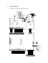
7 - 1 7. Wiring diagram 7.1 (a)interconnect signal diagram (okipage 8p) 14 30 1 16 option (not used) main control board (nma- pcb) power supply unit high-voltage power supply board p2h high-voltage power supply board p6l cent (parallel interface) head1, head2 (led head) 13 29 2 17 36 18 19 1 1 stb-n...
Page 98
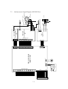
7 - 2 7.1 (b)interconnect signal diagram (okipage 8w) main control board (hbmc-2 pcb) power supply unit high-voltage power supply board p2h high-voltage power supply board p6l cent (parallel interface) head1 head2 36 18 19 1 1 stb-n 2 pdata1-p 3 pdata2-p 4 pdata3-p 5 pdata4-p 6 pdata5-p 7 pdata6-p 8...
Page 99
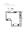
7 - 3 7.2 pcb layout 7.2.1 main control board (nma pcb) (okipage 8p) hivol2 sw1 1 2 hivol cent led1 led2 led3 head2 19 1 1 12 head1 14 1 36 18 power 1 1 8 2 cn7 option pj 1 1 2 4.
Page 100
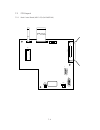
7 - 4 7.2 pcb layout 7.2.2 main control board (hby pcb) (okipage 8w) cn10 ic2 1 2 cn1 cn4 head2 19 1 1 12 head1 14 1 36 18 cn2 1 1 8 2 cn7 cn8 1 1 2 4.
Page 101
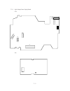
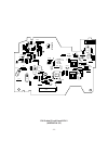
7 - 5 7.2.3 high-voltage power supply board p2h ps2 ps1 ps4 cvsw ps3 cn7 cn1 p6l cn1.
Page 102: Parts List
8. Parts list.
Page 103
8 - 1 8. Parts list figure 8-1 cover assy upper 7 6 5 4 1 2 *1.
Page 104
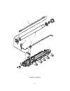
8 - 2 1 cover-upper 1 40412501 1 okipage 8p cover-upper 2 40412601 1 okipage 8w 2 lens 1 40413101 1 okipage 8p lens 2 40413201 1 okipage 8w 3 switch 40413001 1 okipage 8p 4 guide side (l) 2pp4128-1256p1 1 5 guide slide (r) 2pp4128-1257p1 1 6 gear spur a 4pp4128-1260p1 1 7 plate-hopper 40412901 1 tab...
Page 105
8 - 3 figure 8-2 base frame unit d d e f c [ u r j e d i c b a 0 9 8 7 5 o 6 3 3 1 2 i g h f k n p l l q s z k g w t t o m t t z y t v l \ ] ^ b.
Page 106
8 - 4 table 8-2 base frame unit no. Part name part no. Q'ty remarks 1 frame unit assy 40593201 1 2 high-voltage power supply board p2h 40607401 1 3 paper sensor e 3pp4083-1191p1 2 4 5 separator assy 40721301 1 6 compression spring s 4pp4083-1246p1 1 7 toner sensor assy 3pa4083-1193g1 1 8 pulse motor...
Page 107
8 - 5 35 bias spring (l) (back up roller) 4pp4083-1136p1 1 36 bearing bu (back up roller) 3pp4083-1161p1 2 37 pressure roller b (back up roller) 40594601 1 38 paper guide (r) 40249501 1 39 paper guide (l) 40249401 1 40 paper holder 1pp4083-1231p1 1 41 paper sensor exit 3pp4083-1192p1 1 42 hopper spr...
Page 108
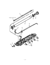
8 - 6 figure 8-3 heat assy 2 1 8 5 3 4.
Page 109
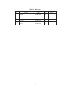
8 - 7 no. Part name part no. Q'ty remarks table 8-3 heat assy 1 heat roller 3pb4083-1202p1 1 2 halogen lamp 40649301 1 120v halogen lamp 40649302 1 230v 3 thermostat 4pb4083-1204p1 1 4 thermistor 4pb4083-1205p1 1 5 heat cord 4pb4083-1213p1 1.
Page 110
8 - 8 figure 8-4-1 base plate unit (okipage 8p) 9 3 4 2 a 0 1 7.
Page 111
8 - 9 6 3 4 2 a 0 1 7 figure 8-4-2 base plate unit (okipage 8w).
Page 112
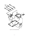
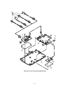
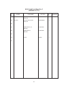
8 - 10 1 base plate assy 40592201 1 2 insulation sheet a 40722501 1 3 power supply unit 4yb4049-1853p1 1 120v power supply unit 4yb4049-1854p1 1 230v 4 main control board 40681602 1 for op 8w (hby-) main control board 40433802 1 for op 8p (hby-) 5 6 program rom 40681701 1 op8w eprom 7 ac cord 3ys401...
Page 113: Appendix
Appendix.
Page 114
A - 1 appendix a local printing (1) the following operation enables the okipage 8p/8w to print data by itselt. With the cover open, turn on the ac switch and then close the cover. The following print patterns are printed..
Page 115
B - 1 appendix b parallel interface (1) connector • printer side : 36-pin receptacle type: 57re-40360-730b-d29a (daiichi denshi) or equivalent • cable side : 36-pin plug type: 57-30360 (daiichi denshi) or equivalent (2) cable • cable length : 6 feet (1.8 m) max. (ieee std 1284-1994 compliant is reco...
Page 116
B - 2 (3) parallel i/f signals pin no. Signal name direction function (compatible mode) 1 2 3 4 5 6 7 8 9 10 11 12 13 14 15 16 18 19 30 31 32 33 34 35 36 data strobe data bit - 1 data bit - 2 data bit - 3 data bit - 4 data bit - 5 data bit - 6 data bit - 7 data bit - 8 acknowledge busy paper end sel...
Page 117
B - 3 (4) signal level • low : 0 v to +0.8 v • high : +2.4 v to 5.0 v (5) interface circuit • 8p • 8w a) receiving circuit a) receiving circuit b) sending circuit b) sending circuit r = 3.3k Ω (1.0-k Ω strobe) +5v r (open collector) +5v 3.3k Ω (6) timing charts a) data receiving timing (compatible m...
Page 118
B - 4 c) data sending timing (nibble mode) acknowledge busy 6 7 4 5 2 3 data bit 3 data bit 7 fault 6 7 4 5 2 3 data bit 0 data bit 4 select . / , - * + data bit 1 data bit 5 paper end & ' . / $ % , - " # * + data bit 2 data bit 6.
Page 119
C - 1 appendix c maintenance utility 1. Outline of maintenance utility the maintenance utility is an application program that operates on microsoft windows 3.1 or higher. The maintenance utility has the following functions: • transmission of menu setting command to initialize and change setting valu...
Page 120
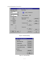
C - 2 4. Detail of each function 4.1 engine menu setting engine menu setting is used to set, display, and change the following menu items: (see figure d-1.) (1) print position used to adjust the print start position. (2) led head marking no. Used to adjust the exposure time of the led head. (3) led ...
Page 121
C - 3 (1) drum count number of revolutions of mounted ep drum (2) total drum count total number of revolutions of ep drum after shipment (3) page count total number of printed pages after shipment clicking the "reset" button cleans each counter. (4) reset all used to clear all counters. 4.3 printer ...
Page 122
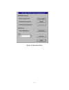
C - 4 4.6 about about is used to display the following information: engine maintenance utility version information printer version information and memory size information printer device id information see figure c-4. 4.7 reload reload is used to reload menu setting values. 4.8 exit clicking the exit...
Page 123
C - 5 figure c-1 main menu dialog figure c-2 test print dialog.
Page 124
C - 6 figure c-3 option menu dialog.
Page 125
C - 7 figure c-4 about dialog.
Page 126
Xxxxxxxxth oki data corporation 4-11-22, shibaura, minato-ku, tokyo 108, japan tel: (03) 5445-6162 fax: (03) 5445-6189.
Page 127
All specifications are subject to change without notice. Okipage8 p led page printer troubleshooting manual with component parts list (oda/oel/int).
Page 128
Contents 1. Outline..................................................................................................... 1 2. Tools ........................................................................................................ 1 3. Circuit description .........................................
Page 129
- 1 - 1. Outline this manual has been written to provide guidance for troubleshooting of the okipage8p printer (primarily for its printed circuit boards), on an assumption that the reader is knowledgeable of the printer. Read the maintenance manual for this printer if necessary. Note: 1. High voltag...
Page 130
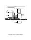
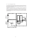
- 2 - 3. Circuit description 3.1 outline the circuit of okipage8p consists of a main control board, a main high voltage power supply board, a sub-high voltage power supply board and a power supply unit. The block diagram is shown in fig. 3-1. The main control board controls the reception and transmi...
Page 131
- 3 - figure 3-1 okipage8p block diagram option o p t i o n pcb n4a- dram 4mb dram 2mb cpu (nkk3 or 5) 0v red amber amber dram 1m x 16 dram 1m x 16 serial i/f ac (120v/ 230v) heater (halogen lamp) parallel i/f data bus (x16) address bus m-rom 4m x 16 high voltage power unit p6l high voltage power un...
Page 132
- 4 - 3.2 cpu and memory (1) cpu (nkk3 or nkk5) cpu core risc cpu (mips r3000) cpu clock 7.067 mhz, internal cpu clk 28.268 mhz data bus width external 16 bits, internal 32 bits (2) program rom rom capacity 8m-bytes (mask rom) rom type 64mbits (4m x 16 bits) access time 100 nsec (3) resident ram ram...
Page 133
- 5 - figure 3-2 block diagram of cpu & memory in okipage8p cpu cs0 cs0 rd ras0 rd/wr cas0, 1 ras1, 2 cas0, 1 wr main control board ras0 ras1 ras2 cas0 cas1 dram (1m x 16 bits) dram 4m byte ras1, 2 wr d00 to d15 a00 to a25 mask rom (4m x 16 bits) option board cas0,1.
Page 134
- 6 - 3.3 reset control when power is turned on, rst-n signal is generated by rst. Power off power on +5v cl rst-n cpu 172 1 2 3 rst +5v +5v rstn.
Page 135
- 7 - instruction start bit operation address data code read (read) 1 10 a5 to a0 write enabled (wen) 1 00 11xxxx write (write) 1 01 a5 to a0 d15 to d0 write all address (wral) 1 00 01xxxx d15 to d0 write disabled (wds) 1 00 00xxxx erase 1 11 a5 to a0 chip erasable (eral) 1 00 10xxxx 3.4 eeprom cont...
Page 136
- 8 - 3.5 centronics parallel interface the cpu sets a busy-p signal to on at the same time when it reads the parallel data (pdata1- p to pdata 8-p) from the parallel port at the fall of pstb-n signal. Furthermore, it makes the store processing of received data into a receive buffer terminate within...
Page 137
- 9 - 3.6 front operator panel front operator panel have three led lamps and a switch on the main control board which is connected to by the cpu. The light from the led lamp can be seen on the lens cover through the led lens. Cpu 5v 5v 0v ready (amber) manual feed (amber) 110 114 113 161 error (red).
Page 138
- 10 - 3.7 led head control an led correcting head, which is capable of correcting the illumination of the led for each dot, is being used in this printer. Led illumination correction function of 16 steps is carried out by using an eeprom which is installed in the lsi that maintains the led illumina...
Page 139
- 11 - the printing operation is carried out in the following sequence. First, the printing data datai3 through datai0 are stored, sequentially shifted, in the shift registers of the led drivers, by the printing data synchronous clock, clocki. Then the printing data stored in shift registers are lat...
Page 140
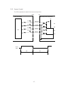
- 12 - 3.8 motor and clutch control the electromagnetic clutch is driven by a control signal from the cpu and the drive circuit shown below. The main motor is driven by the control signals from the cpu and the driver ic. (1) main motor m cpu dmph1p dmon1n motor +5v +5v +5v 23 22 28 15 10 21 20 tab 5...
Page 141
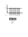
- 13 - (2) motor drive control time t0 to t3 determines the motor speed, while the phase different direction between phase signals dmph1-p and dmph2-p determines the rotation direction. Dmon-n signal control a motor coil current. According to the polarity of the phase signal, the coil current flow a...
Page 142
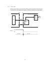
- 14 - 3.9 fuser temperature control for the temperature control by heater control, the variation in the resistance of the thermistor is a/d converted in lsi and the resultant digital value is read and transferred to the cpu. The cpu turns on or off the hton-n signal according to the value of the si...
Page 143
- 15 - flowchart of thermistor circuit check heater off short check timer(t16)set temperature > tn thermistor error check timer (t2) within time thermistor disconnection check timer (t35) within time start to constant temperature control end heater on yes yes yes yes yes no no no no no no no yes yes...
Page 144
- 16 - temperature controlled temperature t heater on off time temperature table thermcmp-n o z heater control mode normal operation fuser error check t 145˚c: 150˚c: 155˚c: 160˚c: 165˚c: paper thickness light medium light medium medium heavy heavy.
Page 145
- 17 - 3.10 sensor control the cpu supervises the state of each sensor every 40 ms. Off tnrsns-n hivol cn1 psin-n psout-n wrsns-n cpu +5v ps1 ps2 ps3 ps4 on transparent shield sensor signal 124 120 122 123 +5v +5v +5v +5v main control board high voltage power supply board.
Page 146
- 18 - 3.11 cover open when the cover is opened, a cover open microswitch is opened. This makes a cvopn-n signal low, thereby the cpu detects that cover is open. Furthermore, opening the cover stops applying a +5v power to the high voltage power supply part, resulting in stopping all high voltage ou...
Page 147
- 19 - 3.12 power supply part (1) power supply unit an ac power from an inlet is input to switching reg. Part .Ac power is converted to a +26 vdc output and +5 vdc output. (2) high voltage power supply board the +5 vdc power supplied to the high voltage power supply part via the cover open microswit...
Page 148
- 20 - control signals and high voltage outputs control signal name level function tr1pwm h/l (pwm) l h/l(pwm) l h/l(pwm) l h l h l h/l(pwm) l h/l(pwm) l h/l(pwm) l makes the part put out a power to tr. Makes the part put out a -750v power to tr. Makes the part put out a -1300 kv power to ch. Makes ...
Page 149
- 21 - 4. Troubleshooting 4.1 troubleshooting table (a) high voltage power supply board note: a malfunction of the power supply is not repaired by an agency. The abnormality to be treated here is that of sensors only. Failure led error(red) manual feed (amber) ready (amber) pc display message flowch...
Page 150
- 22 - (b) main control board failure led error(red) manual feed (amber) ready (amber) pc display message flowchart no. Initialization error and not restored e r r o r 7 1 b - 1 program rom error b - 2 resident ram error b - 3 eeprom error b - 4 fuser error flash3 b - 5 thermister open error b - 5 t...
Page 151
- 23 - 4.2 troubleshooting flowchart a-1 paper input jams occur frequently. • is ps4 (write sensor ) operating normally? • no replace ps4. ▼ • yes is pin1 of pj connector in main control board operating normally? • no replace tr501 or tr502 in main control board. ▼ • yes failure of cpu in main contr...
Page 152
- 24 - a-6 the message “cover open” remains displayed on the pc display. • is cvsw (cover open switch) operating normally? • no replace cvsw. ▼ • yes failure of cpu in main control board. A-7 the message “tonerlow” remains displayed on the pc display. • is ps1 (toner sensor) operating normally? • no...
Page 153
- 25 - b-1 initialization error and not restored • replace rom. ▼ • ok? ▼ • no is the 7.065-mhz clock signal being put out to pin 3 of ocs1? • no replace osc1 (cst 7.065m). ▼ • yes failure of cpu b-2 program rom error • replace rom. B-3 resident ram error • are negative pulses being put out to pin 1...
Page 154
- 26 - on-line off-line busy-p low high b-7 data sent through the parallel i/f cannot be received. • is the signal at pin 11 (busy-p) of cent connector being at low level? • no is the signal at pin 13 (busy-p) of q4 (74ls07) changed as shown below, at data reception? • no failure of cpu ▼ • yes repl...
Page 155
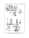
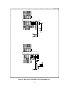
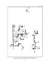
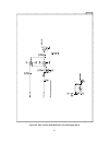
- 27 - 5. Circuit diagram figure 5-1 ~ 5-11 main control pcb (nma-) circuit diagram (rev. 5) figure 5-12 high voltage power supply pcb (p2h-) circuit diagram (rev.2) figure 5-13 high voltage power supply pcb (p6l-) circuit diagram (rev.2) figure 5-14 option memory pcb (n4a-) circuit diagram (rev.2).
Page 156
1 2 34 56 78 9 x y 1 a b c d e f g h a b c d e f g 23 4 5 6 7 8 9 x y - 28 - figure 5-1 main control pcb (nma-1/11) circuit diagram rev.5 2028k/ 3ar3 (1/3) cpu osc2 osc1 vdd18 vdd17 vdd16 vdd15 vdd14 vdd13 vdd12 vdd11 vdd10 vdd9 vdd8 vdd7 vdd6 vdd5 vdd4 vdd3 vdd2 vdd1 vss19 vss18 vss17 vss16 vss15 v...
Page 157
1 2 34 56 78 9 x y 1 a b c d e f g h a b c d e f g 23 4 5 6 7 8 9 x y - 29 - figure 5-2 main control pcb (nma-2/11) circuit diagram rev.5 2028k/ 3ar3 (2/3) cpu bendnp cs0wp tstenp frcmn clrstn wmrstn drdyn breqn scrrqp int2n int1n cdcnn pdt8p pdt7p pdt6p pdt5p pdt4p pdt3p pdt2p pdt1p cstbn initn aut...
Page 158
1 2 34 56 78 9 x y 1 a b c d e f g h a b c d e f g 23 4 5 6 7 8 9 x y - 30 - figure 5-3 main control pcb (nma-3/11) circuit diagram rev.5 dram 5118160j a11/nc a10/nc a9 a8 a7 a6 a5 a4 a3 a2 a1 a0 rasn ucasn lcasn wen oen nc1 nc2 nc3 vcc1 vcc2 vcc3 gnd1 gnd2 gnd3 i/o16 i/o15 i/o14 i/o13 i/o12 i/o11 i...
Page 159
1 2 34 56 78 9 x y 1 a b c d e f g h a b c d e f g 23 4 5 6 7 8 9 x y - 31 - figure 5-4 main control pcb (nma-4/11) circuit diagram rev.5 mtdv mtd2005f phaa nena phab nenb cr refa vsa refb vsb dcay vcc lga lgb vmm1 vmm2 gnd1 gnd2 out1 out2 out3 out4 nalm rsa rsb nc1 nc2 nc3 nc4 nc5 nc6.
Page 160
1 2 34 56 78 9 x y 1 a b c d e f g h a b c d e f g 23 4 5 6 7 8 9 x y - 32 - figure 5-5 main control pcb (nma-5/11) circuit diagram rev.5.
Page 161
1 2 34 56 78 9 x y 1 a b c d e f g h a b c d e f g 23 4 5 6 7 8 9 x y - 33 - figure 5-6 main control pcb (nma-6/11) circuit diagram rev.5.
Page 162
1 2 34 56 78 9 x y 1 a b c d e f g h a b c d e f g 23 4 5 6 7 8 9 x y - 34 - figure 5-7 main control pcb (nma-7/11) circuit diagram rev.5 lsi q1 74hc244 vcc=d5v, ground=0v 1a1 1a2 1a3 1a4 1c 2a1 2a2 2a3 2a4 2c 1y1 1y2 1y3 1y4 2y1 2y2 2y3 2y4 lc26023a clk0 clk1 sqcr sclk dinp doutp resetn answ9 answ8...
Page 163
1 2 34 56 78 9 x y 1 a b c d e f g h a b c d e f g 23 4 5 6 7 8 9 x y - 35 - figure 5-8 main control pcb (nma-8/11) circuit diagram rev.5.
Page 164
1 2 34 56 78 9 x y 1 a b c d e f g h a b c d e f g 23 4 5 6 7 8 9 x y - 36 - figure 5-9 main control pcb (nma-9/11) circuit diagram rev.5.
Page 165
1 2 34 56 78 9 x y 1 a b c d e f g h a b c d e f g 23 4 5 6 7 8 9 x y - 37 - figure 5-10 main control pcb (nma-10/11) circuit diagram rev.5.
Page 166
1 2 34 56 78 9 x y 1 a b c d e f g h a b c d e f g 23 4 5 6 7 8 9 x y - 38 - figure 5-11 main control pcb (nma-11/11) circuit diagram rev.5.
Page 167
1 2 34 56 78 9 x y 1 a b c d e f g h a b c d e f g 23 4 5 6 7 8 9 x y - 39 - figure 5-12 high voltage supply pcb (p2h-1/1) circuit diagram rev.2.
Page 168
1 2 34 56 78 9 x y 1 a b c d e f g h a b c d e f g 23 4 5 6 7 8 9 x y - 40 - figure 5-13 high voltage supply pcb (p6l-1/1) circuit diagram rev.2.
Page 169
1 2 34 56 78 9 x y 1 a b c d e f g h a b c d e f g 23 4 5 6 7 8 9 x y - 41 - figure 5-12 option memory pcb (n4a-1/1) circuit diagram rev.2 dram 5118160j a11/nc a10/nc a9 a8 a7 a6 a5 a4 a3 a2 a1 a0 rasn ucasn lcasn wen oen nc1 nc2 nc3 vcc1 vcc2 vcc3 gnd1 gnd2 gnd3 i/o16 i/o15 i/o14 i/o13 i/o12 i/o11 ...
Page 170: Component Parts List
- 1 - component parts list.
Page 171
- 2 - drawing list main control board (nma pcb, rev. 5) 40433801ya high voltage power supply board (p2h pcb, rev.2) 40607401ya high voltage power supply board (p6l pcb, rev.2) 40605601ya option board (n4a pcb, rev.2) 40559001ya.
Page 172
- 3 - nma printed circuit board rev.5 (40433801ya-1/2) head1 head2 14 13 2 1 1 2 11 12 1 19 18 36 cent osc2 osc1 r1 1 1 2 4 r2 r94 motor pj eeprom rst r15 c12 q2 c6 c7 cpu power hivol 1 8 23 22 1 2 1 2 1 c4 c1 tr4 r98 r59 c17 c18 c19 r97 r63 r64 r65 r66 r67 d3 r56 r57 r68 r69 tr3 r3 c21 r60 c20 r92 ...
Page 173
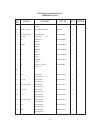
Ref. Symbol type/name part no. Q'ty remarks no. - 4 - d1,d3,d501 d2 r554 r97,r547,r548 r98,r556 r44,r55 r558 r54 r579 r557 r42 r511 r43 r580 r593 r15,r64,r66,r69,r74, r87,r502,r503,r559, r478,r595,r596,r599,r611 ss100ma80vacp d-signal -c rd 3.3m-b2 d-zener -c cr/rk73h/erj/mcrf102 res-met rn -c cr/rk...
Page 174
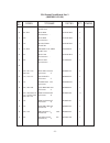
Ref. Symbol type/name part no. Q'ty remarks no. - 5 - 18 19 20 21 22 23 24 25 26 27 28 29 30 31 32 33 34 r61~r63,r65,r67,r68, r549, r560 r38 r36 r608~r610 r57 r501,r597 r41,r48~r50 r563,r564,r581~r583, r 590~r592 r585 r598 r605,r606 r573,r574,r584,r586,r587 r518~r522,r566~r571 r70~r73,r75~r86,r95,r5...
Page 175
Ref. Symbol type/name part no. Q'ty remarks no. - 6 - 35 36 37 38 39 40 41 42 43 44 45 46 47 48 49 50 51 r37,r46,r47 r602 r59,r60,r545,r555,r620 r9,r39,r40,r603,r614,r615 r604 r51,r52 r607 r10~r14,r45,r92,r93,r96, r510,r527,r531,r532,r600, r601,r612,r613,r616,r618 r58 r529,r530,r550,r552,r561, r562 ...
Page 176
Ref. Symbol type/name part no. Q'ty remarks no. - 7 - 52 53 54 55 56 57 58 59 60 61 62 63 64 65 66 67 68 c9 c517,c525,c534,c535 c511,c514,c521,c531,c533, c551,c552 c553 c536,c537,c544~c546 c543 c547 c540 c12,c14,c16~c19,c20,c501~ c504,c509,c522,c526,c529, c538,c541,c532,c548~c550 c21,c22,c24,c27,c28...
Page 177
Ref. Symbol type/name part no. Q'ty remarks no. - 8 - 69 70 71 72 73 74 75 76 77 78 79 80 81 82 83 84 85 q4 lsi q1 q2 q3 mtdv rst dram eeprom cpu rom tr4 tr1,tr502 tr506 tr2,tr501,tr503~tr505 74ls07fp digital ic-bip-s lc26023a-na5 digital ic-mos- 74hc244fp digital ic-mos-s tl431clp/njm431l-t3 analog...
Page 178
Ref. Symbol type/name part no. Q'ty remarks no. - 9 - 86 87 88 89 90 91 92 93 94 95 96 97 98 99 100 101 102 103 tr3 sw1 cent head2 head1 option pj motor power hivol2 hivol osc1 osc2 f1 2sd1623s tr-npn/l-freq -c soa-113hs switch-push - 57re-40360-830b-d29 connector-sqr - sld12s-2 connector-pcb - sld1...
Page 179
- 10 - ref. Symbol type/name part no. Q'ty remarks no. 104 105 106 107 108 109 110 111 sel3213c/gl3hd47 photo-led - sel3913kyz/gl3hy47bc photo-led - smcd23/twvf23-210 conn par- - smcd6/twvf6-55 conn par- - cap-led 650a0103m0001 650a0203m0001 2381003p0003 2381003p0005 40666901 1 2 1 1 3 nma printed c...
Page 180
- 11 - p2h printed circuit board rev.2 (40607401ya-1/2) d84 d58 d56 d61 d60 d52 d67 d69 d68 d71 d76 ext d59 d55 c240 r124 led c237 c110 d63 tr d62 q15 d72 d87 r48 d65 d66 d74 d82 d85 d57 d51 r233 r47 r116 r121 c105 c103 c104 c241 c106 c108 c107 c118 c251 c310 r238 c311 c113 c300 q16 c101 c102 j23 j7...
Page 181
Ref. Symbol type/name part no. Q'ty remarks no. - 12 - 1 2 3 4 5 6 7 8 9 10 11 12 13 14 15 16 17 18 d60, d61, d68, d69 d63,d67, d72, d74 d51, d55-d59, d62, d71, d84 d52 d65,d66 d76 d82 d87 d85 r234 r47, r48 r102, r116, r121 r103, r123 r118 r122, r124, r229 r105 r104 1s953/ 1s2075k/ 1s2473 d-signal -...
Page 182
Ref. Symbol type/name part no. Q'ty remarks no. - 13 - 19 20 21 22 23 24 25 26 27 28 29 30 31 32 33 34 35 r235 r228, r233 r100 r115 r114, r236 r237 r238 c105, c107, c119, c240, c241 c113, c114, c117 c112 c101, c102, c106 c103, c104,c108,c110, c111, c115,c237,c251, c300, c301, c311 c116 c118 c302, c3...
Page 183
Ref. Symbol type/name part no. Q'ty remarks no. - 14 - 36 37 38 39 40 41 42 43 44 45 46 47 48 49 50 51 52 53 q11, q13 q12 q21-q23 q15-q17 q10 l10 t2-t4 ps1-ps4 cvsw led cn1 cn2 bcr1am-12/ mac97-008 thy-bi/ dir - cr04am-12 thy-gate - 2sc1815-y tr-npn/ h-freq - 2sc2235-y tr-npn/ h-freq - 2sc2752 tr-np...
Page 184
Ref. Symbol type/name part no. Q'ty remarks no. - 15 - 54 55 56 57 58 59 60 j1, j2, j40 j3, j4, j7-j12 j13-j21, j23-j27, j29- j36 j22 short wire short wire short wire short wire ta-0.6 ta-0.6 ta-0.6 ta-0.6 3 8 22 1 p2h printed circuit board rev. 2 (40607401ya-2/2-4/4).
Page 185
- 16 - t2 t1 c5 q2 s1 q1 r4 r3 c3 d4 d7 d6 d5 fg c4 d1 d3 c2 r2 c1 cn2 d9 cn1 d8 r6 r5 c6 1 2 1 4 5 6 1 1 4 5 6 5 6 p6l printed circuit board rev.2 (40605601ya-1/2).
Page 186
Ref. Symbol type/name part no. Q'ty remarks no. - 17 - p6l printed circuit board rev. 2 (40605601ya-2/2-1/2) d1,d8 d2,d3,d9 d4 d5~d7 r1,r4~r6 r2 r3 c1,c4 c2,c3,c5 c6 s1 q1,q2 t1,t2 eu02a/rl105f-f d-rectifying -q dhm3fj60/esja58-06 d-rectifying - erzv05d391 semico-vari - erz/jvr-05n471 semico-vari - ...
Page 187
- 18 - ref. Symbol type/name part no. Q'ty remarks no. 19 20 21 23 24 cn1 cn2 06fe-st-vk-n connector-pcb - rt-01t-1.0b connector-pcb - 2244101p0060 2247000p0001 1 1 p6l printed circuit board rev. 2 (40605601ya-2/2-2/2).
Page 188
- 19 - dram2 dram1 c1 c2 cn1 1 r501 r502 r503 r504 r505 r506 r507 r508 r516 r515 r514 r513 r512 r511 r510 r509 n4a printed circuit board rev.2 (40559001ya-1/2).
Page 189
Ref. Symbol type/name part no. Q'ty remarks no. - 20 - r501~r516 c1,c2 dram1,dram2 cn1 1 2 3 4 5 6 7 8 9 10 cr/rk73k/erj/mcrj151 res-met rn -c ck2012f1c105z 16v cap-ceramic -c 16 µ f 5118160jp-60 memory-mosdram-s tx24-40r-lt-h1 connector-pcb - 3235003j0151 303a6008z1105 8020003n4613 2244110p0400 16 ...
Page 190
Oki data corporation 4-11-22, shibaura, minato-ku, tokyo 108-8551, japan tel: (03) 5445-6162 fax: (03) 5445-6189.

