- DL manuals
- Panasonic
- Blu-ray Player
- DMP-BDT220GA
- Service Manual
Panasonic DMP-BDT220GA Service Manual - 2 Warning
8
2 Warning
2.1.
Prevention of Electrostatic Discharge (ESD) to Electrostatic Sensitive
(ES) Devices
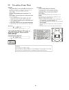
Some semiconductor (solid state) devices can be damaged easily by static electricity. Such components commonly are called Elec-
trostatic Sensitive (ES) Devices. Examples of typical ES devices are integrated circuits and some field-effect transistors and semi-
conductor "chip" components. The following techniques should be used to help reduce the incidence of component damage
caused by electrostatic discharge (ESD).
1. Immediately before handling any semiconductor component or semiconductor-equipped assembly, drain off any ESD on your
body by touching a known earth ground. Alternatively, obtain and wear a commercially available discharging ESD wrist strap,
which should be removed for potential shock reasons prior to applying power to the unit under test.
2. After removing an electrical assembly equipped with ES devices, place the assembly on a conductive surface such as alumi-
num foil, to prevent electrostatic charge buildup or exposure of the assembly.
3. Use only a grounded-tip soldering iron to solder or unsolder ES devices.
4. Use only an anti-static solder removal device. Some solder removal devices not classified as "anti-static (ESD protected)" can
generate electrical charge sufficient to damage ES devices.
5. Do not use freon-propelled chemicals. These can generate electrical charges sufficient to damage ES devices.
6. Do not remove a replacement ES device from its protective package until immediately before you are ready to install it. (Most
replacement ES devices are packaged with leads electrically shorted together by conductive foam, aluminum foil or compara-
ble conductive material).
7. Immediately before removing the protective material from the leads of a replacement ES device, touch the protective material
to the chassis or circuit assembly into which the device will be installed.
Caution
Be sure no power is applied to the chassis or circuit, and observe all other safety precautions.
8. Minimize bodily motions when handling unpackaged replacement ES devices. (Otherwise harmless motion such as the
brushing together of your clothes fabric or the lifting of your foot from a carpeted floor can generate static electricity sufficient
to damage an ES device).
Summary of DMP-BDT220GA
Page 1
Panasonic corporation © 2012. Unauthorized copying and distribution is a violation of law. Order no.Chm1203004ce blu-ray disc player model no. Dmp-bdt220ga dmp-bdt220gc dmp-bdt220gn dmp-bdt220gw dmp-bdt220gt dmp-bdt220pu dmp-bdt220px colour (k).......................Black type.
Page 2
2.
Page 3
3.
Page 4: Table of Contents
4 table of contents page page 1 safety precautions -----------------------------------------------5 1.1. General guidelines -----------------------------------------5 1.2. Caution for fuse replacement ---------------------------5 1.3. Caution for ac cord (only for bdt220gc)----------7 2 warning ----...
Page 5: 1 Safety Precautions
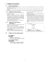
5 1 safety precautions 1.1. General guidelines 1. When servicing, observe the original lead dress. If a short circuit is found, replace all parts which have been overheated or damaged by the short circuit. 2. After servicing, see to it that all the protective devices such as insulation barriers, ins...
Page 6
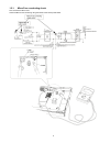
6 1.2.1. Micro fuse conducting check this unit uses the micro fuse. Check the micro fuse conducting using the tester at the check points below..
Page 7
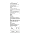
7 1.3. Caution for ac cord (only for bdt220gc).
Page 8: 2 Warning
8 2 warning 2.1. Prevention of electrostatic discharge (esd) to electrostatic sensitive (es) devices some semiconductor (solid state) devices can be damaged easily by static electricity. Such components commonly are called elec- trostatic sensitive (es) devices. Examples of typical es devices are in...
Page 9
9 2.2. Precaution of laser diode.
Page 10
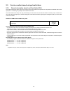
10 2.3. Service caution based on legal restrictions 2.3.1. General description about lead free solder (pbf) the lead free solder has been used in the mounting process of all electrical components on the printed circuit boards used for this equipment in considering the globally environmental conserva...
Page 11: 3 Service Navigation
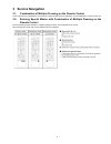
11 3 service navigation 3.1. Combination of multiple pressing on the remote control press multi-buttons (in combination) on the remote control simultaneously for operations, such as initialization or service mode, etc. 3.2. Entering special modes with combination of multiple pressing on the remote c...
Page 12
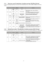
12 3.2.1. Disclosure mode (combination of multiple pressing: [ok] [blue] [yellow]) press and hold [ok] [blue] [yellow] on the remote control simultaneously for 5 sec., then "00 ret" is displayed on fl display window. 3.2.2. Nondisclosure mode 1 (combination of multiple pressing: [6] [7] [yellow]) pr...
Page 13
13 3.2.3. Nondisclosure mode 2 (combination of multiple pressing: [5] [9] [red]) press and hold [5] [9] [red] on the remote control simultaneously for about 5 sec., then "70 ret" is displayed on fl display window..
Page 14: 4 Specifications
14 4 specifications power supply: ac220-240v, 50/60hz (bdt220ga/gc/gw) ac220-240v, 50hz (bdt220gn) ac110v, 60hz (bdt220gt) ac110-240v, 50/60hz (bdt220pu/px) power consumption: approx. 9.9w (bdt220ga/gc/gn/gw/pu/px) approx.8.9w (bdt220gt) in standby mode: approx. 0.1w (bdt220ga/gc/gn/gw/gt) approx. 0...
Page 15
15 format: fat12, fat16, fat32, ntfs, mp3, jpeg, mpo,mkv, divx(bdt220ga/gc/gn/gw/gt/ pu), mp4, mpeg, wav, flac contents: jpeg: sd card, cd-r/rw, bd-re, dvd-r, usb device: pixcels: 34x34~8192x8192 sub sampling: 4:2:2, 4:2:0 motion jpeg not supproted sd card: jpeg conforming dcf(design rule for camera...
Page 16
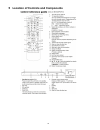
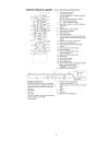
16 5 location of controls and components.
Page 17
17.
Page 18: 6 Operating Instructions
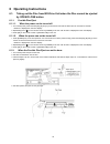
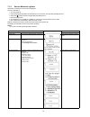
18 6 operating instructions 6.1. Taking out the disc from bd-drive unit when the disc cannot be ejected by open/close button 6.1.1. Forcible disc eject 6.1.1.1. When the power can be turned off. 1. Turn off the power, press and hold [ok], [b] and [y] on the remote control at the same time for more t...
Page 19: 7 Service Mode
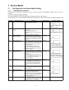
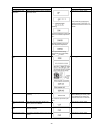
19 7 service mode 7.1. Self-diagnosis and special mode setting 7.1.1. Self-diagnosis functions self-diagnosis function provides information for errors to service personnel by “self-diagnosis display” when any error has occurred. U** and f** are stored in memory and held. You can check latest error c...
Page 20
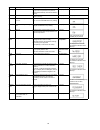
20 f34 initialization error when initialization error is detected after start- ing up main microprocessor, the power is turned off automatically. The event is saved in memory. No display no display f58 drive hardware error when drive unit error is detected, the event is saved in memory. No display n...
Page 21
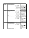
21 7.1.2. Special modes setting item fl display key operation mode name description rating password the audiovisual level setting password is initialized to level 8. While the unit is on, press and hold [ok], [b] and [y] on the remote control at the same time for more than 5 seconds. - "00 ret" is d...
Page 22
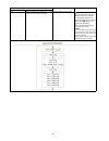
22 aging perform sequence of modes as * aging description shown below continually. Display following the then mode. Turn the power on. Press the [5] [9] and [r] button simultaneously for five seconds, then [70 ret] is displayed on fl. Press the [ ] button to select until [81 aig] is displayed on fl....
Page 23
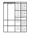
23 demonstration lock/unlock ejection of the disc is prohibited. The lock setting is effective until unlocking the tray and not released by main unit initialization of service mode. *when lock the tray. “lock” is displayed for 3 seconds. When the power is on, disc is in tray, press and hold [ok], [b...
Page 24
24 7.1.3. Service modes at a glance information necessary for service can be displayed. Service mode setting: 1. Turn the power off. 2. Press the [5] [9] and [r] button simultaneously for five seconds, then [70 ret] is displayed on fl. 3. Press the [ ] button to select until [80 srv] is displayed on...
Page 25
25 drive application check checking whether the drive is applicable drive or not. Press [0] [3] in service mode. Drive check simple quality of bd drive *if the date of the present or the trouble occurred time is incorrect, it may be not able to judge correctly. Press [3] [8] in service mode. Laser u...
Page 26
26 bd drive last error bd drive error code display. 1. Error number is displayed for 5 seconds. 2. Time when the error has occurred is display for 5 seconds. Yy: year mm: month dd: date 3. Last drive error (1/2) is displayed for 5 seconds. 00 : bad disc 03 : bad disc 04 : bad disc or drive malfuncti...
Page 27
27 6. Disc maker id is displayed for 5 seconds. In case that the maker cannot be identified, display is blackout. Item fl display key operation mode name description (remote controller key).
Page 28
28 7. Factor of drive error (hexadeci- mal) occurring is left displayed. 8. When the last error doesn't exist . Cec (h) output check check of the cec terminal high output of hdmi. Press [5] [5] in service mode. Cec (l) output check check of the cec terminal low output of hdmi. Press [5] [6] in servi...
Page 29
29 drive adjustment value initialization initialize the drive going to factory production adjustment values. Initializing: successful adjustment value initial- ization and automatic adjustment time : failed at initialization and auto- matic adjustment adjustment : when you enter the wrong password s...
Page 30
30 initialization of error code last error code information stored by timer is deleted. (write in f00) press [9] [8] in service mode. Initialization of the service mode last drive error, error history and error code information stored on the unit are initialized to factory setting. Press [9] [9] in ...
Page 31: 8 Service Fixture & Tools
31 8 service fixture & tools * the above parts are supplied by avc-csc-spc. Part number description pcs compatibility rfkz0216 extension cable (digital p.C.B. - power p.C.B. / 23 pin) 1 same as bd60 series rfkz0327 extension cable (digital p.C.B. - sd p.C.B. / 15 pin) 1 same as xw350 series rfkz03d0...
Page 32
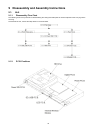
32 9 disassembly and assembly instructions 9.1. Unit 9.1.1. Disassembly flow chart the following chart is the procedure for disassembling the casing and inside parts for internal inspection when carrying out the servicing. To assemble the unit, reverse the steps shown in the chart below. 9.1.2. P.C....
Page 33
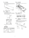
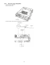
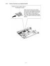
33 9.1.3. Top case 1. Remove the 3 screws . 2. Slide top case rearward and open the both ends at rear side of the top case a little and lift the top case in the direction of the arrows. 9.1.4. Front panel ass'y 9.1.4.1. Tray top 1. Put deck so that bottom can be seen. 2. Insert the paper clip, etc. ...
Page 34
34 9.1.4.5. How to assemble door ass'y. 1. Lean the right side of the door shaft against the side of relevant holes of the front panel, and insert the door shaft into the hole of the front panel. 2. Move the door leftward, and insert the 4 shafts of the front panel into the shaft hole of the door. 3...
Page 35
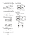
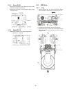
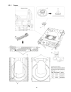
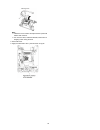
35 9.1.8. Power p.C.B. 1. Remove the connector (a) and screw (b) to remove the internal wireless module. 2. Remove the connector (c) and 3 screws (b) to remove the power p.C.B.. 9.1.9. Digital p.C.B. 1. Remove the 2 screws (a) to remove digital p.C.B.. 9.2. Bd drive 9.2.1. Tray 1. Insert the paper c...
Page 36
36 notes when attaching the tray: 1. Push slide cam to the left side slightly, and make sure the tray band is between the two posts of slide cam when attaching the tray. 9.2.2. Pulley gear, belt 1. Perform the step “ tray ”. 2. Push the post to the direction of arrow by using the slotted screwdriver...
Page 37
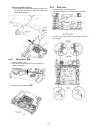
37 4. Slide the slid cam in the direction as shown, and then take the front post out of the slide cam track. 5. Take the damper out of the mecha chassis and remove the drive ass’ y. 6. Remove the slide cam..
Page 38
38 9.2.4. Drive gear and loading motor 1. Perform the step “ slide cam ”. 2. Remove the drive gear. 3. Loosen the hooks, and remove the loading motor unit and the sw ass'y..
Page 39
39 9.2.5. Grease.
Page 40
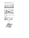
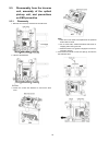
40 9.3. Disassembly from the traverse unit, assembly of the optical pick-up unit, and precautions on esd-preventive 9.3.1. Disassemly 1. Remove the connector, and take out the opu ffc. 2. Remove the mid base. 3. Loosen the 4 tabs with tweezers to remove the drive cover. Note: a. New drive cover need...
Page 41
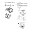
41 note: in this action, finger stab needs to be put on. Do not touch any parts other than the positions marked in the figure . 9.3.2. Assembly 1. Insert the shaft into the shaft hole of the base, install the opu to the auxiliary shaft, and then attach the nut piece unit onto the screw stem. 2. Asse...
Page 42
42 note: a. New drive cover needs to be replaced for the parts will deform after removal. B. Do not touch opu, shaft/countershaft, shaft motor or stepping motor during removal. 4. Insert opu ffc. 5. Apply the lubricants to the 1 point as shown in figure..
Page 43
43 9.3.3. How to clean the lens of optical pick-up.
Page 44
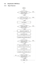
44 9.4. Adjustment of bd drive 9.4.1. Repair flowchart.
Page 45
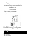
45 9.4.2. Adjustment 9.4.2.1. [drive] input opu-qr code(72) 1. Input 72 with the remote control's numeral keys in the service mode. The fl tube display “dqr__”(__ is blank) at this time. Qrcode scroll display is in the input state. 2. Input qrcode with remote control: the fl is displaying the input ...
Page 46
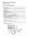
46 10 measurements and adjustments 10.1. Service positions note: for description of the disassembling procedure, see the section 9. 10.1.1. Checking and repairing of power p.C.B..
Page 47
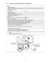
47 10.1.2. Checking and repairing of bd drive and digital p.C.B..
Page 48
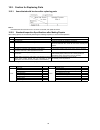
48 10.2. Caution for replacing parts 10.2.1. Items that should be done after replacing parts note 1: download latest firmware and burn it on cd-r or cd-rw, and update firmware. 10.2.2. Standard inspection specifications after making repairs after making repairs, we recommend performing the following...
Page 49
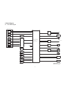
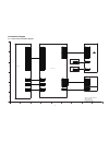
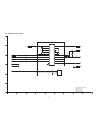
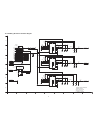
49 11 block diagram 11.1. Overall block diagram traverse mechanism unit optiacl pick-up unit usb port x51001 ic55004 ic55005 ic51001 servo controller/ av decoder/ system controller optical disc controller/ mixl ic54001 mixr overall block diagram key usb port p6803 fl led buzzer ic53002 laser diode m...
Page 50
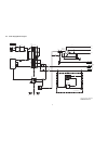
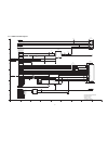
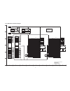
50 11.2. Power supply block diagram 1 2 3 4 2 5 4 5 n a 2 1 6 4 5 11 12 10 9 8 7 ac socket p1001 f1001 va1001,l1001 surge suppressor and surge absober d1006, c1014 rectifier t1001 power transformer ic1021 (switching ic) fb/olf vcc q1022 (feed back) d1110 (error voltage det.) fl_dcdc_on_h from/to dig...
Page 51
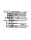
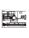
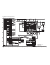
51 11.3. Digital p.C.B. Regulator block diagram digital p.C.B. Regulator block diagram 16,17,18 p58001 p1102 pw_x_sw5.9v from main p.C.B. (reg.Pw_dr5v) ic58302 vin vout pw_dr5v d5v a5v 5 1 2 cont (reg.5v) (reg.5v) 5v ic56302 vin vout 4 1 5 on hdmi_p_on_h ic51001- a13 from bp4 section from bp4 sectio...
Page 52
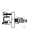
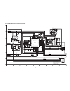
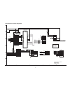
52 11.4. Digital (back end section) block diagram af22 ae22 usbdn1 usbdp1 usbdn1 usbdp1 21 22 26 29 28 ic59305 (usb controller) dm1 dp1 46 ccb1 45 ppb1 43 ppb2 dmu dpu 1 5 ic59303 vin vout /en /oc pw_usb1_5.1v ic51001 (bp4) 10m txc10 txd10 rxc10 rxd10 ic59020 ( ethernet controller) digital block dia...
Page 53
53 af11 mmck ae11 mmxck mmck_a mmxck_a l30 ck27xi l29 ck27xio x51001 (27mhz) ic51301 (8bit nand) ic52002 ic52001 ddr sdram 1gbit ddr sdram 1gbit 64m x 8bit nand flash memory 1 tc- bus_ed0-7_b 3 tc- mmdq0-15,mma0-13 2 tc- mmdq16-31,mma0-13 ddr3_i/f host i/f ic51001 (bp4) digital block diagram (back e...
Page 54
54 11.5. Ic pin terminal chart ic pin terminal chart ( tc 1 - tc 5) e m a n tr o p o n n i p o n n i p e m a n tr o p e m a n tr o p o n n i p o n n i p e m a n tr o p tc ic51001 / bp4 signal name ic52001 / sdram 1 tc ic51001 / bp4 signal name ic52001 / sdram 3 ic pin terminal chart c0dq0 c0dq1 c0dq...
Page 55
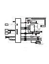
55 11.6. Digital (front end section) block diagram rfb rfa ina inb inc ind ine inf ing inh laser detector laser detector laser detector bd cd dvd fo/tr actuator spindle motor optical pick-up/traverse p55006 bd/dvd rf signal dvd focus and tracking signal bd focus and tracking signal cd main and sub s...
Page 56
56 11.7. Analog audio/video block diagram audio signal video signal ic51001 (bp4) (audio d/a converter) current segment dac analog mute aduio interface ic54001 ic56002 15 14 13 12 din m lrck g_dac_lrck g_dac_bck g_dac_dmix bck sck smpio30 smpio31 smpio32 c10 6 outl 7 outr g_dac_mck smpio33 b9 d10 k1...
Page 57
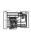
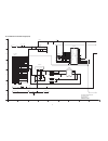
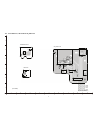
57 12 schematic diagram 12.1. Interconnection schematic diagram digital p.C.B. Bd drive power p.C.B. P55006 2 1 3 4 p1102 p58001 5 6 7 8 9 10 11 12 13 14 15 16 17 18 19 20 21 22 23 2 1 3 4 5 6 7 8 9 10 11 12 13 14 15 16 17 18 19 20 21 22 23 2 1 3 4 p1001 n a interconnection schematic diagram f e d 1...
Page 58
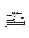
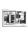
58 12.2. Power supply section schematic diagram power_p section f e d 1 c b a 9 8 7 6 5 4 3 2 schematic diagram 1 2 4 3 2 1 4 3 va1001 d4eay471a127 c1001 0.068 l1001 g0b233d00005 d1006 b0edkt000009 2 ! ! ! ! P1001 k2aa2b000011 f1001 k5g202y00006 t2al 250v ! C1005 470 1000p (bdt220pu/px/ga/gc/gn/gw) ...
Page 59
59 12.3. Fl section schematic diagram f e d 1 c b a 9 8 7 6 5 4 3 2 vss vdd sg1 sg2 sg3 sg4 sg5 sg6 sg7 sg8 sg9 vdd vss led2 led3 led4 osc dout din clk k1 stb sg16 sg17 sg18 f- f- p16 6g 5g 4g 3g 2g 1g p1 p2 p3 p4 p5 p6 p7 p8 p9 p10 p11 p12 p13 p14 p15 f+ f+ vee sg15 sg14 sg13 sg12 sg11 k2 34 35 36 ...
Page 60
60 12.4. Sd_usb section schematic diagram f e d 1 c b a 9 8 7 6 5 4 3 2 sd_usb section schematic diagram p6801 k1ky15aa0606 to p59301 digital p.C.B. Clk gnd 3 2 cmd 1 gnd dat3 6 5 dat2 4 dat1 dat0 9 8 3.3v 7 vbus cd 12 11 wp 10 fgnd dn 15 14 dp 13 ck6801 ck6802 ck6803 1 5 2 3 4 6 gnd p6803 k1fy104b0...
Page 61
61 12.5. Power sw and led section schematic diagram f e d 1 c b a 9 8 7 6 5 4 3 2 gnd 2 key_power 1 pj7551 vee1l10 to p7004 main p.C.B. Evq11a05r s7551 p7301 k1kb03b00007 main p.C.B. To p7001 1 2 3 led1 nc(gnd) vcc d7302 b3aea0000099 skype/standby r7302 220 power_sw section schematic diagram led sec...
Page 62
62 12.6. Audio schematic diagram f e d 1 c b a 9 8 7 6 5 4 3 2 audio section schematic diagram (digital p.C.B(1/7)) 20 19 18 17 16 15 14 13 7 6 5 4 3 2 1 8 ic54001 c1ab00003767 ldqq xsmt fmt din lrck avdd bck 12 sck 11 flt 9 agnd 10 demp cpgnd vcapp outl outr capm vneg dgnd cpvdd dcdd c54001 1 c5400...
Page 63
63 12.7. Video schematic diagram f e d 1 c b a 9 8 7 6 5 4 3 2 video section schematic diagram (digital p.C.B(2/7)) g_mixrout au g_mixlout agnd au dgnd dn svdac03 vout_mute_l bp au c56031 10 2 3 5 ic56002 c1ab00003363 vcc nc vout gnd ps vin 1 4 6 r56001 75 jk56002 k2ha2yyb0018 ar v al agnd dgnd htex...
Page 64
64 12.8. Ether_usb section schematic diagram(1/2) txen dvdd10 phyrstb mdc md1+[0] md1-[0] md1+[1] md1-[1] nc mdio intb gnd led0 led1 crs txer nc pmeb nc avdd33 gnd nc col rxer dvdd1out avdd33 ckxtal1 ckxtal2 nc rset nc gnd txc dvd33 rxc dvd33 rxd[0] rxd[1] rxd[2] rxd[3] 25 26 27 28 29 30 31 32 33 34...
Page 65
65 12.9. Ether_usb section schematic diagram(2/2) vssreg led4 led3 led2 led1 green amber vdd33 x1 x2 vdd25 vss dp4 dm4 vdd33 dm3 dp3 vdd25 dm2 dp2 vss dp1 b us_b test rref a vss(r) a vdd axss a vdd vdd33 dpu dmu vss vdd25 vb usm csb1 ppb1 csb2 ppb2 vss csb3 csb4 ppb3 ppb4 1 2 3 4 5 6 7 8 9 10 11 12 ...
Page 66
66 12.10. Digital_net section schematic diagram digital_net section (digital p.C.B.(4/7)) schematic diafram f e d 1 c b a 9 8 7 6 5 4 3 2 vin gnd cont 1 2 3 4 5 cn vo ic58302 c0dbgyy01974 c58089 10 c58143 0.22 c58090 10 tl58001 pw_dr5v fe c58088 10 cka11 cka10 cka9 cka6 cka4 cka1 cka5 cka3 cka2 cka8...
Page 67
67 12.11. Ddr3 section schematic diagram f e d 1 c b a 9 8 7 6 5 4 3 2 ddr3 section schematic diagram (digital p.C.B.(5/7)) ddr3 (#0) m3 ba2 n8 ba1 m2 ba0 t3 a13 n7 a12(/bc) r7 a11 l7 a10(ap) r3 a9 t8 a8 r2 a7 r8 a6 p2 a5 p8 a4 n2 a3 p3 a2 p7 a1 n3 a0 a3 dqu7 dqu6 dqu5 dqu4 dqu3 dqu2 dqu1 dqu0 b8 a2...
Page 68
68 12.12. Bp4 section schematic diagram(1/2) g7 vss vdd33 k6 vdd33 k10 vdd33 l10 vdd33 n17 vdd33 aa5 vdd33 k21 vdd33 aa20 vdd33 p17 avdd33_1abcvdac t4 avss_1abcvdac u2 avdd33_2vdac r5 avdd33_1dvdac t6 avss_1dvdac u4 avdd33vpll d6 avssvpll c6 t21 vss u15 vss u12 vss p12 vss p11 vss p10 vss ab19 vss a...
Page 69
69 12.13. Bp4 section schematic diagram(2/2) 17 16 15 14 f 13 12 11 10 9 e d c b a schematic diagram (digital p.C.B(6/7)) nc nc nc nc nc nc wp we ale nc nc io0 io1 io2 nc io3 c n e l c nc nc vss vcc nc nc nc nc vss vcc prl nc ce nc io4 ry/by gnd nc nc nc nc io5 io6 io7 nc nc re nc c n c n 1 2 3 4 5 ...
Page 70
70 12.14. Fe section schematic diagram(1/2) c55013 0.1 c55024 6.3v 220 f e d 1 c b a 9 8 7 6 5 4 3 2 fe section(1/2) (digital p.C.B.(7/7)) schematic diagram pw_dr5v dn lb55002 j0jjc0000005 l55001 g1c220ma0291 tl55005 cl55293 cl55296 4 1 c55034 22 p55006 k1my45a00001 to pick-up unit 10 11 15 16 17 18...
Page 71
71 12.15. Fe section schematic diagram(2/2) 1 2 3 4 p55001 k1mn04aa0046 a+ b- g_trvb- b+ a- g_trva+ g_trva- g_trvb+ trayload ldend 1 load_n tlt_p tlt_n p5v_1 fcs_p fcs_n load_p p5v12l trk_n trk_p pgnd_2 vtlt vfcs vtrk vload vspin vsled2 agnd_2 test5 test6 agnd_3 p5v_2 pgnd_1 c10v vsled1 p12v_1 gc xm...
Page 72
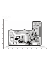
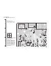
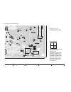
72 13 printed circuit board 13.1. Power p.C.B. Bdt220ga/gc/gn/gw p1001 f1001 va1001 c1001 l1001 w1 c1007 r1006 r1007 r1030 d1022 c1024 ip1021 r1032 d1021 d1023 r1022 q1022 r1111 r1112 r1113 ic1103 r1115 c1114 c1124 r1117 r7401 r1119 r1121 r1116 bz7401 q7401 r7404 r7410 q7402 r7407 r7409 qr7401 w10 c...
Page 73
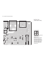
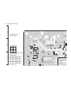
73 p7004 1 3 lb7002 w22 p7001 ir7001 3 1 31 w23 lb7001 za1005 mk1 w24 w8 c7006 qr7003 ckaa4 w14 ckaa5 ckaa6 d1112 w13 w3 c14303 c14306 q14301 r14306 d14301 l14302 r14305 4 3 6 1 w21 l1103 claa1 w15 ckaa3 r7009 r1172 ckaa2 c1172 r1176 mk2 q1170 d1171 q1171 r1173 c1175 t1101 1 9 r1174 d1175 d1172 d117...
Page 74
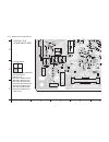
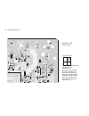
74 13.2. Power sw p.C.B., led p.C.B.And sd_usb p.C.B. Pj7551 p6803 ckk6803 ckk6802 ck6802 ckj6809 r6809 r6802 r6801 ckj6801 r6803 r6804 r6805 w101 lb6802 r6811 ck6803 p6801 2 1 14 ck6801 15 zj6801 3 1 w102 ckj6803 ckj6802 ckj6804 ckj6807 ckj6808 r6807 r6808 ckj6806 zj6802 31 w103 r6806 p6802 ckj6805...
Page 75
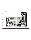
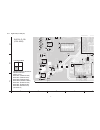
75 13.3. Digital p.C.B. 13.3.1. Digital p.C.B. (component side) (1/4) ic53002 tl55001 p55001 c55076 cl55294 c55053 c55054 c55055 lb55001 ip55004 r55084 cl55295 r55086 c55084 c55056 r55021 r55023 r55216 ic55006 5 1 cl55032 c55086 ckb27 1 c55190 cl55167 c551 15 c55070 mk12 24 13 c53019 mk8 jk56301 q56...
Page 76
76 13.3.2. Digital p.C.B. (component side) (2/4) jk59001 p59302 4 1 6 5 7 1 8 2 rl59009 rx59006 ic59020 24 13 37 48 c59003 r59015 rl59007 lb51019 lb51020 c51073 r52002 c51008 c51049 c51031 r52001 c51034 rl59010 rl5901 1 c51023 lb51016 c51068 c51069 r51024 c51053 rl59005 c52006 c52004 r52007 r52008 c...
Page 77
77 13.3.3. Digital p.C.B. (component side) (3/4) p55006 45 cl55166 r55003 cl55164 c55012 c55202 ckb25 c55151 rl55005 cl55075 cl55074 rl55004 c55187 cl55005 cl55006 c55033 l55001 c55024 c55035 c55050 p55007 5 c55052 c55034 lb55002 cl55293 c55013 tl55005 tl55004 rx55004 rx55005 rl55104 c55087 cl57301 ...
Page 78
78 13.3.4. Digital p.C.B. (component side) (4/4) c51034 lb51009 c51035 c51032 r52003 c51033 c51017 c51076 c59601 cl51207 lb59605 rx59601 lb51022 c51082 rx59303 r51026 rx51315 cl51202 cl51203 cl51204 cl51205 rx51306 mk2 c51081 c51075 lb51021 c51030 c51039 c51037 c52017 c52019 c52020 c52030 r52014 r52...
Page 79
79 13.3.5. Digital p.C.B. (foil side) (1/4) a b c ck5931 1 rx59305 ic59307 5 8 4 1 c59331 ic59306 c59335 c59336 r59365 r59360 r58053 r58049 r58052 c58015 ic58003 c58023 r58036 r58102 c58101 cka13 cka10 mk20 r52015 r52009 c52038 c58024 1 4 8 5 c58016 cka23 cka21 g58003 cka17 r58101 r59361 1 3 5 4 ck5...
Page 80
80 13.3.6. Digital p.C.B. (foil side) (2/4) ck56008 g56001 cks19 cks18 ck56002 r56001 c56343 lb56002 c56031 ic56302 3 1 4 5 c56342 ic56002 r56013 ck54121 ck54122 ck54124 r56302 cl57021 rx55010 mk17 c55063 c55067 c55068 c55066 rl55039 cl55040 rx55015 cl55093 cl55092 cl55091 c55083 ic55004 56 29 12 8 ...
Page 81
81 13.3.7. Digital p.C.B. (foil side) (3/4) 5 4 3 2 1 e d f cka10 c58075 c58077 mk20 r52015 c52040 r52013 c52024 lb59304 t59304 t59301 4 3 1 2 3 4 2 1 mk24 1 24 48 25 c59308 c59307 c59312 c5931 1 c58071 ic58004 r58030 c58078 ic58005 r58031 c58036 c58050 r58019 r58024 ic59302 5 8 4 1 r59366 r59362 r5...
Page 82
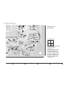
82 13.3.8. Digital p.C.B. (foil side) (4/4) 9 8 7 6 5 c55355 ic55300 41 58 rl51103 cl57122 cl57118 cl57119 cl57202 cl55036 c55406 rx57005 cl57151 cl55031 cl57125 rl55023 cl57124 rx51313 cl55152 rl55155 rl55158 rl55157 rl55156 cl57002 cl57117 cl57030 rx55016 r57001 c57014 cl57116 cl57201 c551 13 mk23...
Page 83
83 13.3.9. Digital p.C.B. Address information transistors digital p.C.B. Transistor-resistors address information c......Component side f......Foil side integrated circuits ip protectors test points connectors qr59301 f-7 c q56301 b-3 c ip55004 b-3 c ic51001 d-5 f ic51301 e-5 f ic52001 c-4 f ic52002...
Page 84
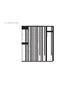
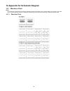
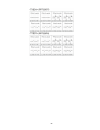
84 14 appendix for schematic diagram 14.1. Waveform chart note: circuit waveform described herein shall be regarded as reference information when probing defect point, because it may differ from an actual measuring value due to difference of measuring instrument and its measuring condition and produ...
Page 85
85.
Page 86
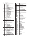
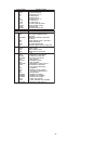
86 14.1.2. Abbreviations initial/logo abbreviations a a0~up aclk ad0~up adata ale amute areq arf asi aso async address audio clock address bus audio pes packet data address latch enable audio mute audio pes packet request audio rf servo amp inverted input servo amp output audio word distinction sync...
Page 87
87 initial/logo abbreviations t te tibal tid tin tip tis tpsn tpso tpsp trcrs tron trson tracking error balance control balance output 1 balance input balance input balance output 2 op amp input op amp output op amp inverted input track cross signal tracking on traverse servo on initial/logo abbrevi...
Page 88
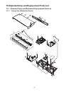
88 15 exploded view and replacement parts list 15.1. Exploded views and mechanical replacement parts list 15.1.1. Casing parts & mechanism section 21 42 43 11 41 20 1 37 35 36 3 33 9 2 12 32 31 20-1 20-2 20-2-1 20-2-2 20-2-3 19 17 18 16 39 38 15 40 34 45 46 47 44 48 5 8 14 20-3 49 6 7 13.
Page 89
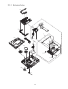
89 15.1.2. Mechanism section 102 110 103 111 105 108 107 112 109 122 106 104 117 123 121 118 123-2 123-3 123-4 123-5 123-6 120 119 123-1 101 123-9 123-10 123-8 123-7.
Page 90
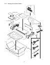
90 15.1.3. Packing & accessories section a6 pc4 pc3 pc2 pc5 a4 a4-1 pc1 a7 a10 (bdt220pu/px) (bdt220ga/gc/gw/pu/px) (bdt220gt) (bdt220gc) (bdt220gn) a1 (bdt220ga/gc/gw/pu) a2 a3 (bdt220gn/gt) a16(bdt220gt) pc7 (bdt220gc).
Page 91
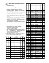
91 15.1.4. Mechanical replacement parts list notes: *important safety notice: components identified by mark have special character- istics important for safety. Furthermore, special parts which have purposes of fire-retardant (resistors), high-quality sound (capacitors), low-noise (resistors), etc. ...
Page 92
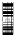
92 110 vmd6549 mecha chassis 1 111 vmd6550 slide cam 1 112 vmg1720 belt 1 117 vwj2303 opu ffc 1 118 vhd2377 nut piece screw 1 119 vmb4004-j nut piece spring 1 120 vmd6551 nut piece 1 121 raf3620a-c opu 1 adj 122 vxa8986 sw ass'y 1 123 vxa8971-ser traverse unit(without opu) 1 123-1 l6kayyyh0008 stepp...
Page 93
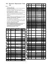
93 15.2. Electrical replacement parts list notes: *important safety notice: components identified by mark have special character- istics important for safety. Furthermore, special parts which have purposes of fire-retardant (resistors), high-quality sound (capacitors), low-noise (resistors), etc. Ar...
Page 94
94 l1103 g0c100ka0174 coil 1 bdt220ga /gc/gn/ gt/gw l1105 g0c100ka0174 coil 1 bdt220ga /gc/gn/ gt/gw l14302 g0a100za0045 coil 1 bdt220pu /px lb1018 j0jhc0000048 coil 1 bdt220pu /px/ga/ gc/gn/gw lb1018 erj6gey0r00v coil 1 bdt220gt lb14301 j0jhc0000048 coil 1 bdt220pu /px p1001 k2aa2b000011 ac inlet 1...
Page 95
95 s7551 evq11a05r switch(power) 1 vep70494a led p.C.B. (rtl) e.S.D. D7302 b3aea0000099 diode 1 e.S.D. R7302 erj6geyj221v 1/10w 220 1 p7301 k1kb03b00007 connector(3p) 1 rfkb76272eat digital p.C.B. E.S.D. Adj bdt220ga rfkb76272ht digital p.C.B. E.S.D. Adj bdt220gc rfkb76272gt digital p.C.B. E.S.D. Ad...
Page 96
96 c55066 f1g1a104a012 10v 0.1u 1 c55067 f1j1e104a137 25v 0.1u 1 c55068 f1g0j1050007 6.3v 1u 1 c55070 f1g1c104a077 16v 0.1u 1 c55071 f1g1c104a077 16v 0.1u 1 c55076 f1j1c475a059 16v 4.7u 1 c55083 f1g1c104a077 16v 0.1u 1 c55084 f1j1c106a059 16v 10u 1 c55086 f1h0j4750004 6.3v 4.7u 1 c55087 f1g1e222a086...
Page 97
97 ic51301 rfkb76272bt digital p.C.B. 1 e.S.D. Adj bdt220pu ic51301 rfkb76272ax digital p.C.B. 1 e.S.D. Adj bdt220px ic52001 c3abuy000007 ic 1 e.S.D. Ic52002 c3abuy000007 ic 1 e.S.D. Ic53002 b3zaz0000022 ic 1 e.S.D. Ic54001 c1ab00003767 ic 1 e.S.D. Ic55004 c0gby0000118 ic 1 e.S.D. Ic55005 c0gby00000...
Page 98
98 r58019 erj2rhd223x 1/16w 22k 1 r58020 erj2rhd223x 1/16w 22k 1 r58024 erj2rhd222x 1/16w 2.2k 1 r58030 erj2rhd223x 1/16w 22k 1 r58031 erj2rhd123x 1/16w 12k 1 r58036 erj3geyj100v 1/20w 10 1 r58049 erj2rhd683x 1/16w 68k 1 r58052 erj2rhd472x 1/16w 4.7k 1 r58053 erj2rhd223x 1/16w 22k 1 r58101 erj2gej10...
Page 99
99 16 schematic diagram for printing with a4 size.

