- DL manuals
- Panasonic
- Telephone
- KX-TC1868B
- Service Manual
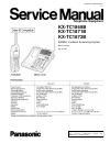
Panasonic KX-TC1868B Service Manual - 2 Location Of Controls
Summary of KX-TC1868B
Page 1
© 2000 kyushu matsushita electric co., ltd. All rights reserved. Unauthorized copying and distribution is a violation of law. Kx-tc1868b kx-tc1871b kx-tc1872b 900mhz cordless answering system black version (for u.S.A.) telephone equipment order no. Km40008667c1 f11.
Page 2: Contents
1 standard battery life 3 2 location of controls 4 3 displays 5 4 connection 8 5 operation 10 6 disassembly instructions 18 7 assembly instructions 20 8 troubleshooting guide 22 9 test mode and adjustment 36 10 description 40 11 terminal guide of ic´s, transistors and diodes 44 12 block diagram (bas...
Page 3: 1 Standard Battery Life
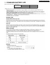
After your panasonic battery is fully charged; * within about 10 feet (3 m) 1 standard battery life while in use (talk) near the base unit* up to about 6 hours away from the base unit up to about 4 hours while not in use (stand-by) up to about 14 days 3 kx-tc1868b / kx-tc1871b / kx-tc1872b.
Page 4: 2 Location Of Controls
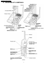
2 location of controls (base unit) (handset) 4 kx-tc1868b / kx-tc1871b / kx-tc1872b.
Page 5: 3 Displays
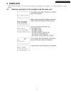
3 displays both the handset and the base unit show you instructions and information on the displays. These display prompts are shown below. 3.1. Common prompts for the handset and the base unit 5 kx-tc1868b / kx-tc1871b / kx-tc1872b.
Page 6
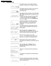
3.2. Handset only 6 kx-tc1868b / kx-tc1871b / kx-tc1872b.
Page 7
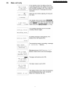
3.3. Base unit only 7 kx-tc1868b / kx-tc1871b / kx-tc1872b.
Page 8: 4 Connection
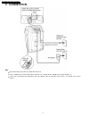
4 connection note: • use only with panasonic ac adaptor pqlv1z. • the ac adaptor must remain connected at all times. (it is normal for the adaptor to feel warm during use.) • if your unit is connected to a pbx which does not support caller id and voice mail services, you cannot access those services...
Page 9
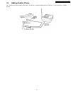
4.1. Adding another phone this unit will not function during a power failure. To connect a standard telephone on the same line, use the panasonic t-adaptor kx-j66. 9 kx-tc1868b / kx-tc1871b / kx-tc1872b.
Page 10: 5 Operation
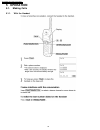
5.1. Making calls 5 operation 5.1.1. With the handset 10 kx-tc1868b / kx-tc1871b / kx-tc1872b.
Page 11
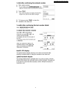
11 kx-tc1868b / kx-tc1871b / kx-tc1872b.
Page 12
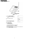
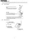
5.1.2. With the base unit 12 kx-tc1868b / kx-tc1871b / kx-tc1872b.
Page 13
13 kx-tc1868b / kx-tc1871b / kx-tc1872b.
Page 14
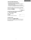
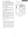
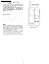
5.2. Answering calls 5.2.1. With the handset when a call is received, the unit rings and the caller id button on the base unit flashes quickly. If you subscribe to a caller id service, the calling party information will be displayed after the first ring. In order to view the caller id information, p...
Page 15
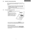
5.3.1. Setting the unit to answer calls 5.3. Automatic answering operation 15 kx-tc1868b / kx-tc1871b / kx-tc1872b.
Page 16
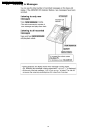
5.4. Listening to messages 16 kx-tc1868b / kx-tc1871b / kx-tc1872b.
Page 17
5.4.1. During playback 17 kx-tc1868b / kx-tc1871b / kx-tc1872b.
Page 18: 6 Disassembly Instructions
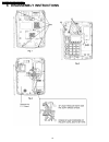
6 disassembly instructions 18 kx-tc1868b / kx-tc1871b / kx-tc1872b.
Page 19
Shown in fig.- to remove remove 1 lower cabinet screws (2.6 x 12).....(a) x 5 2 main p.C. Board remove the p.C. Board 3 lower cabinet screw (3 x 12).....(b) x 1 screws (3 x 8).....(c) x 3 4 battery cover remove the battery cover 5 rear cabinet screws (2.6 x 12).....(d) x 2 screw (2.6 x 12).....(e) x...
Page 20: 7 Assembly Instructions
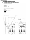
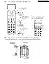
7 assembly instructions 7.1. Asseembly the lcd to p.C. Board (base unit) 20 kx-tc1868b / kx-tc1871b / kx-tc1872b.
Page 21
7.2. Asseembly the lcd to p.C. Board (handset) 7.3. Adjustment to prevent the cabinet from opening at dropping stick the rubber on the front cabinet as shown in the figure to prevent the cabinet from opening at dropping. 21 kx-tc1868b / kx-tc1871b / kx-tc1872b.
Page 22: 8 Troubleshooting Guide
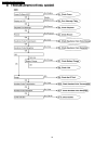
8 troubleshooting guide 22 kx-tc1868b / kx-tc1871b / kx-tc1872b.
Page 23
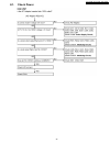
8.1. Check power 23 kx-tc1868b / kx-tc1871b / kx-tc1872b.
Page 24
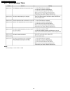
8.2. Error message table note: flash memory is ic751. Dsp is ic501 24 kx-tc1868b / kx-tc1871b / kx-tc1872b.
Page 25
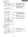
8.4. Check playback 8.3. Check record 25 kx-tc1868b / kx-tc1871b / kx-tc1872b.
Page 26
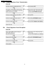
8.5. Check sp-phone voice transmission 8.6. Check sp-phone voice reception 26 kx-tc1868b / kx-tc1871b / kx-tc1872b.
Page 27
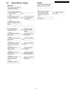
8.7. Check battery charge 27 kx-tc1868b / kx-tc1871b / kx-tc1872b.
Page 28
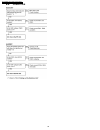
8.8. Check link 28 kx-tc1868b / kx-tc1871b / kx-tc1872b.
Page 29
8.9. Check the rf unit 8.9.1. Finding out the defective unit prepare hs jig (handset-jig) and bs jig (base unit-jig). Place the hs jig on the cradle of the base unit for checking, then confirm that they are linked. Place the handset for checking on the cradle of the bs jig, then confirm that they ar...
Page 30
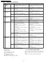
8.9.2.2. Base unit - jig (bs jig) for handset the base unit jig uses two modes: normal power mode and test power mode. These modes alternate when the base unit locator button is pressed: (1) normal power mode, test super low (red) is off. This test simulates the handset is at normal/close distance. ...
Page 31
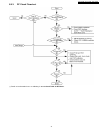
8.9.3. Rf check flowchart (*) details of confirmation items are following in “8.9.4. Check table for rf block”. 31 kx-tc1868b / kx-tc1871b / kx-tc1872b.
Page 32
(*1)bs;base unit, hs;handset unit, hs jig;handset-jig, bs jig;base unit-jig (*2)marconi setting tx freq.; 906.00mhz mode; wb spectrum analyzer setting freq. 906.00mhz span 10mhz rbw 1mhz or above vbw same as rbw (*3)see “9 test mode and adjustment” (*4)do not adjust x101 when probe is directly attac...
Page 33
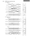
8.9.5. Rf-dsp interface signal wave form 33 kx-tc1868b / kx-tc1871b / kx-tc1872b.
Page 34
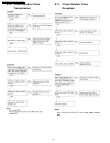
8.10. Check handset voice transmission 8.11. Check handset voice reception note: when checking the rf unit, refet to 8.9. Check the rf unit 34 kx-tc1868b / kx-tc1871b / kx-tc1872b.
Page 35
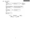
8.12. Check call id 35 kx-tc1868b / kx-tc1871b / kx-tc1872b.
Page 36
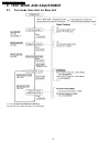
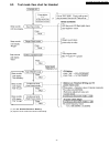
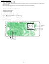
9 test mode and adjustment 9.1. Test mode flow chart for base unit (*1) see 9.4. Base unit reference drawing (*2) special check method for base unit individually. 36 kx-tc1868b / kx-tc1871b / kx-tc1872b.
Page 37
9.2. Test mode flow chart for handset (*1) see 9.5. Handset reference drawing (*2) special check method for handset individually. 37 kx-tc1868b / kx-tc1871b / kx-tc1872b.
Page 38
9.3. Adjustment x101 in case of ss system, carrier signal frequency directly by frequency counter, can not be measured because sending signal is spread by pn code. So, the confirmation and adjustment is made under the continuous send mode of test mode. Adjust the tx carrier(cw) frequency on the rf u...
Page 39
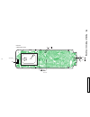
9.5. Handset reference drawing handset (component view) ant gnd 100 mic mic test pull up 10 10 ant vc101 sp sp + - + - 39 kx- tc186 8b / kx-tc 1871b / kx- tc187 2b.
Page 40: 10 Description
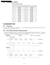
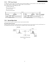
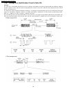
10 description 9.6. Frequency table 10.1. Frequency the frequency range of 906.00 mhz ~ 923.25 mhz is used. Transmitting and receiving channel between base unit and handset is same frequency. Refer to the frequency table. 10.2. Time division duplex (tdd) operation transmission/reception between the ...
Page 41
10.2.1. Tdd frame format the tdd frame is 2ms in length, and is composed of two symmetrical 960 µs tx and rx subframes. Each subframe contains 96 bits of 10µs duration, with 40µs guard times between both tx and rx subframes. Each subframe consists of the following four fields: • a 16-bit preamble fi...
Page 42
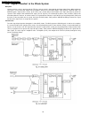
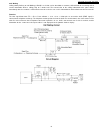
10.4. Signal flowchart in the whole system reception cn101 of the base unit is connected to the tel line, and the signal is input through the bridge diode d101. While talking the relay (q121) is turned on and amplified at the amplifiers q461, then led to dsp (ic501). Dsp generates adpcm signal. The ...
Page 43
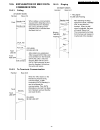
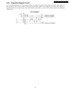
10.5. Explanation of bbic data communication 10.5.1. Calling 10.5.2. To terminate communication 10.5.3. Ringing 43 kx-tc1868b / kx-tc1871b / kx-tc1872b.
Page 44
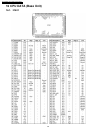
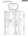
11 terminal guide of ic´s, transistors and diodes 11.1. Base unit 11.2. Handset 44 kx-tc1868b / kx-tc1871b / kx-tc1872b.
Page 45
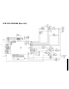
12 block diagram (base unit) kx -t c186 8b / k x -t c 1871b / k x -t c 187 2b 45.
Page 46
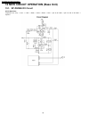
13 new circuit operation (base unit) 13.1. Sp-phone rx circuit circuit operation: telephone line (t/r) → q131 → c463 → r448 → c442 → r464 → c441 → pin 38 of ic501 → pins 32 and 33 of ic501 → speaker 46 kx-tc1868b / kx-tc1871b / kx-tc1872b.
Page 47
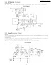
13.2. Sp-phone tx circuit circuit operation: mic → c724 → c725 → c726 → r726 → pin 47 of ic501 → pin 36 of ic501 → r431 → c432 → c433 → telephone line 13.3. Auto disconnect circuit function: this circuit is used to detect the fact that another telephone connected to the same line is off-hook while t...
Page 48
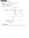
13.4. Power supply circuit function: power from the ac adaptor passes through a regulating block consisting of ic301. Circuit operation: ic401 is a regulated power supply. The voltage at point a is regulated to 4.5 v by ic301. The voltage at point b is dropped by d306 and d307 to 4.1 v. The voltage ...
Page 49
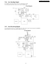
13.6. Line sending signal the modulation signal input from the rf unit is demodulated by ic501. The audio signal output from ic501-36 and is input to telephone line. 13.7. Line receiving signal the audio signal from line passes through q106 and ic702, and the signal is input to pin 96 of ic502(bbic)...
Page 50
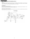
13.8. Calling line identification circuit (caller id) function: the caller id is a chargeable id which the user of a telephone circuit obtains by entering a contract with the telephone company to utilize a caller id service. For this reason, the operation of this circuit assumes that a caller id ser...
Page 51
L call waiting calling identity delivery on call waiting (cidcw) is a class service that allows a customer, while off-hook on an existing call, to receive information about a calling party on a waited call. The transmission of the calling information takes place almost immediately after the customer...
Page 52
13.9. Parallel connection detection circuit function: in order to disable call waiting and stutter tone functions when using telephones connected in parallel, it is necessary to have a circuit that judges whether a telephone connected in parallel is in use or not. This circuit determines whether the...
Page 53
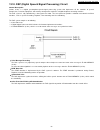
13.10. Dsp (digital speech/signal processing) circuit general description: (ic501, ic751) is a digital speakerphone/speech/signal processing system that implements all the functions of speech compression, record and playback, and memory management required in a digital telephone answering machine. T...
Page 54
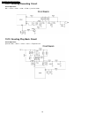
13.11. Greeting recording circuit circuit operation: mic → c724 → c725 → c726 → r726 → pin 47 of ic501. 13.12. Greeting play back circuit circuit operation: pin36 of ic501 → r431 → c432 → c433 → telephone line. 54 kx-tc1868b / kx-tc1871b / kx-tc1872b.
Page 55
13.13. Icm recording circuit circuit operation: telephone line → q131 → c463 → r448 → c442 → r464 → c441 → pin 32 and 33 of ic501. 13.14. Icm play circuit circuit operation: pins 32 and 33 of ic501 → speaker. 55 kx-tc1868b / kx-tc1871b / kx-tc1872b.
Page 56
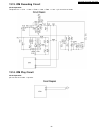
13.15. Telephone line interface circuit operation: l answer in the idle mode, q121 is open to cut the dc loop current and decrease the ring load. When ring voltage appears at the tip (t) and ring (r) leads (when the telephone rings), the ac ring voltage is transferred as follows: t → l101 → r103 → c...
Page 57
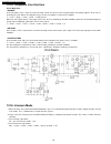
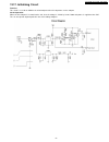
13.17. Initializing circuit function: this circuit is used for to initialize the microcomputer when it incorporates an ac adaptor. Circuit operation: when the ac adaptor is inserted into the unit, then the voltage is shifted by ic301, d306 and power is supplied to the dsp. The set can operate beyond...
Page 58
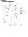
14 block diagram (handset) 58 kx-tc1868b / kx-tc1871b / kx-tc1872b.
Page 59
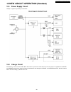
15 new circuit operation (handset) 15.1. Power supply circuit voltage is supplied separately to each block. 15.2. Charge circuit ni-cd battery is connected to cn202. When the handset is put on the cradle of the base unit, the power is supplied from charge1 and charge2 terminals to charge the battery...
Page 60
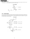
15.3. Ringer circuit if the ringer volume is set to low and an alarm tone is output from 39 pin, ic201 dsp and input to q209. Then q208 is turned off. If the ringer volume is set to high, q208 turns on and results in a louder beep tone. 15.4. Sending signal the voice signal from the microphone input...
Page 61
15.5. Reception signal circuit the received signal from the base unit is output from pins 33 (spn) and 32 (spp) of ic201 (dsp) as the voice signal. Spn is the inverse output of spp, and the speaker is driven by spn and spp. Cn203 is the headphone jack. When the headphone is connected to this jack, t...
Page 62: 16 Cpu Data (Base Unit)
16 cpu data (base unit) 16.1. Ic501 62 kx-tc1868b / kx-tc1871b / kx-tc1872b.
Page 63: 17 Cpu Data (Handset)
17 cpu data (handset) 17.1. Ic201 63 kx-tc1868b / kx-tc1871b / kx-tc1872b.
Page 64
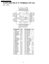
18 explanation of ic terminals (rf unit) 18.1. Ic101 64 kx-tc1868b / kx-tc1871b / kx-tc1872b.
Page 65: 19 How To Replace Flat
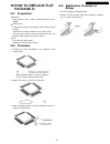
19 how to replace flat package ic 19.1. Preparation • solder sparkle solder 115a-1, 115b-1 or almit solder kr-19, kr- 19rma • soldering iron recommended power consumption will be between 30 w to 40 w. Temperature of copper rod 662 ± 50°f (350 ± 10°c) (an expert may handle between 60 w to 80 w iron, ...
Page 66
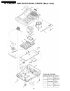
20 cabinet and electrical parts (base unit) 66 kx-tc1868b / kx-tc1871b / kx-tc1872b.
Page 67
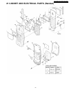
21 cabinet and electrical parts (handset) 67 kx-tc1868b / kx-tc1871b / kx-tc1872b.
Page 68
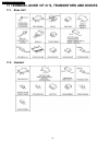
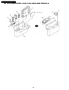
22 accessories and packing materials 68 kx-tc1868b / kx-tc1871b / kx-tc1872b.
Page 69: 23 Replacement Parts
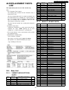
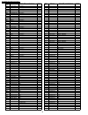
23 replacement parts list this replacement parts list are u.S.A. Version only. Note: 1. Rtl (retention time limited) the marking (rtl) indicates that the retention time is limited for this item. After the discontinuation of this assembly in production, the item will continue to be available for a sp...
Page 70
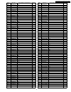
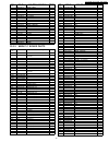
Ref. No. Part no. Part name & description remarks d121 pqvdrlz20a diode(si) d122 pqvdrlz2r0 diode(si) d302 pqvdrlz8r2 diode(si) d303 pqvdrlz8r2 diode(si) d306 pqvdhru0302a diode(si) d313 ma8047 diode(si) d315 pqvdhru0302a diode(si) d321 ma8051 diode(si) d331 ma8036h diode(si) d371 ma111 diode(si) d3...
Page 71
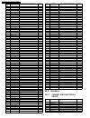
Ref. No. Part no. Part name & description remarks r344 erj3geyj104 100k r345 erj3geyj224 220k r371 erj3geyj121 120 r372 erj3geyj561 560 r373 erj3geyj220 22 r374 erj3geyj220 22 r375 erj3geyj220 22 r376 erj3geyj220 22 r377 erds1tj221 220 s r378 erds1tj221 220 s r381 erj3geyj563 56k r382 erj3geyj563 56...
Page 72
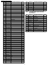
Ref. No. Part no. Part name & description remarks c442 ecuv1c104kbv 0.1 c443 ecuv1h101jcv 100p c444 ecuv1c104kbv 0.1 c445 ecst0jz106r 10 c461 ecuv1c104zfv 0.1 c463 ecuv1c104kbv 0.1 c464 ecuv1h470jcv 47p c466 ecuv1h101jcv 100p c467 ecuv1h470jcv 47p c470 ecst0jz106r 10 c501 ecea0ju102 1000 c502 ecuv1c...
Page 73
Ref. No. Part no. Part name & description remarks 6 pqhg10527y rubber sheet 7 pqhr10726z lcd holder 8 pqhr10727z lcd plate 9 pqhr10739z sp holder 10 pqhs10410y double side tape 11 pqhs10425z sp sponge 12 pqhx10862z lcd cover sheet 13 pqhx10955z lcd sheet 14 pqhx10959z cushion 15 pqjt10158z charge te...
Page 74
Ref. No. Part no. Part name & description remarks r245 erj3geyj103 10k r246 erj3geyj153 15k r247 erj3geyj391 390 r248 erj3geyj393 39k r249 erj3geyj222 2.2k r250 erj3geyj222 2.2k r251 erj3geyj120 12 r252 erj3geyj221 220 r253 erj3geyj222 2.2k r260 erj3geyj104 100k r263 erj3geyj104 100k r264 erj3geyj10...
Page 75: 24 For Schematic Diagram
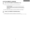
24 for schematic diagram 24.1. Base unit (28 schematic diagram (base unit)) notes: 1. Dc voltage measurements are taken with voltmeter from the negative voltage line. This schematic diagram may be modified at any time with the development of new technology. 24.2. Handset (30 schematic diagram (hands...
Page 76
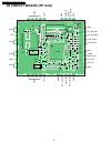
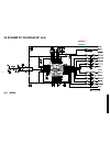
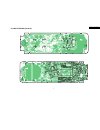
25 circuit board (rf unit) r120 c114 r103 c112 r102 l106 c1 l1 l2 c3 c2 c137 c109 c120 r104 r137 r136 r117 r111 r110 r109 r128 r108 c122 r135 c133 r115 r133 c130 r134 l105 c110 r101 l104 l102 c136 l103 c108 c119 x101 c111 gnd gnd tx_adpcmi rx_adpcmo pcm_sync pcm_bclk irq open (mcu clk) spi_ale spi_e...
Page 77
26 schematic diagram (rf unit) tx rx ic101 26.1. Memo kx -t c186 8b / k x -t c 1871b / k x -t c 187 2b 77.
Page 78
Kx-tc1868b / kx-tc1871b / kx-tc1872b 78.
Page 79
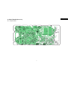
27 circuit board (base unit) 27.1. Component view rf unit cn101 b c e b c e e b b e c e b c c ant gnd ant la lb e c b e c b e c b b c e c381 c371 c773 c774 r771 r772 q381 r134 r371 r133 r381 r382 r140 r139 r432 r431 c704 r383 c431 c133 r132 d381 c432 c433 c798 j902 c551 c797 c927 c796 c795 c794 c793...
Page 80
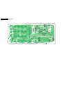
27.2. Flow solder side view kx-tc1868b / kx-tc1871b / kx-tc1872b 80
Page 81
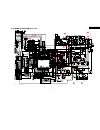
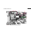
28 schematic diagram (base unit) ic331 ic301 sp phone tx sp phone rx talk tx talk rx -51dbm/600 Ω 1.1khz 4.2v 215mv 730mv 4.1v 4.5v 4.5v 4.2v 3.6v 10.5v 7.6v 10.5v 7.7v 7.4v 4.2v 960mvp-p 255mvp-p 760mvp-p 105mvp-p 175mvp-p 85mvp-p 22mvp-p 1000mvp-p output 140mvp-p (-25dbm/600 Ω ) input 1.1khz ic751...
Page 82
Kx-tc1868b / kx-tc1871b / kx- tc1872b 82.
Page 83
29 circuit board (handset) c294 ic201 ic202 ic204 ic205 ic203 kx-tc1868b / kx-tc1871b / kx-tc1872b 83.
Page 84
Kx-tc1868b / kx-tc1871b / kx- tc1872b 84.
Page 85
30 schematic diagram (handset) 130mvp-p 270mvp-p loud vol. Mid 3.3v 3.0v 140mvp-p 2.4v 490mvp-p 90mvp-p (headset) tx rx -43dbm/600 (headset) input 1.1khz input 1.1khz 18mvp-p (-45dbm/600 ) 0.45v 3.0v c294 0.01u 0.01u 120n 120n 10k 12k 0.056u * "nc" is the part not used. Ic201 ic202 ic204 ic203 ic205...
Page 86
Kx-tc1868b / kx-tc1871b / kx- tc1872b 86.
Page 87
87 kx-tc1868b / kx-tc1871b / kx-tc1872b m (w) kxtc1868b kxtc1871b kxtc1872b printed in japan.

