- DL manuals
- Panasonic
- Answering Machine
- KX-TG2359BXB
- Service Manual
Panasonic KX-TG2359BXB Service Manual - 10.2. Handset
Summary of KX-TG2359BXB
Page 1
© 2004 panasonic communications co., ltd. All rights reserved. Unauthorized copying and distribution is a violation of law. Kx-tg2359bxb dual handsets digital cordless answering system black version (for asia, middle near east and other areas) telephone equipment order no. Km40404398c3.
Page 2: Note:
1 about lead free solder (pbf: pb free) 4 1.1. Suggested pbf solder 4 1.2. How to recognize that pb free solder is used 5 2 for service technicians 7 3 caution 7 4 battery 8 4.1. Standard battery life 8 4.2. Battery replacement 9 5 location of controls 10 5.1. Base unit 10 5.2. Handset 11 5.3. Charg...
Page 3
17.1. Dsp (digital speech/signal processing: ic501) 76 17.2. Flash memory (ic701) 77 17.3. Power supply circuit 77 17.4. Reset circuit 79 17.5. Locator/intercom mode 80 17.6. Telephone line interface 80 17.7. Auto disconnect circuit 81 17.8. Parallel connection detect circuit 82 17.9. Calling line i...
Page 4: 1.1. Suggested Pbf Solder
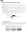
1 about lead free solder (pbf: pb free) note: in the information below, pb, the symbol for lead in the periodic table of elements, will refer to standard solder or solder that contains lead. We will use pbf solder when discussing the lead free solder used in our manufacturing process which is made f...
Page 5
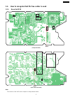
1.2. How to recognize that pb free solder is used 1.2.1. Base unit pcb ic201 ic501 ic300 ic701 ic901 ic601 pbf marked (component view) ic301 pbf lcd700 marked (flow solder side view) note: the location of the “pbf” mark is subject to change without notice. 5 kx-tg2359bxb.
Page 6: Pbf
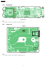
1.2.2. Handset pcb ic901 ic204 ic201 ic202 ic203 pbf marked (component view) note: the location of the “pbf” mark is subject to change without notice. 1.2.3. Charger unit ic1 pbf cn1 marked (component view) note: the location of the “pbf” mark is subject to change without notice. 6 kx-tg2359bxb.
Page 7: 2 For Service Technicians
2 for service technicians ics and lsis are vulnerable to static electricity. When repairing, the following precautions will help prevent recurring malfunctions. 1. Cover plastic parts boxes with aluminum foil. 2. Ground the soldering irons. 3. Use a conductive mat on worktable. 4. Do not grasp ic or...
Page 8: 4 Battery
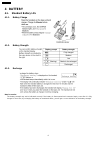
4 battery 4.1. Standard battery life 4.1.1. Battery charge 4.1.2. Battery strength 4.1.3. Recharge note for service: the battery strength may not be indicated correctly if the battery is disconnected and connected again, even after it is fully charged. In that case, by recharging the battery as ment...
Page 9: 4.2. Battery Replacement
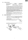
4.1.4. Battery information 4.2. Battery replacement 9 kx-tg2359bxb.
Page 10: 5 Location Of Controls
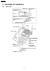
5 location of controls 5.1. Base unit 10 kx-tg2359bxb.
Page 11: 5.2. Handset
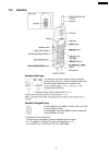
5.2. Handset 11 kx-tg2359bxb.
Page 12: 5.3. Charger Unit
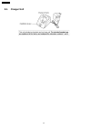
5.3. Charger unit 12 kx-tg2359bxb.
Page 13: 6 Display
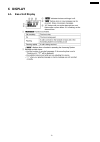
6 display 6.1. Base unit display 13 kx-tg2359bxb.
Page 14
6.2. Troubleshooting (handset lcd) the following will be displayed when the unit needs your attention. Cross reference: erasing an item in the phone book (p.37). 14 kx-tg2359bxb.
Page 15: 7 Settings
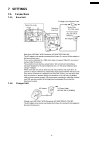
7 settings 7.1. Connections 7.1.1. Base unit 7.1.2. Charger unit 15 kx-tg2359bxb.
Page 16
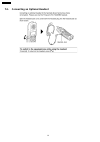
7.2. Connecting an optional headset 16 kx-tg2359bxb.
Page 17: 7.3. Function Menu Table
7.3. Function menu table cross reference: direct commands (p.22). 17 kx-tg2359bxb.
Page 18: 7.4. Date And Time
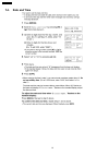
7.4. Date and time 18 kx-tg2359bxb.
Page 19: 7.5. Dialing Mode
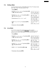
7.5. Dialing mode 7.6. Line mode 19 kx-tg2359bxb.
Page 20
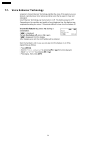
7.7. Voice enhancer technology 20 kx-tg2359bxb.
Page 21: 7.8. Ringer Tone
7.8. Ringer tone 21 kx-tg2359bxb.
Page 22: 7.9. Direct Commands
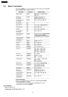
7.9. Direct commands cross reference: date and time (p.18). Copying items in the phone book (p.38). 22 kx-tg2359bxb.
Page 23: 8 Operation
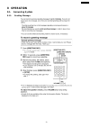
8 operation 8.1. Answering system 8.1.1. Greeting message 23 kx-tg2359bxb.
Page 24
8.1.2. Caller’s recording time 24 kx-tg2359bxb.
Page 25
8.1.3. Message alert 25 kx-tg2359bxb.
Page 26
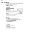
8.1.4. Erasing messages 26 kx-tg2359bxb.
Page 27: 8.3. Using The Pause Key
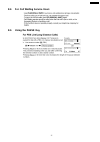
8.2. For call waiting service users 8.3. Using the pause key 27 kx-tg2359bxb.
Page 28: 8.4. Dial Lock
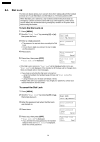
8.4. Dial lock 28 kx-tg2359bxb.
Page 29: 8.5. Flash Button
8.5. Flash button 29 kx-tg2359bxb.
Page 30
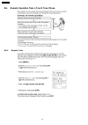
8.6. Remote operation from a touch tone phone 8.6.1. Remote code 30 kx-tg2359bxb.
Page 31
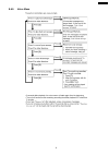
8.6.2. Voice menu 31 kx-tg2359bxb.
Page 32
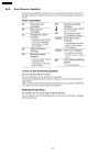
8.6.3. Direct remote operation 32 kx-tg2359bxb.
Page 33: 8.7. Phone Book
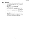
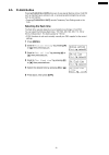
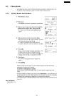
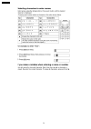
8.7. Phone book 8.7.1. Storing names and numbers cross reference: chain dial (p.36). 33 kx-tg2359bxb.
Page 34
34 kx-tg2359bxb.
Page 35
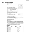
8.7.2. Dialing from the phone book 35 kx-tg2359bxb.
Page 36
8.7.3. Chain dial 36 kx-tg2359bxb.
Page 37
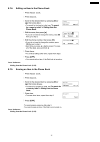
8.7.4. Editing an item in the phone book cross reference: dialing from the phone book (p.35). 8.7.5. Erasing an item in the phone book cross reference: dialing from the phone book (p.35). 37 kx-tg2359bxb.
Page 38
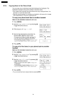
8.7.6. Copying items in the phone book 38 kx-tg2359bxb.
Page 39: 9 Troubleshooting
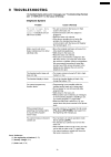
9 troubleshooting cross reference: (*1) re-registering a handset (p.53) (*2) battery charge (p.8) (*3) dial lock (p.28) 39 kx-tg2359bxb.
Page 40
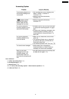
Cross reference: (*4) dial lock (p.28) (*5) message alert (p.25) (*6) connecting an optional headset (p.16) 40 kx-tg2359bxb.
Page 41
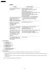
Cross reference: (*7) caller’s recording time (p.24) (*8) erasing messages (p.26) (*9) remote code (p.30) (*10) “to turn on the answering system” in direct remote operation (p.32) (*11) date and time (p.18) 41 kx-tg2359bxb.
Page 42
Cross reference: (*12) battery (p.8) (*13) connections (p.15) (*14) dialing mode (p.19) (*15) battery charge (p.8) (*16) recharge (p.8) (*17) battery replacement (p.9) (*18) date and time (p.18) note for service: in case you cannot talk on one of two handsets, replace their extension numbers as in t...
Page 43: 10.1. Base Unit
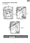
10 disassembly instructions 10.1. Base unit shown in fig.- to remove remove 1 lower cabinet screws (2.6 × 14).........(a) × 5 2 main p.C. Board tape and solder 3 screws (2.6 × 8)...........(b) × 8 43 kx-tg2359bxb.
Page 44: 10.2. Handset
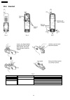
10.2. Handset shown in fig.- to remove remove 4 rear cabinet screws (2.6 × 12)........(c) × 2 5 follow the procedure. 6 main p.C. Board tape and solder 7 screw (2.6 × 12)..........(d) × 1 screws (2.6 × 9)..........(e) × 2 charge terminals 44 kx-tg2359bxb.
Page 45: 10.3. Charger Unit
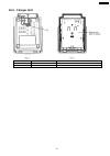
10.3. Charger unit shown in fig.- to remove remove 8 lower cabinet screw (2.6 × 12).........(f) × 1 9 main p.C. Board main p.C. Board 45 kx-tg2359bxb.
Page 46: 11 Assembly Instructions
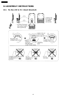
11 assembly instructions 11.1. Fix the lcd to p.C. Board (handset) 46 kx-tg2359bxb.
Page 47: 12 Troubleshooting Guide
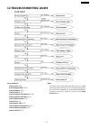
Cross reference: check power (p.48) error message table (p.48) check playback (p.50) check record (p.49) check sp-phone transmission (p.50) check sp-phone reception (p.51) check battery charge (p.51) check link (p.52) check the rf part (p.53) check handset transmission (p.57) check handset reception...
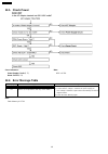
Page 48: 12.1. Check Power
Cross reference: power supply circuit (p.77) reset circuit (p.79) note: dsp is ic501. 12.1. Check power 12.2. Error message table display symptom remedy e1 the initialization was tried, but it could not be done. 1. Check the peripheral circuit of flash memory visually. 2. Confirm that the voltage is...
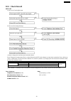
Page 49: 12.3. Check Record
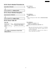
Cross reference: telephone line interface (p.80) auto disconnect circuit (p.81) parallel connection detect circuit (p.82) signal route (p.90) note: flash memory is ic701. Dsp is ic501. 12.3. Check record base unit a) not record greeting message b) not record incoming message c) how to change the aut...
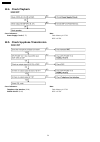
Page 50: 12.4. Check Playback
Cross reference: power supply circuit (p.77) cross reference: telephone line interface (p.80) signal route (p.90) note: flash memory is ic701. Dsp is ic501. Note: flash memory is ic701. Dsp is ic501. 12.4. Check playback 12.5. Check sp-phone transmission 50 kx-tg2359bxb.
Page 51: 12.7. Check Battery Charge
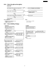
Cross reference: telephone line interface (p.80) signal route (p.90) note: flash memory is ic701. Dsp is ic501. Note: dsp is ic501. 12.6. Check sp-phone reception 12.7. Check battery charge 51 kx-tg2359bxb.
Page 52: 12.8. Check Link
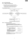
12.8. Check link (*1) refer to finding out the defective part (p.53). Cross reference: rf check flowchart (p.54) 52 kx-tg2359bxb.
Page 53: 12.9. Check The Rf Part
12.9. Check the rf part 12.9.1. Finding out the defective part after all the checkings or repairing re-register handset (to be checked) to base unit (to be checked) and hs to bu regular unit (working). 12.9.1.1. Re-registering a handset 53 kx-tg2359bxb.
Page 54
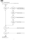
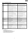
12.9.2. Rf check flowchart each item (1a ~5) of rf check flowchart corresponds to check table for rf part. Please refer to the each item. Cross reference: check table for rf part (p.55) 54 kx-tg2359bxb.
Page 55
12.9.3. Check table for rf part no. Item bu checking hs checking 1a link confirmation normal 1. Re-resister hs regular unit (working) to bu. 2. Press [talk] key of the hs regular unit to establish link. 1. Re-resister hs to bu of regular unit (working). 2. Press [talk] key of the hs to establish lin...
Page 56
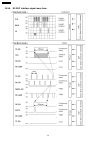
12.9.4. Rf-dsp interface signal wave form 56 kx-tg2359bxb.
Page 57: 12.12. Check Caller Id
Cross reference: signal route (p.90). Cross reference: signal route (p.90). Note: when checking the rf unit, refer to check the rf part (p.53) cross reference: telephone line interface (p.80). Calling line identification (caller id) (p.83). Note: · make sure the format of the caller id or call waiti...
Page 58: 13 Test Mode
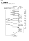
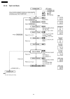
13 test mode 13.1. Test mode flow chart for base unit 13.1.1. Tx burst mode and adjust x’tal mode 58 kx-tg2359bxb.
Page 59
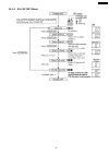
13.1.2. Rx-cw test mode 59 kx-tg2359bxb.
Page 60
13.1.3. Test link mode note: (*1) for factory use only. 60 kx-tg2359bxb.
Page 61
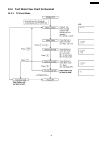
13.2. Test mode flow chart for handset 13.2.1. Tx burst mode 61 kx-tg2359bxb.
Page 62
13.2.2. Rx-cw test mode 62 kx-tg2359bxb.
Page 63
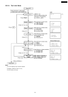
13.2.3. Test link mode note: (*1) lcd displays the channel number. (exception: default/ ch00 = 1ch.) (*2) for factory use only. 63 kx-tg2359bxb.
Page 64
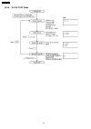
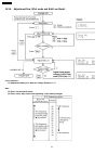
13.2.4. Adjustment flow (x’tal mode and batt low mode) cross reference (*1) adjustment battery low detector voltage (handset) (p.65) note: (*2) these are the default values. (*3) these values may not be fixed depending on the battery strength. 64 kx-tg2359bxb.
Page 65
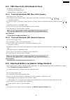
13.3. X801 (base unit), x201 (handset) check equipment: frequency counter check point for measurement: bck checking tolerance: 13.824mhz ± 100hz 13.3.1. Check and adjustment x801 (base unit) frequency 1. Set up base unit in test mode. 2. Press following keys in order to adjust crystal mode. [locator...
Page 66: Pbf
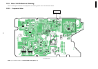
13.5. Base unit reference drawing when connecting the simulator and equipments for checking, please refer to the illustration below. 13.5.1. Component view ra705 sa102 sa101 l102 l101 p101 fl901 q351 c981 ic601 d305 c606 sa103 sa104 d101 c508 c560 c311 c308 ra703 ra704 ra501 fcs fsi fso q800 rst pdn...
Page 67
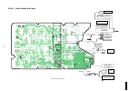
13.5.2. Flow solder side view 1 11 2 1 2 memo lcd700 rec chk dcm2 l1t l1r dcp2 dcp dcm rep txd2 ic301 ers msg ans stop q350 skip 3 pbf 45 6 7 a spp1 spm1 cp1 cm1 8 0 rdl dwn mic led720 jc1 js1 ji1 jo1 up sp uvcc1 ugnd1 utx1 urx1 hld mute fls icom r y b g micp1 micm1 9 # ant1 antg1 led721 led722 led7...
Page 68
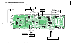
13.6. Handset reference drawing when connecting the simulator and equipments for checking, please refer to the illustration below. Ic901 ic204 ic201 ic206 ic202 ic207 cn203 pbf q207 d212 d203 d216 d215 l207 d208 d207 c302 c301 c216 c223 c267 l209 l210 d209 d220 d320 c225 c268 d217 d218 c981 l205 l20...
Page 69: 13.7. Frequency Table
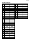
Channel tx/rx frequency (mhz) test mode frequency (mhz) 1 2400.914355 2400.724512 2 2401.808203 2401.618359 3 2402.698096 2402.508252 4 2403.591943 2403.402100 5 2404.481836 2404.291992 6 2405.375684 2405.185840 7 2406.265576 2406.075732 8 2407.159424 2406.969580 9 2408.049316 2407.859473 10 2408.94...
Page 70
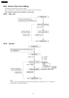
13.8. How to clear user setting the operation reset the unit to factory setting. (erase recording voice messages, stored phone numbers, caller list and etc.) this operation should not be performed for a usual repair. 13.8.1. Base unit 13.8.2. Handset note: (*1) be sure to short the battery terminals...
Page 71: 14 Description
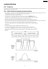
14 description 14.1. Frequency the frequency range of 2400mhz~2480mhz is used. Transmitting and receiving channel between base unit and handset is same frequency. Refer to the frequency table. 14.2. Fhss (frequency hopping spread spectrum) this telephone is using an ic chip which has similar specifi...
Page 72
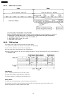
14.2.1. Tdd frame format 14.2.2. Tdma system this system is the cycles of 10ms, and has four duplex paths, so it is possible to perform four duplex communications simultaneously. In 1 slot 1.25ms, the 10ms of voice data is transmitted. Each slot makes every frame frequency hop. (100hops/sec) althoug...
Page 73
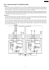
14.3. Signal flowchart in the whole system reception cn101 of the base unit is connected to the tel line, and signal is entered through the bridge diode d101. While talking, the relay (q104) is turned on and amplified at the q150, then led to dsp (ic501). The dsp encodes adpcm and tdd/tdma with fhss...
Page 74: 15.1. Calling
15 explanation of link data communication 15.1. Calling 15.2. To terminate communication 15.3. Ringing 74 kx-tg2359bxb.
Page 75
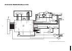
16 block diagram (base unit) rf_unit rxi tx_mod di mod_en rxgain rstn clk data le rx_en tx_en schtrl rssi key1~5 strba~f com1, com2 seg3~12 keys lcd x801 13.824khz sp_led chg_led msg_led answer_led lout lin rly dcin1 dcin0 bell cidip cidin power_down reset vccr vcc vcca vccpa hip hin spp spn chg_ctl...
Page 76
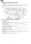
General description: 17 circuit operation (base unit) (dsp, flash memory) is a digital speech/signal processing system that implements all the functions of speech compression, record and playback, and memory management required in a digital telephone answering machine. The dsp system is fully contro...
Page 77: 17.2. Flash Memory (Ic701)
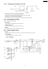
17.1.2. The meaning of the motion of pin 128 · the period of host power up (hardware initialization) in this period, the host sets up some registers in order to wake up the system. · the period of host reset (software initialization) in this period, the host reads the parameter from the memory and i...
Page 78
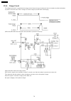
17.3.1. Charge circuit the voltage from the ac is supplied to the charge circuits. Normal charge of maximum 6-hours is started soon after the handset is placed on the base unit. Then it changes to trickle charge to prevent from overcharging. Q381 and q382 detect the on-hook state (handset is placed ...
Page 79: 17.4. Reset Circuit
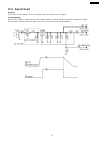
17.4. Reset circuit function: this circuit is used to initialize the microcomputer when it incorporates an ac adaptor. Circuit operation: when the ac adaptor is inserted into the unit, then the voltage is shifted by ic300 and power is supplied to the dsp. The set starts to operate when vcc goes up t...
Page 80: 17.5. Locator/intercom Mode
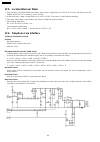
17.5. Locator/intercom mode 1. Press the base locator/intercom button, then a beep is output from pins 35 and 37 of ic501, and blinks on the sp- phone led (led 721) is caused by pin 15 of ic501. 2. At the same time, a beep is output from pin 35, pin 37 of ic501. This status is called “intercom stand...
Page 81
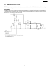
17.7. Auto disconnect circuit function: this circuit is used to detect the fact that another telephone connected to the same line is off-hook while the unit is in a receiving status or ogm transmitting status. Circuit operation: the voltage of pin50 of ic501 is monitored. If a parallel-connected tel...
Page 82
17.8. Parallel connection detect circuit function: in order to disable call waiting and stutter tone functions when using telephones connected in parallel, it is necessary to have a circuit that judges whether a telephone connected in parallel is in use or not. This circuit determines whether the te...
Page 83
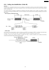
17.9. Calling line identification (caller id) function: the caller id is a chargeable id which the user of a telephone circuit obtains by entering a contract with the telephone company to utilize a caller id service. For this reason, the operation of this circuit assumes that a caller id service con...
Page 84
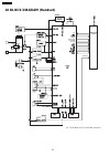
18 block diagram (handset) kx-tg2359bxb block diagram (handset) 2.5v vbatt2 3.0v ic205 d206 d213 d205 d208 d207 2 ic202 ic203 ic201 ic204 di mod_en rxgain rstn hsmip hsmin 1 int_1 int 1 84 kx-tg2359bxb.
Page 85: 19.1. Construction
19 circuit operation (handset) 19.1. Construction the circuit mainly consists of dsp and rf unit as shown in the block diagram. 19.1.1. Dsp:ic201 19.1.1.1. Function · battery low, power down defect circuit · ringer generation · interface circuit rf unit, speaker, mic, led, key scan, lcd, headset 19....
Page 86: 19.2. Power Supply Circuit
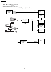
19.2. Power supply circuit voltage is supplied separately to each block. Battery +3.6v key, back light rf unit reg +2.5v ic204 dsp lcd ic201 eeprom ic202 mic circuit +3.6v vbatt2 reg +3.0v ic203 block diagram (handset power) leds +3.0v batt+ batt- charge2 charge1 d206 q212 q207 d213 d205 d208 d207 2...
Page 87: 19.3. Charge Circuit
19.3. Charge circuit when the handset is put on the cradle of the base unit or charger, the power is supplied from charge2 and charge1 terminals to charge the battery via d205 (d207), r268, q212. The voltage between charge2 and charge1 flows d213 -> r248 -> q207 -> pin80 of ic201, where the charge i...
Page 88: 19.5. Sending Signal
19.5. Sending signal the voice signal from the microphone input to dsp (42-43). Cn203 is the headset jack. When the headphone is connected, the q206 detect it. The input from the microphone of the handset (min, mip) is cut and the microphone signal from the headset is input to dsp (39). Also the pow...
Page 89
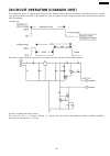
20 circuit operation (charger unit) the voltage from the ac is supplied to the charge circuits. Normal charge (165ma at the battery) of maximum 6-hours is started soon after the handset is placed on the charger unit. Then it changes to trickle charge (average 10ma at the battery) to prevent from ove...
Page 90: 21 Signal Route
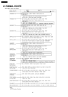
21 signal route each signal route is as follows. 90 kx-tg2359bxb.
Page 91: 22 Cpu Data (Base Unit)
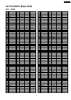
Pin description i/o high high_z low 1 int0 d.O -- -- -- 2 nc d.O -- -- -- 3 l1_bell d.I off -- on 4 l1_rly d.O off hook -- on hook 5 ac_down_det d.I high -- low 6 key_stb_f d.O active not -- 7 key_stb_e d.O active not -- 8 key_stb_d d.O active not -- 9 key_stb_c d.O active not -- 10 key_stb_b d.O ac...
Page 92: 23 Cpu Data (Handset)
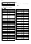
Pin description i/o high high_z low 125 vcc vcc vcc -- -- 126 nc d.O -- -- -- 127 flash_sck * high middle low 128 wdt clk d.O high -- low pin description i/o high high_z low 1 nc d.O -- -- normal 2 nc d.O -- -- normal 3 dot_lcd_rs d.O data -- instruct 4 dot_lcd_rw_ wr d.O read -- write 5 dot_lcd_e_r...
Page 93: 24.1. Ic901
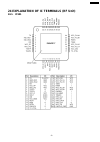
24 explanation of ic terminals (rf unit) 24.1. Ic901 93 kx-tg2359bxb.
Page 94: 25 How To Replace A
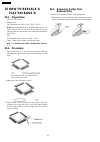
25 how to replace a flat package ic 25.1. Preparation · pbf (: pb free) solder · soldering iron tip temperature of 700°f ± 20°f (370°c ± 10°c) note: we recommend a 30 to 40 watt soldering iron. An expert may be able to use a 60 to 80 watt iron where someone with less experience could overheat and da...
Page 95
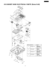
26 cabinet and electrical parts (base unit) 95 kx-tg2359bxb.
Page 96
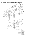
27 cabinet and electrical parts (handset) 96 kx-tg2359bxb.
Page 97
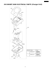
28 cabinet and electrical parts (charger unit) 97 kx-tg2359bxb.
Page 98
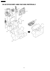
29 accessories and packing materials 98 kx-tg2359bxb.
Page 99: Diodes
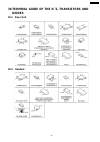
30 terminal guide of the ic´s, transistors and diodes 30.1. Base unit 30.2. Handset 99 kx-tg2359bxb.
Page 100: 30.3. Charger Unit
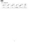
30.3. Charger unit 100 kx-tg2359bxb.
Page 101: 31 Replacement Parts
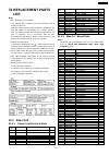
31 replacement parts list note: 1. Rtl (retention time limited) the marking (rtl) indicates that the retention time is limited for this item. After the discontinuation of this assembly in production, the item will continue to be available for a specific period of time. The retention period of availa...
Page 102
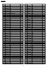
Ref. No. Part no. Part name & description remarks l901 mqlre18njf coil l903 mqlrf4n7df2 coil l904 mqlre22njf coil l905 mqlrf10njf coil l909 mqlrf3n3df2 coil l911 mqlrf2n2df2 coil l913 mqlrf10njf coil l990 pqlqr4d1r0k coil s r903 mqlre10njf coil (components parts) ra401 d1h42222a006 resistor array ra...
Page 103: 31.2. Handset
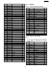
Ref. No. Part no. Part name & description remarks c511 ecue1a104kbq 0.1 c512 ecue1a104kbq 0.1 c553 ecue1a104kbq 0.1 c554 ecue1a104kbq 0.1 c560 ecst0jy106 10 c591 ecuv1c104kbv 0.1 c606 eee0ga331wp 330 c609 ecue1a104kbq 0.1 c618 ecue1h471kbq 470p c713 ecue1a104kbq 0.1 c801 ecue1a104kbq 0.1 c803 f1j0j1...
Page 104
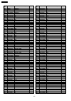
Ref. No. Part no. Part name & description remarks d217 ma8047 diode(si) s d218 ma8047 diode(si) s d219 ma8047 diode(si) s d220 ma8047 diode(si) s d903 b0dccd000011 diode(si) d904 b0dccd000011 diode(si) led201 pqvdsml310mt led s led202 pqvdsml310mt led s led203 pqvdsml310mt led s led204 pqvdsml310mt ...
Page 105: 31.3. Charger Unit
Ref. No. Part no. Part name & description remarks c311 ecue1h3r0ccq 3p c312 ecue1a104kbq 0.1 c901 ecue1h100dcq 10p s c903 ecue1h100dcq 10p s c904 ecue1h010ccq 1p s c910 ecue1h010ccq 1p s c911 ecue1h100dcq 10p s c915 ecue1h100dcq 10p s c917 ecue1h100dcq 10p s c918 ecue1h100dcq 10p s c921 ecue1h100dcq...
Page 106: 31.5. Memo
31.5. Memo 106 kx-tg2359bxb.
Page 107: 32 For Schematic Diagram
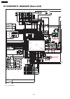
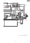
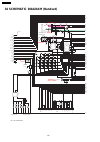
32 for schematic diagram 32.1. Base unit (schematic diagram (base unit)) notes: 1. Dc voltage measurements are taken with voltmeter from the negative voltage line. 2. This schematic diagram may be modified at any time with the development of new technology. 32.2. Handset (schematic diagram (handset)...
Page 108
33 schematic diagram (base unit) nc c745 c315 330u/6.3v c352 nc micp1 c511 k0.1 nc c743 r122 33k c420 nc c801 k0.1 micm1 c806 k0.1 spp2 spm2 mic k1.0 c502 nc c113 c553 k0.1 2.2k r416 nc c445 1k r112 r123 nc 1k r501 nc r420 c144 k0.1 txd 100 r612 nc c423 nc c741 c609 k0.1 c509 k0.1 nc c446 c382 k0.01...
Page 109
Vcc 12 r356 r151 5.6 47k r113 l102 33u d306 nc r138 r107 47k 6.8uh l376 nc c301 20v d102 r164 33(1/2w) 10m r110 1.0m r125 r157 0 q103 10u/25v c161 r166 1.2k r140 1k cp2 charge+ 15 r353 rfg q104 d377 22v cm2 chrge- 390 r352 sa102 q350 c101 680p(3216) 10k r104 c153 nc c114 k0.01 c151 k0.047 r165 680 n...
Page 110
34 schematic diagram (handset) spp cn203 1 gnd 2 mic1 3 mic2 4 sp2 5 sp1 spm 5 5 * * 6 6 1 1 3 3 4 4 up up sya # 0 0 2 2 9 9 7 7 led205 led207 led206 8 8 k0.1 c221 10k r232 q206 down down redial redial flash flash off off menu menu sp_phone sp_phone talk talk right right hold hold left left test nc ...
Page 111
R249 2.2k micp vbat k0.1 c234 vss chg2 chg1 220k r228 q205 22k r236 1k r222 nc c278 nc c276 k0.1 c203 ic202 1 a0 2 a1 3 a2 4 vss 5 sda 6 scl 7 wp 8 vcc k0.01 c231 k0.1 c224 rx tx 2.2m r234 micm rst 10k r245 pdn r247 390 13.824mhz x201 ic203 3.0v reg 1 out 3 gnd 2 in c280 k0.1 r260 100k c214 k0.1 d20...
Page 112
35 schematic diagram (rf part) nc c966 nc c958 nc c957 nc c959 ic901 1 tx 2 gnd_tx 3 gnd_rx 4 rx 5 vcc_rf 6 vcc_if2 7 testp 8 testn 9 vcc_if 10 xout 11 xin 12 vcc_bias 13 rext 14 rssi 15 rstn 16 rx_data 17 tc_ctrl 18 vcc_dig 19 vcc_pll1a 20 vcc_pll1b 21 txen 22 rxen 23 vcc_pll2b 24 vcc_pll2a 25 rxga...
Page 113
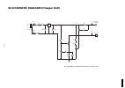
36 schematic diagram (charger unit) d2 led1 q3 q2 q4 r8 1.0k r6 1k r4 3.9 r1 2.2k r3 100 pqjt01 1 pqjt02 1 r9 56 cp cm dcp dcm c1 1u50v cn1 dc jack 2 dc+ 1 dc- ic1 1 vin 2 gnd 3 vout c2 1u50v d1 l1 4.7 µ l2 4.7 µ q5 r7 0 charge kx-tg2359bxb schematic diagram (charger unit) kx -t g235 9bx b 113.
Page 114
Memo kx -t g235 9bx b 114.
Page 115: 37.1. Component View
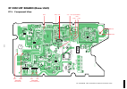
37 circuit board (base unit) 37.1. Component view c353 c911 l913 r992 r991 c904 l901 l904 r903 ra705 sa102 sa101 l102 l101 p101 fl901 d904 c910 d903 c913 c901 c939 l911 l912 c918 l903 c915 c912 c938 c903 c921 c920 ra901 r919 r354 q351 c960 c937 c961 c956 r930 c917 c922 c996 r909 c914 c981 c984 c983 ...
Page 116
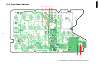
37.2. Flow solder side view 1 11 2 1 2 memo lcd700 rec chk dcm2 l1t l1r dcp2 dcp dcm rep txd2 ic301 ers msg ans stop q350 skip 3 pbf 45 6 7 a spp1 spm1 cp1 cm1 8 0 rdl dwn mic led720 jc1 js1 ji1 jo1 up sp uvcc1 ugnd1 utx1 urx1 hld mute fls icom r y b g micp1 micm1 9 # ant1 antg1 led721 led722 led724...
Page 117: 38 Circuit Board (Handset)
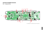
38 circuit board (handset) 38.1. Component view ic901 ic204 ic201 ic206 ic202 ic207 cn203 pbf q207 d213 d212 d203 d216 d215 l207 d208 d207 r200 c274 c278 c277 c272 c239 c234 c285 c228 c242 c240 r210 r266 r260 r225 r228 c227 c303 c302 c301 c216 c214 c215 c212 c275 c217 c230 c224 c223 c308 c307 c267 c...
Page 118
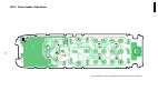
38.2. Flow solder side view 12 2 cn201 talk off up left sp_phone down menu 1 23 4 5 6 7 8 led203 led204 led201 led202 9 0 sya mic hold flash redial right led208 q213 r208 led205 ra207 c211 r217 r218 c210 ca202 ca203 led206 led207 r201 r202 r203 r204 kx-tg2359bxb circuit board (flow solder side view ...
Page 119: 39.1. Component View
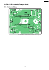
39 circuit board (charger unit) 39.1. Component view r9 r7 d2 r8 e e pqjt01 pqhg01 pqhg02 pqjt02 ic1 in pbf e r4 r3 r6 q3 e q5 q2 l2 q4 led1 d1 c1 c2 r1 l1 cn1 kx-tg2359bxb circuit board (component view (charger uint)) 119 kx-tg2359bxb.
Page 120
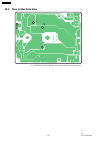
39.2. Flow solder side view cm cp dcm dcp kx-tg2359bxb circuit board (flow solder side view (charger unit)) 120 kx-tg2359bxb i.N. Kxtg2359bxb.

