- DL manuals
- Panasonic
- Camcorder
- PV-DAC10
- Service Manual
Panasonic PV-DAC10 Service Manual
Digital Video Camcorder
PV-DV100
PV-DV200
PV-DV400
PV-DV600
AC Adaptor
PV-DAC10
© 2000 Matsushita-Kotobuki Electronics Industries LTD.
All rights reserved. Unauthorized copying and distribution
is a violation of law.
ORDER NO. MKE0001400C1
ITEM
SPECIFICATION
1 2 3 4
Weight and dimensions shown are approximate.
Designs and specifications are subject to change without notice.
ITEM
SPECIFICATION
1 2 3 4
Digital Video Camera: 7.2 V DC (Battery)
7.8 V DC (AC Adaptor)
AC Adaptor: 110/120/220/240 V AC, 50/60 Hz
Battery: Lithium-Ion Type DC 7.2 V
Digital Video Camera: 7.2 V DC 6.5 W (Max. 9.5 W)
AC Adaptor: 18 W
1 W (when not in use.)
EIA Standard (525 lines, 60 fields) NTSC color signal
2 rotary heads. helical scanning system
12 bit (32 kHz) 4 tracks
16 bit (48 kHz) 2 tracks
One integral color filter Charge Coupled Device (CCD)
18:1 zoom lens, F1:1.6 with auto iris control
Focal length: 3.9 mm-70.2 mm
Power zoom function
Lens filter diameter: 49 mm
Power
Source
Power
Consumption
Video Signal
10.2 mm (0.4 inch) Electronic Viewfinder
– –
11.2 mm (0.44 inch) Liquid Crystal Electronic Viewfinder
– –
63.5 mm (2.5 inch) Liquid Crystal Display
– –
76.2 mm (3.0 inch) Liquid Crystal Display
– –
5 lx (F1:1.6) 0.5 footcandles
0 lx (IR Filter ON)
– –
0
°
C-40
°
C (32
°
F-104
°
F) (Temperature)
10 %-75 % (Humidity)
Digital Video Camera: 0.7 kg (1.54 lbs.)
– – –
0.71 kg (1.57 lbs.)
–
– –
0.68 kg (1.5 lbs.)
– –
–
0.69 kg (1.52 lbs.)
– – –
AC Adaptor:
0.18 kg (0.4 lbs.)
Digital Video Camera:
85 mm x 107.5 mm x 188 mm (W x H x D)
– –
(3-3/8 inch x 4-1/4 inch x 7-3/8 inch)
85 mm x 107.5 mm x 163 mm (W x H x D)
– –
(3-3/8 inch x 4-1/4 inch x 6-3/8 inch)
AC Adaptor: 103 mm x 40 mm x 79 mm (W x H x D)
(4 inch x 1-5/8 inch x 3-1/8 inch)
Video
Recording
System
Audio
Pick-Up
System and
Device
Lens
Viewfinder
LCD Monitor
Minimum
Illumination
Required
Operating
Condition
Weight
Dimensions
Models: PV-DV100/ PV-DV200
PV-DV400/ PV-DV600
Model: PV-DAC10
R
TM
R
1. PV-DV100
2. PV-DV200
3. PV-DV400
4. PV-DV600
Mini
Summary of PV-DAC10
Page 1
Digital video camcorder pv-dv100 pv-dv200 pv-dv400 pv-dv600 ac adaptor pv-dac10 © 2000 matsushita-kotobuki electronics industries ltd. All rights reserved. Unauthorized copying and distribution is a violation of law. Order no. Mke0001400c1 item specification 1 2 3 4 weight and dimensions shown are a...
Page 2: Table of Contents
Block diagrams ccd drive block diagram ............................................ 6-1 video signal process i block diagram ......................... 6-2 video signal process ii block diagram ........................ 6-4 analog video i/f block diagram ................................... 6-5 audio s...
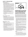
Page 3: Prevention of Electro
1-1 general guidelines 1. Important safety notice there are special components used in this equipment which are important for safety. These parts are marked by in the schematic diagrams, circuit board layout, exploded views and replacement parts list. It is essential that these critical parts should...
Page 4: X-Radiation (Model: A,
1-2 x-radiation (model: a, b) warning : 1. The potential source of x-radiation in evf sets is the high voltage section and the picture tube. 2. When using a picture tube test jig for service, ensure that jig is capable of handling 10 kv without causing x-radiation. Note : it is important to use an a...
Page 5: Service Notes
1-3 service notes note : 1. The lcd open/close sw. Is for changing between lcd display or evf display. When turning on lcd display, place some paper or tape, etc. On lcd open/close sw. So that this sw. Stays on. 2. Use a grounded esd wrist strap while disassembling the lens portion. 3. Use extreme c...
Page 6
1-4 fig. 1-2 analog c.B.A. (model: d) note 1 note: marked parts are supplied as service fixtures. Mechanism chassis ass’y head amp c.B.A. Head amp f.P.C. Cylinder f.P.C. Mechanism sensor f.P.C. Capstan f.P.C. Lcd f.P.C. Lens f.P.C. Ccd f.P.C. Mechanism f.P.C. Lcd c.B.A. Lens unit lcd open/close sw. ...
Page 7
1-5 interconnection of extension cables fig. 2 lens unit ccd f.P.C. Lens f.P.C. Capstan f.P.C. Cylinder f.P.C. Mechanism sensor f.P.C. Head amp f.P.C. Head amp c.B.A. Mechanism f.P.C. Lcd f.P.C. Lcd c.B.A. Jack c.B.A. Front c.B.A. Mechanism chassis ass'y main c.B.A. Power c.B.A. Analog c.B.A. (model...
Page 8
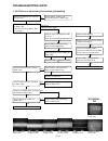
1-6 simplified fault finding data (self-diagnostic system) when following conditions occur, the power led will flash according to the condition. Fig. 3 power led condition t-reel lock s-reel lock unloading lock loading lock cylinder lock after 1 minute flash, power will be turned off. After 1 minute...
Page 9
1-7 method for loading/unloading of mechanism caution: if loading does not start after dc power supply is applied, do not continue to applying dc power supply. Apply +3 vdc power supply to the loading motor terminals. Loading: dc - to portion "a," dc + to portion "b" unloading: dc + to portion "a," ...
Page 10
1-8 how to remove a jammed tape electrical method caution: if loading does not start after dc power supply is applied, do not continue to applying dc power supply. In this case, perform in manual method. Remove a jammed tape as follows: (1) remove the cabinet parts. Refer to "cabinet section" in dis...
Page 11
1-9 eeprom data caution: be sure to save the eeprom data using pc-evr adjustment program before service and adjustment in order to make sure to avoid an accidental data loss, etc. As follows. There are two eeprom in this unit. 1 how to save the eeprom data to your pc 1. How to save the eeprom data f...
Page 12
1-10 how to use the dvc head cleaning tape / lsuq0003 please use the cleaning tape as described below. How to replace the lamp (vllw0023) of enhancement light unit (model: d) danger: to prevent possible burn hazard, disconnect this unit and allow lamp to cool before replacing. Replace only with vllw...
Page 13
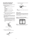
1-11 replacement procedure for leadless (chip) component the following procedures are recommended for the replacement of the leadless components used in this unit. 1. Preparation for replacement a. Soldering iron use a pencil-type soldering iron using less than 30 watts. B. Solder eutectic solder (t...
Page 14
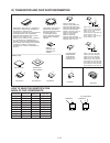
1-12 y 2sd1819 b 2sb1218a 1r 2sb970 u 2sc3931 1x 2sc3938 s 2sc3929 1r 2sb1585 t 2sd1119 mc ma143 1b ma111 ic, transistor and chip part information general c.B.A./ass'y parts b 2sc4081t106r b 2sb709a 6d un5114 f 2sa1037l146r 8c un5213 8b un5212 6e un5115 z 2sd601a g 2sk1958 z 2sd1819a marking part no...
Page 15
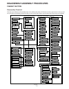
2-1 disassembly flowchart this flow chart indicates the disassembly steps of the cabinet parts and the p.C.Boards in order to gain access to item (s) to be serviced. When reassembling, perform the step (s) in the reverse order. Bend, route and dress the wires as they were originally. Cabinet section...
Page 16
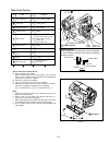
2-2 fig. D3 fig. D2 (s-1) view a fp4801 of front c.B.A. Front c.B.A. Main c.B.A. Front cable fp10 of main c.B.A. Open reassembly note: when installing the front case unit, connect it between fp10 and fp4801 so that the front cable is positioned correctly as shown. (s-1) front case unit 1 (s-2) view ...
Page 17
2-3 fig. D6 (s-8) slot of ir filter plate (model: c, d) slot of ir filter plate (model: c, d) (l-1) rubber of ir filter knob (model: c, d) rubber of ir filter knob (model: c, d) reassembly note: when installing the lens unit, install so that the rubber of ir filter knob inserts to slot of ir filter ...
Page 18
2-4 fig. D10 front case unit portion fig. D9 hood screw 3 lens ring hood piece shoe 2 ir panel (model: c, d) 4 front case unit (s-3) (s-2) (l-1) front c.B.A. 1 front case unit (s-1) step /loc. No. Part remove fig. No. Front c.B.A. D9 2(s-1) 1 shoe d10 (s-2) 2 3 4 hood screw d10 3(s-3), lens ring, ho...
Page 19
2-5 side case r unit portion fig. D12 fig. D11 (s-1) (l-1) side case r unit note: (1)to gain access 2 screws (s-1), close the lcd case unit, or turn it to the right or left. (2)work carefully so as not to damage f.P.C. Bosses slot slot lcd case unit 1 unsolder (s-4) speaker unit 3 right cover unit 2...
Page 20
2-6 fig. D14 lcd portion fig. D15 lcd case a unit 1 (s-1) turn (l-1) (l-1) (l-1) lcd case b unit (lcd case unit) lcd shaft unit note: to gain access to 2 screws (s-1), turn the lcd shaft unit to the right or left. Lcd unit 3 2 4 (s-2) (s-3) note: when removing the lcd case b, pull the lcd unit out o...
Page 21
2-7 fig. D16 fig. D17 lcd c.B.A. 5 lcd panel unit 6 (l-2) (l-2) lcd lamp unit (l-2) (l-2) lead light panel unit fp8003 unsolder unsolder when replacing the lead light panel unit , make sure to remove protection sheet as shown below. Use extreme care when handling the lead light panel unit and the lc...
Page 22
2-8 lens portion a fig. D18 fig. D19 caution: (1) when removing the ccd c.B.A., take care so that the optical filter does not fall out. (2) take extreme care when removing the ccd because it is easily damaged by static electricity. Use a wrist strap while removing and installing. (3) do not apply he...
Page 23
2-9 fig. D20 fig. D21 lens portion b 3 ir filter plate (model: c, d) (s-1) (s-1) (s-2) lens unit slot pin of ir lever (model: c,d) 1 lens piece unit note: when installing the ir filter plate, install so that the pin of ir lever is inserted to slot of ir filter plate. After installing, confirm that t...
Page 24
2-10 fig. D22 side case l unit portion view a push jack cover jack cover open 3 strap angle strap angle 2 jack ass'y 1 in/out knob (model: d) 4 (s-1) in/out switch (model: d) (s-2) hand strap (l-1) view a note: when removing the strap angle, push strap angle lower portion to release as shown. Do not...
Page 25
2-11 fig. D23 fig. D24 jack c.B.A. 7 jack angle 8 s-jack c.B.A. 6 jack f.P.C. 5 (s-4) fp3701 hole (s-3) fp3751 zoom switch unit 10 battery eject piece 9 (s-5) portion b slot of mmc exchange knob (model: b, c, d) slot of mmc exchange knob (model: b, c, d) tab of switch (model: b,c,d) tab of switch (m...
Page 26
2-12 top case unit portion fig. D25 fig. D26 color evf unit (model: c, d) or evf unit (model: a, b) 2 top case unit 1 (s-1) (s-2) (l-1) top angle 3 top connector cable 4 top operation unit 5 connector (s-3) (l-2) boss (l-3) step /loc. No. Part remove fig. No. Top case unit d25 d25 d26 d26 (s-1), (s-...
Page 27
2-13 evf unit portion (model: a, b) note: when disassembling or reassembling, make sure that no dust gets in evf unit. Fig. D27 eye cap unit 1 evf case unit (l-1) turn (l-1) view a note: the eye cap unit is very tight. Use extreme so as not to damage the unit. Eye sight ring evf f.P.C. Holder evf f....
Page 28
2-14 fig. D28 fig. D29 (s-2) (s-1) (l-2) (l-2) evf angle unit 2 evf f.P.C. Holder 3 fig. D30 evf case a unit 4 dust cover 5 (s-3) (l-3) evf esd angle unit 6 evf case b 7 crt 9 deflection yoke 10 evf c.B.A. 11 p902 fp801 evf f.P.C. 8 crt socket unit deflection yoke deflection yoke 5.35 mm 1.35 mm ano...
Page 29
2-15 fig. D32 fig. D31 color evf unit portion (model: c, d) note: when disassembling or reassembling, make sure that no dust gets in color evf unit. Eye cap unit 1 push (s-1) evf f.P.C. Holder reassembly notes: when installing the eye cap unit, tighten 2 screws (s-1) while pushing as indicated by th...
Page 30
2-16 fig. D34 fig. D33 evf fixing angle 5 lcd evf case 6 evf f.P.C. 7 (s-3) (l-2) (l-2) (s-3) lcd evf angle unit 8 evf f.P.C. Holder note: work carefully so as not to damage the f.P.C. 4 (l-1) (l-1) evf protect a 10 color evf a c.B.A. 9 color evf b c.B.A. 12 led diffusion plate 13 led lens 14 evf lc...
Page 31
2-17 mechanism section disassembly method this procedure starts with the condition that the cabinet parts and main c.B.A. Have been removed. When reassembling, perform the step(s) in the reverse order. Perform all disassembly/reassembly and alignments procedures in stop position except disassembly/r...
Page 32
2-18 top view inner parts location note: box indicates alignment (gear alignment or tape path alignment with l.I.S.T.A.) required when a part is replaced. 24 26 1 5 6 38 19 32 40 20 21 4 2 9 13 27 14 28 30 16 15 31 41 42 17 3 head amp c.B.A. Garage unit guide piece l guide piece r cylinder unit dump...
Page 33
2-19 fig. Dm1-2 bottom view 7 8 33 34 36 37 39 dew sensor mechanism f.P.C. Unit mode switch 35 mic switch main plate unit t4 drive arm drive pulley timing belt 23 t arm unit 22 s arm unit.
Page 34
2-20 stop position confirmation check the following points to confirm that the mechanism is in stop position from the top side. Fig. Dm2 top view s post unit end of the guide slots end of the guide slots pinch arm unit t4 height plate s connection gear unit s reel table through hole t post unit shou...
Page 35
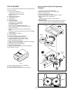
2-21 head amp c.B.A. Fig. Dm3 cylinder unit fp5001 (on head amp c.B.A.) (s-1) 1 head amp c.B.A. (s-1) (l-1) disassembly notes: 1. Use extreme care when disconnecting the connector f5001 on head amp c.B.A. Do not touch the video heads during servicing. Perform all disassembly/reassembly and alignment...
Page 36
2-22 guide piece l, guide piece r, garage unit fig. Dm4 4 garage unit pin a shaft of garage unit hole a gear of dumper unit 2 guide piece l 3 guide piece r pin a hole a pin b push slide slot b pin b slot b lock lever (s-2) (l-2) (l-2) (s-2) reassembly notes: 1. Installation of garage unit 1) install...
Page 37
2-23 cylinder unit fig. Dm5 5 cylinder unit (s-3) bosses reassembly notes: 1. Installation of cylinder unit 1) install the cylinder unit so that 2 holes on the cylinder unit surface fit over the 2 bosses on the chassis. Then, tighten 3 screws (s-3). Disassembly notes: 1. Use extreme care when removi...
Page 38
2-24 dumper unit fig. Dm6 6 dumper unit (s-4).
Page 39
2-25 dew sensor fig. Dm7 7 dew sensor sheet portion a unsolder screwdriver dew sensor chassis unsolder caution: do not touch the element part 0 mm ~ 2 mm view a view a 4 mm ~ 7 mm 3 mm ~ 5 mm dew sensor leads reassembly notes: 1. Installation of dew sensor 1) put the dew sensor on chassis with adhes...
Page 40
2-26 mechanism f.P.C. Unit fig. Dm8 8 mechanism f.P.C. Unit solder (safety switch x2) sensor holder r lock lever unit cassette down switch double-sided adhesive tape sensor holder l sensor sensor sensor sensor holder l sensor lock lever lock lever slide slide view a sensor holder r cassette down swi...
Page 41
2-27 reduction gear b fig. Dm9 9 reduction gear b gear of mode switch note: this hole on reduction gear is not used to align. Gear of loading motor unit (c-1).
Page 42
2-28 mechanism cover unit fig. Dm10 reassembly notes: 1. Installation of mechanism cover unit 1) before installing, place the mechanism in stop position by rotating the mode switch. 2) turn the gear on reverse side of mechanism cover unit counterclockwise as shown. 3) install the mechanism cover uni...
Page 43
2-29 idler arm unit, center gear fig. Dm11 reassembly notes: 1. Installation of idler arm unit and center gear 1) set the center gear into idler arm unit so that hole on idler arm unit are through holes. Confirm that the small gear of center gear engages with gear of idler arm unit. 2) install both ...
Page 44
2-30 tension arm unit fig. Dm12 reassembly notes: 1. Installation of tension arm unit 1) before installing the tension arm unit, place the mechanism in stop position by rotating the mode switch, (confirm that the s connection gear unit is separated from s reel gear.) and then hook the spring of tens...
Page 45
2-31 s reel table, t reel table fig. Dm13 14 s reel table 15 t reel table pin pin (w-1) (w-1) (c-4) (c-4) gear of t brake unit reassembly notes: 1. Installation of s reel table and t reel table 1) install 2 washers (w-1) onto each pins. 2) confirm that the gear of t reel table engages with the gear ...
Page 46
2-32 s connection gear unit fig. Dm14 16 s connection gear unit hooking portion slide spring projection on sensor f.P.C. Projection on sensor f.P.C. Reassembly notes: 1. After installing the s connection gear unit, confirm that the s connection gear unit can slide smoothly. Disassembly notes: 1. Whe...
Page 47
2-33 t break unit fig. Dm15 17 t brake unit (l-5) (s-7) plate disassembly notes: 1. When removing the t brake unit, remove screw (s-7) and the plate. Then, remove the t brake unit while releasing the locking tab (l-5). 2. Use extreme care when removing the t brake unit. If locking tab (l-5) is broke...
Page 48
2-34 t4 height plate, pinch arm unit fig. Dm16 18 t4 height plate spring slide see reassemly notes. Hooking portion a spring (s-8) 19 pinch arm unit hole (through hole) hooking portion a hooking portion b t4 drive arm pin pin a hole a slot hooking portion b reassembly notes: 1. Installation of pinch...
Page 49
2-35 rail fig. Dm17 20 rail (l-7) s post t post (s-9) slide slide (l-6) reassembly notes: 1. Installation of rail 1) set 4 locking tabs (l-7), and then push down the rail to set locking tab (l-6) firmly. Disassembly notes: 1. Before removing the rail, slide the s & t posts by rotating the mode switc...
Page 50
2-36 cylinder base unit fig. Dm18 reassembly notes: 1. Before installing the cylinder base unit, confirm that the s & t posts are lowered. 2. When installing, tighten 3 screws (s-11a), (s-11b) and (s- 11c) in order first. Then, tighten screw (s-10). 3. After installing, slide the s & t posts to inse...
Page 51
2-37 s & t arm unit, s & t post unit fig. Dm19 reassembly note: 1. Alignment/installation of s & t post unit, s & t arm unit 1) install the s arm unit to the s post unit while passing the projection. 2) install the t arm unit to the t post unit while passing the projection. 3) confirm that the hole ...
Page 52
2-38 loading motor unit fig. Dm20 26 loading motor unit (s-11) chassis holes bosses.
Page 53
2-39 sensor f.P.C. Fig. Dm21 27 sensor f.P.C. (s-13) pins holes holes slide slide pins (s-13) reassembly notes: 1. Installation of sensor f.P.C. 1) install the sensor f.P.C. So that pins on chassis are in holes on the sensor f.P.C. 2) slide the sensor f.P.C., and then tighten 2 screws (s- 13). Disas...
Page 54
2-40 tension drive arm, s brake drive lever fig. Dm22 29 s brake drive lever 28 tension drive arm cam follower pin cam follower pin outside groove inside groove cam gear intermediate gear main plate unit mode switch reassembly notes: 1. Installation of s brake drive lever, tension drive arm 1) confi...
Page 55
2-41 cam gear fig. Dm23 30 cam gear hole (through hole) main plate unit mode switch hole (through hole) half circle mark circle indent a circle indent b circle indent intermediate gear line up line up reassembly notes: 1. Alignment of intermediate gear, main plate unit, mode switch, cam gear 1) befo...
Page 56
2-42 pinch drive arm, intermediate gear fig. Dm24 32 intermediate gear 31 pinch drive arm pin on main plate unit pin on main plate unit slot.
Page 57
2-43 mode switch fig. Dm25 33 mode switch (s-14) chassis hole boss reassembly notes: 1. When installing the mode switch, install the mode switch without tottering.
Page 58
2-44 mic switch fig. Dm26 34 mic switch (s-15) bosses chassis holes.
Page 59
2-45 main plate unit fig. Dm27 35 main plate unit pin on t4 drive arm slots guide pin on chassis guide pin on chassis pin reassembly notes: 1. Installation of main plate unit 1) install the main plate unit so that pin on t4 drive arm and guide pin on chassis are in slots on main plate unit correctly...
Page 60
2-46 t4 drive arm fig. Dm28 36 t4 drive arm.
Page 61
2-47 drive pulley fig. Dm29 37 drive pulley timing belt groove of drive pulley timing belt "a" "b" "c" "d" "d" reassembly notes: 1. Do not let the timing belt twist. Be careful so as not to let the timing belt touch the greased portion. 2. When installing the drive pulley, confirm that the timing be...
Page 62
2-48 capstan unit, timing belt, capstan adjust spring fig. Dm30 39 timing belt 38 capstan unit 40 capstan adjust spring pin a pin a pin b hole (s-17) (s-16) groove of capstan unit pin b boss reassembly notes: 1. When installing the capstan unit, hook the timing belt to the groove of capstan unit..
Page 63
2-49 lock lever unit, lock pick lever fig. Dm31 42 lock pick lever guide pin on chassis lock lever spring slot 41 lock lever unit (c-5) hooking portion pin a pin b slot slot slot hole reassembly notes: 1. Installation of lock lever unit 1) install the lock lever unit so that pin a and pin b are inse...
Page 64: Adjustment Procedures
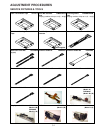
3-1 service fixtures & tools adjustment procedures dvc head cleaning tape lsuq0003 reel fg adjustment cassette 49% transmission tape vfk1217 color bar standard tape (keeping condition: keep at 18 c ~ 28 c) vfm3010ehs linear alignment tape vfm3000ehsm extension cable 40p extension cable 20p (2 pcs) l...
Page 65
3-2 light box and ac adaptor vfks002y infinity lens (with focus chart) grease lsuq0002 vfks0081 grease vfk1164tcm02 lsup0010 lsup0007 49mm ring vfk1164tar49 color conversion filter (c14) mic reader (ac 100v) vfk1164tfct2 color conversion filter (c10) satellite box (ac 100v) atf i/f (ac 100v) rs-232c...
Page 66
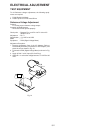
3-3 electrical adjustment introduction most of electrical adjustments can be adjusted using personal computer with pc-evr adjustment software. The set-up of pc-evr adjustment and the vr (variable resister) adjustment procedure are described in this section. For adjustment item (section) for the mode...
Page 67
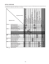
3-4 initial guideline the table below shows which adjustments are necessary according to the unit parts and individual parts to be replaced. Make sure to perform these adjustments shown below as necessary. Main c.B.A. Ic301(eeprom) ic303(camera digit al signal process) ic703(hall amp) ic3001(viola) ...
Page 68
3-5 test equipment to do all of these electrical adjustments, the following equip- ments are required. 1. Dual-trace oscilloscope voltage range: 0.001 to 50 v/div. Frequency range: dc to 50 mhz probes: 10:1, 1:1 2. Dvm (digital volt meter) 3. Frequency counter 4. Vectorscope 5. Plastic tip driver 6....
Page 69
3-6 preparation 1. Open the lcd panel. Lcd panel fig. E3-1 2. Remove screws (a), the right cover unit and the short jig c.B.A. From the unit. Screws (a) short jig c.B.A. Right cover unit fig. E3-2 3. Connect the camera connecting cable to p101 and p102 on the interface board. Camera connectiong cabl...
Page 70
3-7 personal computer connect to rs232c connector dvc p101 p102 camera connecting cable operation panel inter link cable interface board p108 sw109 (iris) sw111 (5 v sel) sw113 (power on) sw115 (m103 exmod1) sw110 (rs232c sel) sw114 (m103 vpp) sw103 (reci) sw108 (bst test) fig. E3-5.
Page 71
3-8 set up of pc-evr adjustment program 1. Turn on the personal computer. Windows ® 95 will be set up automatically. 2. Restart it in ms-dos mode. 3. Change the current directory to the one including the pc- evr adjustment program and start up the pc-evr adjust- ment program as follows. 1) if ms-dos...
Page 72
3-9 vr adjustment monochrome evf section note: camcorder need not to be powered off and on after each adjustment procedure. Preparation 1. Before adjusting the monochrome evf, camera section and vcr section adjustments must be completely ad- justed. 2. Remove the evf angle unit, the evf case a unit,...
Page 73
3-10 brightness adjustment purpose: to set the optimum evf brightness level. Symptom of misadjustment: the evf picture will be too white or black. Test point : ---------- adjustment : vr903 (evf c.B.A.) specification: natural gradation input : color bar chart mode : camera equipment : viewfinder adj...
Page 74
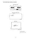
3-11 test points and control location test point information test point with no test pin. Color evf a c.B.A. (c, d) evf c.B.A. (a, b) (foil side) (foil side) lcd c.B.A. (component side) tp8003 tp8002 tp8006 tp8007 tp8001 vr901 vr902 vr903 vertical size brightness focus tp901 tp903 tp905 tp902.
Page 75
3-12 tape path alignment with l.I.S.T.A. 1. Over view a. What is lista: the lista is a new linearity alignment system with personal computer. It is newly developed to achieve precise alignment for dv format. The lista system mainly consists of personal computer, satellite box, mic reader and atf i/f...
Page 76
3-13 set sw104(bst_test) to [normal]. Set sw106(rec_i) to [off]. G. Interface board sw104(bst-test) sw106(rec-i) cag cable(36pin) mic cable(36pin) mcs cable(14pin) atf cable(14pin) h. Linear alignment tape(vfm3000ehsm) (keeping condition: keep at 18 ° c ~ 28 ° c) i. Post height adjustment fixture(vf...
Page 77
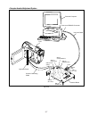
3-14 3. Connections a) interconnection of lista system. Personal computer interface board camera connecting cable rs-232c cable gp-ib cable mic reader atf i/f satellite box camcorder cag cable mcs cable mic cable atf cable caution: ac power source of following equipments are 100v ac. Use 100v ac pow...
Page 78
3-15 c) connect the mic cable of interface board and the mic reader. Interface board mic cable mic reader d) connect the mic reader and personal computer with the rs-232c cable. 1) connect the rs-232c cable to the mic reader. Rs-232c cable mic reader 2) connect the rs-232c cable to the personal comp...
Page 79
3-16 e) connect the mcs cable of interface board and satellite box. Mcs cable satellite box interface board f) connect the satellite box and personal computer with the gp-ib cable. Personal computer gp-ib cable satellite box.
Page 80
3-17 g) connect the cag cable of interface board and personal computer. 1) connect the cag cable to the personal computer. Personal computer cag cable interface board h) connect the atf cable of interface board and atf i/f. Pk5 pi atf cable interface board atf i/f "set to pk5".
Page 81
3-18 4. Getting start 1. Confirm sw setting of the interface board as follows. Set sw104(bst_test) to [normal]. Set sw106(rec_i) to [off]. 2. Turn on the personal computer. 3. Main menu appears. 4. Start up the pc-evr adjustment program refer to “set up of pc-evr adjustment program” and select “ente...
Page 82
3-19 5. Explanation for “ave.10” display (a) function key 1 : to display the ten times average data of linear curve. (b)* function key 2 : to display the three times average data of linear curve. (c)* function key 3 : to set base sampling number for average data. (d)* function key 4 : to display the...
Page 83
3-20 6. Envelope adjustment note: this adjustment is required when the indicator color becomes red in “step 10” of “4. Getting start.” if it becomes blue, this adjustment need not to be performed. Purpose: to make sure that the tape path is well stabilized. Symptom of misadjustment: if the tape trav...
Page 84
3-21 make this part flat (square) as possible. Oscilloscope s1 post t1 post oscilloscope before adj. After adj. 6) after adjustment of step 4) and 5), confirm the indicator color in the confirmation area once again to confirm if further adjustment is necessary or not. If it is blue, the adjustment i...
Page 85: Schematic Diagrams
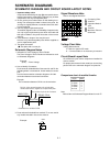
4-1 schematic diagrams schematic diagram and circuit board layout notes 1. Important safety notice components identified by the sign have special charac- teristics important for safety. When replacing any of these components. Use only the specified parts. 2. Do not use the part number shown on this ...
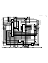
Page 86
4-2 note: for schematic diagram and circuit board layout notes, refer to beginning of schematic section. Comparison chart of models & marks pv-dv100 pv-dv200 pv-dv400 pv-dv600 not used a b c d z model mark main i (overall) schematic diagram r3901 0 r3902 0 r3903 0 r3904 0 r9001 0 r9003 r9004 r9002 0...
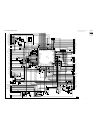
Page 87
4-3 note: for schematic diagram and circuit board layout notes, refer to beginning of schematic section. Comparison chart of models & marks pv-dv100 pv-dv200 pv-dv400 pv-dv600 not used a b c d z model mark main ii (control) schematic diagram q6001 un5115 c6009 10/6.3v q6007 2sb970 d6003 ma111 d6004 ...
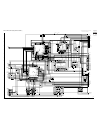
Page 88
4-4 note: for schematic diagram and circuit board layout notes, refer to beginning of schematic section. Comparison chart of models & marks pv-dv100 pv-dv200 pv-dv400 pv-dv600 not used a b c d z model mark main iii (camera signal process) schematic diagram (a) c703 47/16v q701 2sd1819a c706 47/16v q...
Page 89
4-5 note: for schematic diagram and circuit board layout notes, refer to beginning of schematic section. Comparison chart of models & marks pv-dv100 pv-dv200 pv-dv400 pv-dv600 not used a b c d z model mark main iii (camera signal process) schematic diagram (b, c, d) c703 47/16v ic701 lb1837m-te-l 1 ...
Page 90
4-6 note: for schematic diagram and circuit board layout notes, refer to beginning of schematic section. Comparison chart of models & marks pv-dv100 pv-dv200 pv-dv400 pv-dv600 not used a b c d z model mark main iv (video i) schematic diagram l3005 10 l3006 10 10 l3009 10 l3010 10 l3003 un5212 q3005 ...
Page 91
4-7 note: for schematic diagram and circuit board layout notes, refer to beginning of schematic section. Comparison chart of models & marks pv-dv100 pv-dv200 pv-dv400 pv-dv600 not used a b c d z model mark wf3 c3231 c3232 l3203 10 l3201 10 c3221 c3219 22/4v c3207 c3214 0.01 c3203 0.1 0.01 c3233 c320...
Page 92
4-8 note: for schematic diagram and circuit board layout notes, refer to beginning of schematic section. Comparison chart of models & marks pv-dv100 pv-dv200 pv-dv400 pv-dv600 not used a b c d z model mark main vi (audio) schematic diagram 10 l4002 l4001 10 10k r4013 27k r4007 2200 r4016 10k r4006 0...
Page 93
4-9 note: for schematic diagram and circuit board layout notes, refer to beginning of schematic section. Comparison chart of models & marks pv-dv100 pv-dv200 pv-dv400 pv-dv600 not used a b c d z model mark main vii (drive) schematic diagram c2023 0.1 c2014 0.1 c2003 1000p c2022 47p c2025 0.1 c2002 0...
Page 94
4-10 note: for schematic diagram and circuit board layout notes, refer to beginning of schematic section. Comparison chart of models & marks pv-dv100 pv-dv200 pv-dv400 pv-dv600 not used a b c d z model mark lower saturation detect lower saturation detect hall amp matrix upper saturation detect cap m...
Page 95
4-11 note: for schematic diagram and circuit board layout notes, refer to beginning of schematic section. Comparison chart of models & marks pv-dv100 pv-dv200 pv-dv400 pv-dv600 not used a b c d z model mark main viii (sub power) schematic diagram r1113 47k q1105 2sb1462j c1101 2.2 q1106 2sb1462j q11...
Page 96
4-12 note: for schematic diagram and circuit board layout notes, refer to beginning of schematic section. Comparison chart of models & marks pv-dv100 pv-dv200 pv-dv400 pv-dv600 not used a b c d z model mark s-jack schematic diagram jk3702 1 2 3 4 5 bk1608hm102 l3701 bk1608hm102 l3702 bk1608hm102 l37...
Page 97
4-13 note: for schematic diagram and circuit board layout notes, refer to beginning of schematic section. Comparison chart of models & marks pv-dv100 pv-dv200 pv-dv400 pv-dv600 not used a b c d z model mark head amp schematic diagram 680p c5009 r5003 r5004 0.01 c5004 10 l5002 l5003 0.01 c5007 270 r5...
Page 98
4-14 note: for schematic diagram and circuit board layout notes, refer to beginning of schematic section. Comparison chart of models & marks pv-dv100 pv-dv200 pv-dv400 pv-dv600 not used a b c d z model mark analog schematic diagram (d) ic3504 1 gnd 2 v_in 3 h_bias 4 hd_out 5 no_sync 6 osc 7 nc 8 sl_...
Page 99
4-15 note: for schematic diagram and circuit board layout notes, refer to beginning of schematic section. Comparison chart of models & marks pv-dv100 pv-dv200 pv-dv400 pv-dv600 not used a b c d z model mark power schematic diagram l1002 33 l1005 33 c1033 3.3 r1016 1k r1007 27k c1002 0.47 c1003 0.1 c...
Page 100
4-16 note: for schematic diagram and circuit board layout notes, refer to beginning of schematic section. Comparison chart of models & marks pv-dv100 pv-dv200 pv-dv400 pv-dv600 not used a b c d z model mark microphone unit/front schematic diagram c4814 4700p q4810 2sd1819a r4809 10k d6501 sml010lt-m...
Page 101
4-17 note: for schematic diagram and circuit board layout notes, refer to beginning of schematic section. Comparison chart of models & marks pv-dv100 pv-dv200 pv-dv400 pv-dv600 not used a b c d z model mark ccd schematic diagram r605 330 r606 390 r607 1200 q601 xp4601 c616 68p l601 6.8 ic602 mn37290...
Page 102
4-18 note: for schematic diagram and circuit board layout notes, refer to beginning of schematic section. Comparison chart of models & marks pv-dv100 pv-dv200 pv-dv400 pv-dv600 not used a b c d z model mark evf schematic diagram (a, b) 150p c910 1/50v c917 ma111 d901 33k r917 24k r920 220b vr901 1m ...
Page 103
4-19 note: for schematic diagram and circuit board layout notes, refer to beginning of schematic section. Comparison chart of models & marks pv-dv100 pv-dv200 pv-dv400 pv-dv600 not used a b c d z model mark color evf a/b schematic diagram (c, d) r931 2200 r901 22/6.3v c912 2sd1819a q901 0.1 c911 r93...
Page 104
4-20 note: for schematic diagram and circuit board layout notes, refer to beginning of schematic section. Comparison chart of models & marks pv-dv100 pv-dv200 pv-dv400 pv-dv600 not used a b c d z model mark lcd schematic diagram c8001 ep10qy03te8l d8102 15p c8110 un5212 q8005 15 l8005 0.1 c8020 4.7/...
Page 105
4-21 note: for schematic diagram and circuit board layout notes, refer to beginning of schematic section. Comparison chart of models & marks pv-dv100 pv-dv200 pv-dv400 pv-dv600 not used a b c d z model mark interconnection schematic diagram 1 2 3 4 5 6 7 8 9 10 11 12 13 14 15 16 17 18 19 20 21 22 23...
Page 106
4-22 wf1 wf2 wf3 wf4 wf5 wf6 wf7 wf8 wf9 wf10 wf11 wf12 wf13 wf14 wf15 wf16 wf17 wf18 wf19 wf20 wf21 wf22 wf23 wf24 wf25 lcd c.B.A. Color evf c.B.A. (c, d) analog c.B.A. (d) main c.B.A. / ccd c.B.A. Wf26 wf27 wf28 wf29 pin 13 of fp5 20 mv 1 ms1 pin 6 of ic3204 0.2 v 20 µs1 tp3207 1.0 v 50 ns1 tp3206...
Page 107
4-23 mode camera pin no. Mode camera pin no. Mode camera pin no. Mode camera pin no. Mode camera pin no. Mode camera pin no. Mode camera pin no. Mode camera pin no. Mode camera pin no. Mode camera pin no. Mode camera pin no. Mode camera pin no. Main c.B.A. (camera section) 51 0.7 52 0.7 53 0.7 54 0....
Page 108
4-24 mode rec play pin no. Mode rec play pin no. Mode rec play pin no. Mode rec play pin no. Mode rec play pin no. Mode rec play pin no. Mode rec play pin no. Mode rec play pin no. Mode rec play pin no. Ic3002 1 0 0 2 --- --- 3 1.0 1.4 4 1.0 1.4 5 1.0 1.4 6 1.0 1.4 7 0 0 8 0 0 9 0 0 10 0 0 11 --- --...
Page 109
4-25 mode rec play stop pin no. Mode rec play stop pin no. Mode rec play stop pin no. Mode rec play stop pin no. Mode rec play stop pin no. Mode rec play stop pin no. Mode rec play stop pin no. Ic2001 1 0.8 0.8 0.8 2 1.1 1.1 1.1 3 0.8 0.8 0.8 4 1.1 1.1 1.1 5 1.6 1.6 3.0 6 0.5 0.5 0.3 7 1.1 1.2 0.5 8...
Page 110
4-26 mode camera pin no. Mode camera pin no. Mode camera pin no. Mode camera pin no. Mode camera pin no. Mode camera pin no. Mode camera pin no. Mode camera pin no. Mode camera pin no. Mode camera pin no. Mode camera pin no. Mode camera pin no. Ic3501 1 0.7 2 0.3 3 0.1 4 0.1 5 0 6 0 7 1.2 8 --- 9 0....
Page 111
4-27 mode camera pin no. Mode camera pin no. Mode camera pin no. Mode camera pin no. Mode camera pin no. Mode camera pin no. Mode camera pin no. Mode camera pin no. Mode camera pin no. Mode camera pin no. Mode camera pin no. Mode camera pin no. Lcd c.B.A. Ic8001 1 2.6 2 2.1 3 0 4 0.1 5 0.1 6 0.1 7 -...
Page 112
5-1 main c.B.A. Lsep8001b1 (a) circuit board layout note: for schematic diagram and circuit board layout notes, refer to beginning of schematic section. 1 2 3 4 a b c d e f g h e c b e c b e c b e c b e c b e c b e c b e c b e c b e c b e c b e c b e c b e c b e c b e c b e c b e c b e c b e c b e c...
Page 113
5-2 note: for schematic diagram and circuit board layout notes, refer to beginning of schematic section. Comparison chart of models & marks pv-dv100 pv-dv200 pv-dv400 pv-dv600 a b c d model mark (component side) leadless component parts location guide main c.B.A. (a) c330 f-2 c3235 a-4 d1202 h-4 r43...
Page 114
5-3 1 2 3 4 a b c d e f g h lsjb8001 e c b e c b e c b e c b e c b e c b e c b e c b e c b e c b e c b e c b e c b e c b e c b e c b e c b l308 r338 r339 r343 r331 r330 r314 r772 q707 q705 q708 r770 r775 r704 r715 r703 r768 r757 r735 r708 r711 r716 r3043 r719 r722 r720 r710 r713 r712 r709 r717 r718 ...
Page 115
5-4 comparison chart of models & marks pv-dv100 pv-dv200 pv-dv400 pv-dv600 a b c d model mark note: for schematic diagram and circuit board layout notes, refer to beginning of schematic section. (foil side) leadless component parts location guide main c.B.A. (a) c301 a-3 c2020 b-1 c3095 h-3 c4030 h-...
Page 116
5-5 main c.B.A. Lsep8008a1 (b) / lsep8008b1 (c) / lsep8008c1 (d) note: for schematic diagram and circuit board layout notes, refer to beginning of schematic section. Note: circuit board layout shows components installed for various models. For proper parts content for the model you are servicing, pl...
Page 117
5-6 comparison chart of models & marks pv-dv100 pv-dv200 pv-dv400 pv-dv600 a b c d model mark note: for schematic diagram and circuit board layout notes, refer to beginning of schematic section. (component side) leadless component parts location guide main c.B.A. (b, c, d) c301 f-2 c3219 c-2 c6046 e...
Page 118
5-7 main c.B.A. Lsep8008a1 (b) / lsep8008b1 (c) / lsep8008c1 (d) note: for schematic diagram and circuit board layout notes, refer to beginning of schematic section. Note: circuit board layout shows components installed for various models. For proper parts content for the model you are servicing, pl...
Page 119
5-8 comparison chart of models & marks pv-dv100 pv-dv200 pv-dv400 pv-dv600 a b c d model mark note: for schematic diagram and circuit board layout notes, refer to beginning of schematic section. (foil side) leadless component parts location guide main c.B.A. (b, c, d) c302 b-3 c713 c-4 c3019 g-3 c32...
Page 120
5-9 1 2 a b jk3751 z3751 d3755 r3752 r3753 sw3751 d3756 d3751 fp3751 l3751 l3752 d3752 lsjb8057 r3751 s jack out in in/out sw battery to main c.B.A. Fp6 1 5 7 6 (dual patterns) (dual patterns) (component side) (foil side) s-jack c.B.A. Lsep8057a1 (a, b, c) / lsep8057b1 (d) note: for schematic diagra...
Page 121
5-10 jack c.B.A. Lsep8005a1 note: for schematic diagram and circuit board layout notes, refer to beginning of schematic section. Note: circuit board layout shows components installed for various models. For proper parts content for the model you are servicing, please refer to the schematic diagram a...
Page 122
5-11 power c.B.A. Lsep8002e1 (a) / lsep8002b1 (b, c) / lsep8002c1 (d) note: for schematic diagram and circuit board layout notes, refer to beginning of schematic section. Note: circuit board layout shows components installed for various models. For proper parts content for the model you are servicin...
Page 123
5-12 analog c.B.A. Lsep8003a1 (d) note: for schematic diagram and circuit board layout notes, refer to beginning of schematic section. Note: circuit board layout shows components installed for various models. For proper parts content for the model you are servicing, please refer to the schematic dia...
Page 124
5-13 evf c.B.A. Lseq0552 (a, b) note: for schematic diagram and circuit board layout notes, refer to beginning of schematic section. Note: circuit board layout shows components installed for various models. For proper parts content for the model you are servicing, please refer to the schematic diagr...
Page 125
5-14 color evf a c.B.A. Lsep8011a1 (c, d) note: for schematic diagram and circuit board layout notes, refer to beginning of schematic section. Note: circuit board layout shows components installed for various models. For proper parts content for the model you are servicing, please refer to the schem...
Page 126
5-15 lcd c.B.A. Lsep8009a1 (a, b) / lsep8009b1 (c, d) note: for schematic diagram and circuit board layout notes, refer to beginning of schematic section. Note: circuit board layout shows components installed for various models. For proper parts content for the model you are servicing, please refer ...
Page 127
1 6-1 block diagrams ccd drive block diagram 7 10 4 12 14 13 3 2 1 ccd image sensor ic602 (ccd) fp601 13 fp601 12 fp301 21 fp601 11 fp301 22 fp601 4 fp301 29 fp601 14 fp301 20 fp301 19 fp601 5 fp601 8 fp301 25 fp601 9 fp301 24 fp601 6 fp301 28 fp601 15 fp601 16 fp301 17 fp601 17 fp301 16 fp301 18 fp...
Page 128
2 6-2 video signal process i block diagram (pv-dv100) ic302 (camera microcontroller) ic303 (camera digital signal process) ic304 (field memory) main c.B.A. Rec video signal pb video signal ic3001 (video digital signal process) ic3002 (vco) q3001 7 (from ic605 (2)) camera signal d. Eis detect (from i...
Page 129
3 6-3 video signal process i block diagram (pv-dv200/pv-dv400/pv-dv600) ic302 (camera microcontroller) ic303 (camera digital signal process) ic304 (field memory) ic311 (buffer) ic309 (buffer) ic310 (buffer) main c.B.A. Rec video signal pb video signal ic3001 (video digital signal process) ic3002 (vc...
Page 130
4 6-4 video signal process ii block diagram rec video signal pb video signal rec audio signal pb audio signal main c.B.A. 46 44 39 37 40 8 11 rf amp rf gain control from/to system control block diagram 18 8 7 17 19 1 21 tp3207 pb clock 67 68 69 70 eq serial clock eq serial clock eq serial data eq se...
Page 131
5 6-5 analog video i/f block diagram ic3003 (output drive) ic3502 (y/c separation) ic3505 (sw) jack c.B.A. Main c.B.A. Analog c.B.A. Video jk3701 rec video signal pb video signal s-jack c.B.A. S- video jk3751 sw3751 a/v select out in fp3751 2 fp6 19 fp3701 2 fp6 14 b2 7 b3501 7 b2 9 b3501 9 b2 11 b3...
Page 132
6 6-6 audio signal process block diagram fj4801 1 fj4801 3 5 13 10 2 7 14 8 1 rch lch ic4801 (equalizer amp) buffer q4801 (with a/v select) (with wind cut) q4812 buffer q4803 9 10 11 12 8 audio i/f control (to ic3201 (89)) audio data 0 to/from video signal process ii block diagram (from ic3201 (85))...
Page 133
7 6-7 system control block diagram (pv-dv100) ic6001 (vcr microcontroller) ic6002 ic6009 (eeprom) ic6003 ic6006 (loading mortor drive) ic6005 (timer) ic6013 ic6008 (osd) q6008 ic302 camera microcontroller) ic301 (eeprom) main c.B.A. Top operation unit mechanism fpc unit sensor fpc unit s-jack c.B.A....
Page 134
8 6-8 system control block diagram (pv-dv200/pv-dv400/pv-dv600) ic6001 (vcr microcontroller) ic6002 ic6009 (eeprom) ic6003 ic6006 (loading mortor drive) ic6005 (timer) ic6013 ic6008 (osd) q6008 ic302 camera microcontroller) ic301 (eeprom) ic312 (sw) main c.B.A. Top operation unit mechanism fpc unit ...
Page 135
9 6-9 servo block diagram cylinder motor cylinder pg head cylinder fg head cylinder unit main c.B.A. Fp3 1 fp3 2 fp3 10 capstan motor capstan fg head 1 fp4 4 fp3 7, 8 fp3 3, 4 fp3 5, 6 fp4 13, 14 fp4 15, 16 fp4 17, 18 ic2001 (cylinder/capstan motor drive) ic6001 (vcr microcontroller) ic3201 (shuffli...
Page 136
10 6-10 af block diagram ( pv-dv100) 65 64 57 manual focus 1 manual focus 0 af/mf zoom encoder focus encoder fp10 14 fp10 12 fp10 13 fj4802 5 fj4802 2 fj4802 3 fj4802 4 fj4802 1 fj4802 6 fp701 9 fp701 13 fp701 12 fp701 11 fp701 10 fp701 3 fp9 12 fp701 1 fp701 4 fp701 2 fp701 14 fp9 13 fp9 14 fp701 1...
Page 137
11 6-11 af block diagram ( pv-dv200/pv-dv400/pv-dv600) 99 100 146 manual focus 1 manual focus 0 af/mf zoom encoder focus encoder fp10 14 fp10 12 fp10 13 fj4802 5 fj4802 2 fj4802 3 fj4802 4 fj4802 1 fj4802 6 fp701 9 fp701 13 fp701 12 fp701 11 fp701 10 fp701 3 fp9 12 fp701 1 fp701 4 fp701 2 fp701 14 f...
Page 138
12 6-12 lcd block diagram video signal (rec & pb) lcd drive output lcd c.B.A. Oeh sth2 sth1 cph3 cph2 cph1 oev stv2 stv1 cpv qh tp8002 tp8001 tp8003 tp8007 fp8002 10 fp8002 15 fp8002 9 fp8002 8 fp8002 24 fp8002 12 fp8002 21 drive limit inv gamma osd sw 7 6 5 4 clamp bright- ness contrast rgb sw matr...
Page 139
13 6-13 evf block diagram 13 10 ic901 (evf drive) amp t901 q903 character mix phase comparator h-osc v-osc v-drive h pluse drive v sync separation v/h sync separation fp901 4 fp8 3 fp901 3 fp8 4 luma evf-osd 2 9 16 17 14 6 1 3 11 15 7 8 8 3 2 hv 1 7 18 5 6 h g1 hk hv 6db amp l901 vcc vcc q901, q902 ...
Page 140
14 6-14 color evf block diagram video signal (rec & pb) lcd drive output color evf a c.B.A. Color evf b c.B.A. Hst hck2 vck2 hck1 vst en vck1 tp902 not used d951 backlight l903 c921 tp901 tp903 r936 fp902 14 fp902 15 fp902 13 p901 1 p901 2 fp902 16 drive limit inv gamma osd sw 4 5 6 7 clamp bright- ...
Page 141
15 6-15 power supply block diagram ic1001 q1003 q1001 3 5 7 8 46 17 10 11 12 41 27 26 25 36 31 29 28 enhancement light unit +5v control q1004 +3v control q1005 q1018 4 3 2 1 8 7 6 t1001 +2v control q1006 +15v control cap vm control cyl vm control q1007 l1003 l1001 l1002 l1014 l1008 l1012 l1013 l1011...
Page 142
6-16 troubleshooting hints check if the pb picture is output to dv connector. Check env signal at pin 13 of fp5 on main c.B.A. (use pin 3 of fp5 on main c.B.A. As a trigger.) perform head cleaning. Ng check env signal at pin 13 of fp5 on main c.B.A. Again. Check ic5001 and surrounding parts on head ...
Page 143
6-17 check if the recording picture appears on the lcd monitor or evf monitor. Ok pin 12 of fp5 on main c.B.A. Ng perform troubleshooting for "no camera recording." check hse signal at pin 12 of fp5 on main c.B.A. Ng check ic3201 and surrounding parts on main c.B.A. Perform head cleaning. Ok ng repl...
Page 144
6-18 check if a/v select sw is set to in. Check if the recording picture appears on the lcd monitor or evf monitor. Ok pin 13 of ic3502 on analog c.B.A. Ng set a/v select sw to in. Ng perform troubleshooting for "no recording." check q3502, q3503, q3504, q3505, and surrounding parts on analog c.B.A....
Page 145
6-19 check if the voltage is +5v at pin 1 of p901 on color evf a c.B.A. Check d951 (backlight) on color evf b c.B.A. Check evf lcd panel unit. Ok pin 1 of ic901 on color evf a c.B.A. Ng check l903 and c921 on color evf a c.B.A. Check voltage at pin 18, 25, 43, and 44 of ic901 on color evf a c.B.A. O...
Page 146
6-20 check if the signal is 2.2kvp-p backlight pulse at tp8104 on lcd c.B.A. (use tp8105 as a gnd.) check lcd panel unit. Ok check ic8101, q8005, q8004, q8001, q8103, q8102, q8101, and surrounding parts on lcd c.B.A. Ok ng check if the voltage is +7.8v +/-1v at pin 18 and 19 of fp8001 on lcd c.B.A. ...
Page 147
6-21 check signal at pin 7 of ic303 on main c.B.A. Check signal at pin 7 of ic602 on main c.B.A. Ok replace ic302 on main c.B.A. Ok pin 7 of ic303 on main c.B.A. Ng check ic301 serial data and power line. Ng check voltage at pin 5 and 9 of ic303 on main c.B.A. Pin 5: pin 9: +2.7v +1.0v check signal ...
Page 148
6-22 yes check ic302, ic303, ic304 and surrounding parts on main c.B.A. Ng no use a new multimediacard and check multimediacard operation. Ok multi media card is defective. Use a new multimediacard. Does the lcd monitor or evf monitor indicate the error code ? The following error code appears on the...
Page 149
6-23 ok ok ok ng replace if necessary. Check f1001, f1002, f1003, and f1004. Ng replace q1001 on power supply c.B.A. Tp5: ng q1004 and surrounding parts on power supply c.B.A. Tp6: ng q1005 and surrounding parts on power supply c.B.A. Tp7: ng ic1002, q1005, q1010 and surrounding parts on power suppl...
Page 150: Exploded Views
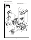
7-1 a b c d e f g h 1 2 3 4 5 6 exploded views 1 main parts section note: parts with no ref. No. In "exploded view" are not supplied. And some ref. No. Will be skipped. Be sure to make your orders of replacement parts according to the parts list. Comparison chart of models & marks model mark pv-dv10...
Page 151
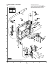
7-2 a b c d e f g h 1 2 3 4 5 6 comparison chart of models & marks model mark pv-dv100 pv-dv200 pv-dv400 pv-dv600 a b c d 2 side case l section important safety notice: components identified by the sign have special characteristics important for safety. When replacing any of these components, use on...
Page 152
7-3 a b c d e f g h 1 2 3 4 5 6 3 top case and evf section (model: a, b) important safety notice: components identified by the sign have special characteristics important for safety. When replacing any of these components, use only the specified parts. Comparison chart of models & marks model mark p...
Page 153
7-4 a b c d e f g h 1 2 3 4 5 6 3 top case and color evf section (model: c, d) important safety notice: components identified by the sign have special characteristics important for safety. When replacing any of these components, use only the specified parts. Comparison chart of models & marks model ...
Page 154
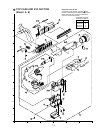
7-5 a b c d e f g h 1 2 3 4 5 6 4 lens section lubrication points lubrication points note 1 note 1 62 34 34 34 61 408 408 408 comparison chart of models & marks model mark pv-dv100 pv-dv200 pv-dv400 pv-dv600 a b c d lubrication points when the marked parts are replaced, apply the recommended lubrica...
Page 155
7-6 a b c d e f g h 1 2 3 4 5 6 5 side case r and lcd section important safety notice: components identified by the sign have special characteristics important for safety. When replacing any of these components, use only the specified parts. A 95 98 99 405 405 97 96 404 404 404 e12 404 403 94 403 73...
Page 156
7-7 a b c d e f g h 1 2 3 4 5 6 6 front case section important safety notice: components identified by the sign have special characteristics important for safety. When replacing any of these components, use only the specified parts. E38 e35 e7 e34 e33 e31 e37 e32 e36 e36 88 87 86 85 84 83 81 82 404 ...
Page 157
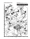
7-8 a b c d e f g h 1 2 3 4 5 6 7 mechanism section lubrication points when the marked parts are replaced, apply the recommended lubricants or adhesive for better maintenance of the unit. Mark kind of lubricant availability part number oil purchase from local supplier - - - - - - - - grease availabl...
Page 158
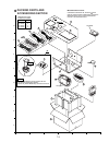
7-9 a b c d e f g h 1 2 3 4 5 6 8 packing parts and accessories section important safety notice: components identified by the sign have special characteristics important for safety. When replacing any of these components, use only the specified parts. Comparison chart of models & marks model mark pv...
Page 159: Replacement Parts Lists
8-1 replacement parts lists before replacing parts, read the following: replacement notes general notes 1. Use only original replacement parts: to maintain original function and reliability of repaired units, use only original replacement parts which are listed with their part numbers in the parts l...
Page 160
Part name remarks part no. Ref. No. Part name remarks part no. Ref. No. 8-2 mechanical replacement parts list exploded views 1 main parts section 3 403 413 413 404 403 =qm=========================bvb=`^m=rkfq ============ipvhmots========e=^i_=f===========================p ============ipvhmnus=======...
Page 161
Part name remarks part no. Ref. No. Part name remarks part no. Ref. No. 8-3 =vq=========================i`a=`^pb=^=rkfqi^_p=obpfk ============ipvhmouv========e=^=f========================== !=r ============ipvhmovm========e=_=f========================== !=r ============ipvhmovn========e=`=f=========...
Page 162
Part name remarks part no. Ref. No. Part name remarks part no. Ref. No. 8-4 service fixture and tools ============schnont=========qvb=qo^kpjfppflk=q^mb=============================sba ============scjpmnmbep======`lilo=_^o=pq^ka^oa=q^mb===========================sba ============scjpmmmbepj=====ifkb^o...
Page 163
Part name remarks part no. Ref. No. Part name remarks part no. Ref. No. 8-5 f`pmmn======qptopu_=========f`i=ildf`=sfabl=afdfq^i=pfdk^i====bkpkak ============================mol`bpp f`pmmo======_etmushs========f`i=ifkb^o=s`l f`pmmp======kgjorpusqbn=====f`i=ifkb^o=lrqmrq=aofsbo f`pomn======jkojammmmsc...
Page 164
Part name remarks part no. Ref. No. Part name remarks part no. Ref. No. 8-6 opsp========bogodbgnrnu=====jdc=`efm============nlnst==nrm opsr========bogodbmommu=====jdc=`efm============nlnst====m= opss========bogodbmommu=====jdc=`efm============nlnst====m= optm========bogodbmommu=====jdc=`efm=========...
Page 165
Part name remarks part no. Ref. No. Part name remarks part no. Ref. No. 8-7 oomnq=======bogodbgnmpu=====jdc=`efm============nlnst==nmh oomnr=======bogodbgqtqu=====jdc=`efm============nlnst=qtmh oomns=======bogodbgnmpu=====jdc=`efm============nlnst==nmh oomnt=======bogodbgnmnu=====jdc=`efm===========...
Page 166
Part name remarks part no. Ref. No. Part name remarks part no. Ref. No. 8-8 osmrp=======bogodbgqtnu=====jdc=`efm============nlnst==qtm osmrq=======bogodbgrsou=====jdc=`efm============nlnst=rksh osmrr=======bogodbgnmou=====jdc=`efm============nlnst===nh osmrs=======bogodbgnmou=====jdc=`efm===========...
Page 167
Part name remarks part no. Ref. No. Part name remarks part no. Ref. No. 8-9 `tnp========j`rsn^nmrwcs====`=`efm=====humbjomb=nms======n `tnq========b`rsn^qtrwck====`=`efm=====humbjomb=nms====qkt `tnr========b`rsn^qtrwck====`=`efm=====humbjomb=nms====qkt `nnmn=======s`rpn_^oorh_====`=`efm=============...
Page 168
Part name remarks part no. Ref. No. Part name remarks part no. Ref. No. 8-10 `qpmt=======b`pqmguqtswo====q^kq^irj=`efm=======skps====qt `qpmu=======j`rsnbnmqh_k====`=`efm==============ors====mkn `qpmv=======b`rsnbooph_s====`=`efm==============ors==mkmoo `qpnm=======b`rsnbooph_s====`=`efm============...
Page 169
Part name remarks part no. Ref. No. Part name remarks part no. Ref. No. 8-11 crystal oscillator upmn========ippummoo upomn=======spupmunm usmmn=======ippummop usmmo=======ippummps pin headers _n==========ipgmmn^cnmm_====`lkkb`qlo=nmmm _p==========sgpt_psqqm_p====`lkkb`qlo=qmm fpc connector cmn======...
Page 170
Part name remarks part no. Ref. No. Part name remarks part no. Ref. No. 8-12 npmmv=======opanpou=========`efm ============e=a=f npmno=======op^nrts^nmso====`efm ============lo=op_nonu^=====`efm ============e=a=f nqmmn=======opanpou=========`efm nqmmo=======opanpou=========`efm nqmmq=======op^nrts^nm...
Page 171
Part name remarks part no. Ref. No. Part name remarks part no. Ref. No. 8-13 oqoo========bogodbgnmnu=====jdc=`efm============nlnst==nmm oqor========bogodbmommu=====jdc=`efm============nlnst====m= oqos========bogodbgnmru=====jdc=`efm============nlnst===nj oqot========bogpdbvmomms====jdc=`efm=========...
Page 172
Part name remarks part no. Ref. No. Part name remarks part no. Ref. No. 8-14 opmov=======bogodbmommu=====jdc=`efm============nlnst====m= opmpm=======bogodbgpvou=====jdc=`efm============nlnst=pkvh opmpn=======bogodbmommu=====jdc=`efm============nlnst====m= ============e=_i`=f ============bogodbgqtou=...
Page 173
Part name remarks part no. Ref. No. Part name remarks part no. Ref. No. 8-15 osmmv=======bogodbgnmpu=====jdc=`efm============nlnst==nmh osmnm=======bogodbgnmou=====jdc=`efm============nlnst===nh osmno=======bogodbgrsou=====jdc=`efm============nlnst=rksh osmnp=======bogooearspu=====jdc=`efm===hjmkrb=...
Page 174
Part name remarks part no. Ref. No. Part name remarks part no. Ref. No. 8-16 osnvo=======bogodbmommu=====jdc=`efm============nlnst====m= ============e=`ia=f ovmmn=======bogodbmommu=====jdc=`efm============nlnst====m= ovmmo=======bogodbmommu=====jdc=`efm============nlnst====m= capacitors `pmn========...
Page 175
Part name remarks part no. Ref. No. Part name remarks part no. Ref. No. 8-17 `pmrr=======b`rbn`nmqwcn====`=`efm=====humbjomb=nss====mkn `pmrs=======b`rbnenrmg`n====`=`efm=====hjrb=====rms====nrm `pmrt=======b`rbnenmma`n====`=`efm=====hjmkrb===rms====nmm `pmru=======b`rbn`nmqwcn====`=`efm=====humbjom...
Page 176
Part name remarks part no. Ref. No. Part name remarks part no. Ref. No. 8-18 coils ipmn========sigtkvinmmhq====`efm========================nm ipmo========simmpnv^qtnq====cboofqb=_b^a=`efm ipmp========ipigce_nmmkc====`efm========================nm ipmq========ipigce_oomkc====`efm=====================...
Page 177
Part name remarks part no. Ref. No. Part name remarks part no. Ref. No. 8-19 s-jack c.B.A. Diodes aptrn=======oaskop==========wbkbo=`efm================skos aptro=======acp^skucb=======wbkbo=`efm================skus ============lo=j^wqmsuemi===wbkbo=`efm================skus aptrr=======oaskop=======...
Page 178
Part name remarks part no. Ref. No. Part name remarks part no. Ref. No. 8-20 capacitors `prmm=======b`pqmguoos======q^kq^irj=`efm=======skps====oo `prmn=======b`rsnenmpwcs====`=`efm=====humbjomb=rms===mkmn `prmp=======b`rsn^nmrh_k====`=`efm==============nms======n `prmq=======b`rsnersng`s====`=`efm=...
Page 179
Part name remarks part no. Ref. No. Part name remarks part no. Ref. No. 8-21 onmnq=======bogodbgqtou=====jdc=`efm============nlnst=qkth onmnr=======bogodbgnmou=====jdc=`efm============nlnst===nh onmns=======bogodbgnmou=====jdc=`efm============nlnst===nh onmnt=======bogodbgnmou=====jdc=`efm==========...
Page 180
Part name remarks part no. Ref. No. Part name remarks part no. Ref. No. 8-22 inmoq=======ipicmmor========bjf=cfiqbo=`efm inmor=======sigtkvinmmhq====`efm========================nm ============e=_i`ia=f inmos=======sigtkvinmmhq====`efm========================nm isrmn=======_hnsmuejnmo=====cboofqb=`lo...
Page 181
Part name remarks part no. Ref. No. Part name remarks part no. Ref. No. 8-23 capacitors `qumn=======b`rsnenmoh_s====`=`efm==============rms==nmmmm `qumo=======b`rsnenmoh_s====`=`efm==============rms==nmmmm `qump=======b`rsn`qtph_s====`=`efm==============nss==mkmqt `qumq=======b`rsn`nrph_s====`=`efm=...
Page 182
Part name remarks part no. Ref. No. Part name remarks part no. Ref. No. 8-24 resistors ovmn========bogpdbvgotms====jdc=`efm============nlnst===ot ovmo========bogpdbvgnmos====jdc=`efm============nlnst===nh ovmq========bogpdbvmomms====jdc=`efm============nlnst====m= ovmr========bogpdbvmomms====jdc=`ef...
Page 183
Part name remarks part no. Ref. No. Part name remarks part no. Ref. No. 8-25 `vot========b`rsmgqtqh_s====`=`efm==============skps==mkqt `vou========b`rsmgqtqh_s====`=`efm==============skps==mkqt coils ivmn========sinmqosgnrm=====`efm=======hjrb=============nr ivmo========sinmqosgnrm=====`efm=======h...
Page 184
Part name remarks part no. Ref. No. Part name remarks part no. Ref. No. 8-26 `umnv=======kj^mgoosjqo=====bib`qolivqf`=`efm===skps====oo `umom=======b`rsnbnmqh_k====`=`efm==============ors====mkn `umon=======s`rpg_goorh_====`=`efm==============skps===oko `umoo=======b`rsn`nmqh_s====`=`efm============...
Page 185: Ac Adaptor Section
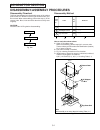
9-1 fig. Da2 disassembly/assembly procedures disassembly method disassembly flowchart this flow chart indicates the disassembly steps of the cabinet parts and the p.C. Boards in order to gain access to item (s) to be serviced. When reassembling, perform the step (s) in the reverse order. Bend, route...
Page 186: Electrical Adjustment
9-2 electrical adjustment test equipment to do reference voltage adjustments, the following equip- ments are required. 1. Dvm (digital volt metet) 2. Plastic tip driver or non-metal driver reference voltage adjustment purpose: to set the proper reference voltage output. Symptom of msadjustment: all ...
Page 187
9-3 f1001 1.6a/250v l1001 elf16m040a c1002 33/400v r1001 100k r1002 100k d1004 ma165 r1006 47 r1005 470 d1005 ma4330-h r1014 0.36 q1001 2sk2750 l1003 lslp0058 c1008 0.01 r1007 100 r1015 22 c1007 22p c1009 0.1 r1012 18k c1005 560p c1004 1000p c1003 22/50v d1003 ma4300-m r1008 220 c1010 3300p d1006 ma...
Page 188: Hot
9-4 ac adaptor c.B.A. Lsep1030a1 circuit board layout note: for schematic diagram and circuit board layout notes, refer to beginning of schematic section. Note: circuit board layout shows components installed for various models. For proper parts content for the model you are servicing, please refer ...
Page 189
9-5 ic1001 (pwm control) ic1002(error voltage det) ic1101 shunt regulator ic1102 (op. Amp) ic1104 (op. Amp) ic1103 (charge control) ic1003(error voltage det) q1001 q1101 q1102 q1104 q1105 q1103 ac adaptor c.B.A. P1001 1 p1001 2 ac in line filter osc drive pwm comparator f1001 1.6a/250v l1001 d1002 f...
Page 190: Exploded Views
9-6 a b c d e f g h 1 2 3 4 5 6 ac adaptor section note: parts with no ref. No. In "exploded view" are not supplied. And some ref. No. Will be skipped. Be sure to make your orders of replacement parts according to the parts list. 1 exploded views important safety notice: components identified by the...
Page 191
9-7 a b c d e f g h 1 2 3 4 5 6 2 packing parts and accessories section important safety notice: components identified by the sign have special characteristics important for safety. When replacing any of these components, use only the specified parts. 108 121 122 125 123 109 not supplied.
Page 192: Replacement Parts Lists
Part name remarks part no. Ref. No. Part name remarks part no. Ref. No. 9-8 replacement parts lists before replacing parts, read the following: replacement notes general notes 1. Use only original replacement parts: to maintain original function and reliability of repaired units, use only original r...
Page 193
Part name remarks part no. Ref. No. Part name remarks part no. Ref. No. 9-9 onmnp=======bogsdbvmomms====jdc=`efm============nlnmt====m= onmnq=======bouopgopsb======jbq^i=cfij==========ot====mkps onmnr=======bodopgoomb======jbq^i=lufab=========ot======oo onmns=======bogpdbvgqtms====jdc=`efm==========...
Page 194
Part name remarks part no. Ref. No. Part name remarks part no. Ref. No. 9-10 capacitors `nmmn=======b`nro^nmqjd=====mlivbpqbo==hjomb====orms===mkn= ! ============lo=b`nro^nmqjd^=mlivbpqbo==hjomb====orms===mkn= ! `nmmo=======b`^oddppmw======bib`qolivqf`========qmms====pp= ! ============lo=ip`bmmsp===...
Page 195
Printed in japan ®.

