- DL manuals
- Quectel
- Engine
- M10
- Hardware Description
Quectel M10 Hardware Description
Summary of M10
Page 1
M10 quectel cellular engine hardware design m10_hd_v1.00
Page 2
M10 hardware design document title m10 hardware design revision 1.00 date 2009-06-27 status release document control id m10_hd_v1.00 general notes quectel offers this information as a service to its customers, to support application and engineering efforts that use the products designed by quectel. ...
Page 3: Contents
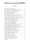
M10 hardware design contents contents ............................................................................................................................................2 0 revision history ........................................................................................................
Page 4
M10 hardware design 3.15 behaviors of the ri ..........................................................................................................51 3.16 network status indication.................................................................................................52 3.17 general pur...
Page 5: Table Index
M10 hardware design table index table 1: related documents.....................................................................................................8 table 2: terms and abbreviations .........................................................................................9 table 3: module...
Page 6: Figure Index
M10 hardware design figure index figure 1: module functional diagram .............................................................................16 figure 2: reference circuit of the vbat input ..............................................................22 figure 3: reference circuit of the sourc...
Page 7
M10 hardware design figure 40: pad bottom dimensions(unit: mm) .............................................................66 figure 41: footprint of recommendation(unit: mm)..............................................68 figure 42: top view of the module .............................................
Page 8: 0 Revision History
M10 hardware design 0 revision history revision date author description of change 1.00 2009-06-27 tracy zhang initial m10_hd_v1.00 - 7 - quectel.
Page 9: 1 Introduction
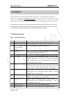
M10 hardware design 1 introduction this document defines and specifies the m10 module series. For detail product information, please refer to the chapter 6 product information.This document describes the hardware interface of the quectel’s m10 module series that connects to the specific application ...
Page 10
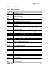
M10 hardware design 1.2 terms and abbreviations table 2: terms and abbreviations abbreviation description adc analog-to-digital converter amr adaptive multi-rate arp antenna reference point asic application specific integrated circuit ber bit error rate bts base transceiver station chap challenge ha...
Page 11
M10 hardware design abbreviation description mo mobile originated ms mobile station (gsm engine), also referred to as te mt mobile terminated pap password authentication protocol pbcch packet switched broadcast control channel pcb printed circuit board pdu protocol data unit ppp point-to-point proto...
Page 12
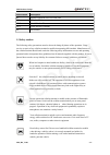
M10 hardware design abbreviation description rc mobile equipment list of received calls sm sim phonebook fwp fixed wireless phone fwt fixed wireless terminal nc not connect 1.3 safety caution the following safety precautions must be observed during all phases of the operation. Usage , service or rep...
Page 13
M10 hardware design gsm cellular terminals or mobiles operate over radio frequency signals and cellular networks and cannot be guaranteed to connect in all conditions, for example no mobile fee or a invalid sim card. While you are in this condition and need emergent help, please remember using emerg...
Page 14: 2 Product Concept
M10 hardware design 2 product concept the m10 is a quad-band gsm/gprs engine that works at frequencies gsm850, egsm 900 mhz, dcs 1800 mhz and pcs 1900 mhz. The m10 features gprs multi-slot class 12(default)/ class 10/class8 and supports the gprs coding schemes cs-1, cs-2, cs-3 and cs-4. With a tiny ...
Page 15
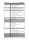
M10 hardware design z class 1 (1w) at dcs 1800 and pcs 1900 gprs connectivity z gprs multi-slot class 12 (default) z gprs multi-slot class 10 (option) z gprs multi-slot class 8 (option) z gprs mobile station class b temperature range z normal operation: -35°c ~ +80°c z restricted operation: -45°c ~ ...
Page 16
M10 hardware design 29±0.15 x 29±0.15 x 3.6±0.3mm weight: 8g firmware upgrade firmware upgrade over serial port ○ 1 when the module works in this temperature range, the deviations from the gsm specification might occur. For example, the frequency error or the phase error could increase. Table 4: cod...
Page 17
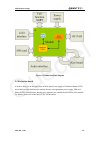
M10 hardware design figure 1 : module functional diagram 2.3 evaluation board in order to help you on the application of m10, quectel can supply an evaluation board (evb) and a link-board that interfaces the module directly with appropriate power supply, sim card holder, rs232 serial interface, hand...
Page 18: 3 Application Interface
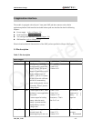
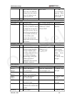
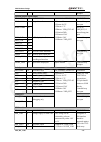
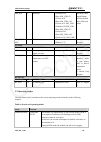
M10 hardware design 3 application interface the module is equipped with a 64-pin 1.3mm pitch smt pad that connects to the cellular application platform. Sub-interfaces included in these pads are described in detail in following chapters: z power supply (refer to chapter 3.3) z serial interfaces (ref...
Page 19
M10 hardware design judge whether the system is power on or off. When the voltage is low, the system is power off. Otherwise, the system is power on. Imax=20ma to add a 2.2~4.7uf bypass capacitor, when using this pin for power supply. Gnd digital ground power on or power off pin name i/o description...
Page 20
M10 hardware design pin open general purpose input/output pin name i/o description dc characteristics comment kbc0~kbc4 i if unused keep pins open kbr0~kbr4 o keypad interface pull up to vdd_ext, if unused keep pins open disp_data i/o disp_clk o disp_cs o disp_d/c o disp_rst o lcd display interface ...
Page 21
M10 hardware design sim_rst o sim reset volmax=0.4v when sim_vdd=3v vilmax=0.4v when sim_vdd=1.8v vilmax=0.2* sim_vdd vohmin=0.9*sim_vdd when sim_vdd=3v volmax=0.4v when sim_vdd=1.8v volmax=0.2* sim_vdd maximum cable length 200mm from the module pad to sim card holder. Sim_prese nce i sim card detec...
Page 22
M10 hardware design message and sms from the system normally. Gsm idle software is active. The module has registered to the gsm network, and the module is ready to send and receive. Gsm talk connection is going on between two subscribers. In this case, the power consumption depends on network settin...
Page 23
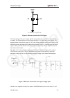
M10 hardware design c2 c1 vbat + c1=100uf, c2=0.1uf~1uf figure 2 : reference circuit of the vbat input the circuit design of the power supply depends strongly from the power source where this power is drained. The following figure is the reference design of +5v input source power supply. The designe...
Page 24
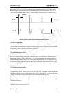
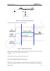
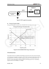
M10 hardware design time, around 577us every 4.615ms, in talking mode. The following figure is the vbat voltage and current ripple at the maximum power transmitting phase, the test condition is vbat=4.0v, vbat maximum output current =2a, c1=100µf tantalum capacitor (esr=0.7Ω) and c2=1µf. Max:400mv b...
Page 25
M10 hardware design 3.4 power up and power down scenarios 3.4.1 turn on the module can be turned on by various ways, which are described in following chapters: z via pwrkey pin: starts normal operating mode (please refer to chapter 3.4.1.1); z via rtc interrupt: starts alarm modes (please refer to c...
Page 26
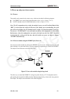
M10 hardware design s1 pwrkey tvs1 close to s1 figure 6 : turn on the module using keystroke the power on scenarios illustrates as following figure. Vdd_ext (output) v il v ih > 0.6*vbat pulldown > 2000ms hiz vbat pwrkey (input) figure 7: timing of turn on system when power on procedure complete, th...
Page 27
M10 hardware design gsm network and the software protocol stack is closed. Thus the parts of at commands related with sim card and protocol stack will not be accessible, and the others can be used as well as in normal mode. Use the “at+qalarm” command to set the alarm time. The rtc remains the alarm...
Page 28
M10 hardware design it can caused the module logoff from the network and allow the software to enter into a secure state and save data before completely disconnect the power supply. Before the completion of the switching off procedure the module will send out result code: normal power down after thi...
Page 29
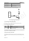
M10 hardware design following urc will be presented: under-voltage warnning if the voltage ≥ 4.5v, the following urc will be presented: over-voltage warnning the uncritical voltage range is 3.4v to 4.6v. If the voltage ≥ 4.6v or ≤ 3.4v, the module will be automatic shutdown soon. If the voltage ≤ 3....
Page 30
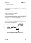
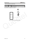
M10 hardware design s1 emerg_off tvs1 close to s1 figure 10: reference circuit for emerg_off using keystoke take care to use the emerg_off pin. It should be used under emergent situation. For instance, if the module is unresponsive or abnormal, the emerg_off pin can be used to shutdown the system, a...
Page 31
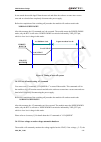
M10 hardware design pwrkey (input) pulldown > 20ms delay>2s emerg_off (input) figure 12 : timing of restart system after emergency shutdown 3.5 power saving there are two methods for the module to enter into low current consumption status. “at+cfun” is used to set module into minimum functionality m...
Page 32
M10 hardware design 3.5.2 sleep mode (slow clock mode) we can control module to enter or exit the sleep mode in customer applications through dtr signal. When dtr is in high level, and there is no on air and hardware interrupt (such as gpio interrupt or data on serial port), the module will enter sl...
Page 33
M10 hardware design 3.7 rtc backup the rtc (real time clock) power supply of module can be provided by an external capacitor or battery (rechargeable or non-chargeable) through the vrtc on the smt pad. There is a 3.9 k resistor has been integrated in the module used for limiting current. You need on...
Page 34
M10 hardware design rtc core 3.9k module vrtc large-capacitance capacitor figure 15: rtc supply from capacitor z coin-type capacitor backup coin-type rechargeable capacitor such as xh414h-iv01e form seiko can be used. Figure 16 : seiko xh414h-iv01e charge characteristic 3.8 serial interfaces the mod...
Page 35
M10 hardware design serial port z txd: send data to the rxd signal line of the dte z rxd: receive data from the txd signal line of the dte debug port z dbg_txd: send data to the /rxd signal line of the dte z dbg_rxd: receive data from the /txd signal line of the dte the logic levels are described in...
Page 36
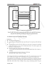
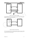
M10 hardware design txd rxd rts cts dtr dcd ri txd rxd rts cts dtr dcd /ring dbg_tx dbg_rx /txd /rxd module (dce) customer (dte) serial port1 serial port debug port serial port2 figure 17 : connection of serial interfaces note: the rts pin must be connected to the gnd in the customer circuit when on...
Page 37
M10 hardware design you the flexibility to put the gsm engine into operation no matter what baud rate your host application is configured to. To take advantage of autobauding mode, specific attention should be paid to the following requirements: synchronization between dte and dce: when dce powers o...
Page 38
M10 hardware design io connector txd rxd gnd pwrkey module(dce) serial port txd rxd gnd pwrkey figure 18 : connection of software upgrade note: the rts pin must be connected to the gnd in the customer circuit when only the txd and rxd are used in the serial port communication. Customer(dte) txd rxd ...
Page 39
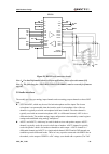
M10 hardware design 9 8 7 6 5 4 3 2 1 15 14 8 9 11 12 5 7 6 10 4 26 2 27 13 18 20 21 16 17 19 22 23 24 3 1 25 28 gnd to pc serial port sp3238 3v gnd gnd t5out /shutdown v+ gnd v- vcc t4out t2out t3out t1out r3in r2in r1in /status 3v online r1out r2out r3out /r1out gnd t5in t4in t3in t2in t1in c2+ c2...
Page 40
M10 hardware design capacitor is recommended ) which usually for block the dc voltage in the single-end mode. The module analogy output configuration is determined by control register settings and established using analogy multiplexes. Z these two analogy channels can be easily swapped by “at+qaudch...
Page 41
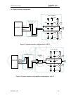
M10 hardware design 3.9.1 microphone interfaces configuration 10pf 33pf 33pf 33pf close to microphone micxp micxn gnd gnd differential layout moudle electret microphone gnd gnd 10pf 10pf gnd gnd esd anti esd anti agnd figure 21: microphone interface configuration of ain1&ain2 m10_hd_v1.00 - 40 - que...
Page 42
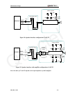
M10 hardware design 3.9.2 speaker interface configuration spk1p spk1n differential layout 10pf 10pf 33pf 33pf 33pf close to speaker gnd gnd 10pf esd anti esd anti moudle figure 22: speaker interface configuration of aout1 spk1p spk1n differential layout amplifier circuit 10pf 10pf 33pf 33pf 33pf clo...
Page 43
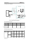
M10 hardware design spk2p agnd differential layout 10pf 33pf close to speaker gnd esd anti moudle 22uf figure 24: speaker interface configuration of aout2 spk2p agnd differential layout amplifier circuit 10pf 10pf 33pf 33pf close to speaker gnd gnd esd anti esd anti moudle c2 c1 figure 25: speaker i...
Page 44
M10 hardware design 3.9.3 earphone interface configuration 1 2 4 3 amphenol 9001-8905-050 spk2p mic2n mic2p 22uf 68r 33pf gnd gnd agnd close to socket differential layout 33pf agnd 33pf 10pf gnd gnd gnd gnd agnd moudle figure 26: earphone interface configuration table 12: mic input characteristics p...
Page 45
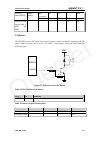
M10 hardware design load resistance 16 32 ohm auxiliary output(spk2) single ended ref level 0 2.4 vpp maxim driving current limit of spk1 and spk2 50 ma 3.10 buzzer the buzzer on the smt pads can be used to drive a buzzer to indicate incoming call. The output volume of buzzer can be set by “at+crsl”...
Page 46
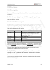
M10 hardware design 3.11 sim card interface 3.11.1 sim card application you can use at command to get information in sim card. For more information, please refer to document [1]. The sim interface supports the functionality of the gsm phase 1 specification and also supports the functionality of the ...
Page 47
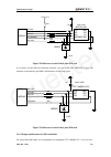
M10 hardware design module smf05c sim_vdd sim_clk sim_data sim_rst sim_presence vcc gnd rst vpp clk i/o presence gnd 100k 22r 22r 22r 1uf vdd_ext molex-91228 sim card gnd figure 28: reference circuit of the 8 pins sim card if you don’t use the sim card detection function, you can let the sim_presenc...
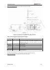
Page 48
M10 hardware design http://www.Amphenol.Com for more information about the holder. Figure 30 : amphenol c707 10m006 512 2 sim card holder table 17: pin description (amphenol sim card holder) name pin function sim_vdd c1 sim card power supply, it can identify automatically the sim card power mode,one...
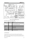
Page 49
M10 hardware design figure 31 : molex 91228 sim card holder table 18: pin description (molex sim card holder) name pin function sim_vdd c1 sim card power supply, it can identify automatically the sim card power mode,one is 3.0v±10%, another is 1.8v±10%. Current is about 10ma. Sim_rst c2 sim card res...
Page 50
M10 hardware design z supports 8-bpp (rgb332), 12-bpp (rgb444), 16-bpp (rgb565) color depths the serial lcd display interface supports serial communication with lcd device. When used as lcd interface, the following table is the pin definition. Lcd interface timing should be united with the lcd devic...
Page 51
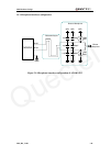
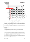
M10 hardware design kbr4 kbr3 kbr2 kbr1 kbr0 kbc0 kbc1 kbc2 kbc3 kbc4 module gpio1_kbc5 figure 32 : reference circuit of the keypad interface if 5×5 matrix couldn’t provide enough keys, gpio1 can be multiplex as kbc5 to configure a 5 × 6 matrix. And then, the keypad interface can consists of 5 keypa...
Page 52
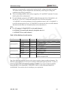
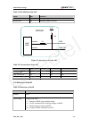
M10 hardware design table 21: pin definition of the adc name pin function adc0 41 analog to digital converter. Temp_bat 40 analog to digital converter. Base band 10k 1k 2.8v auxadc2 auxadc0 adc0 temp_bat module figure 33 : internal circuit of the adc table 22: characteristics of the adc min typ max ...
Page 53
M10 hardware design data calling change low, then: ( 1)change to high when establish calling. ( 2)use at command ath, the ri changes to high. Sms when receive sms, the ri will change to low and hold low level about 120 ms, then change to high. Urc some urcs triggers 120ms low level on ri. For more d...
Page 54
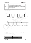
M10 hardware design 64ms on/ 800ms off the module does not find the network 64ms on/ 2000ms off the module find the network 64ms on/ 600ms off gprs communication we provide a reference circuitry for you, shown as following figure: module 300r 4.7k 47k vbat netlight figure 36 : reference circuit of t...
Page 55
M10 hardware design table 26: pin definition of the light_mos name pin function light_mos 27 open drain output port note: this function is not supported in the default firmware. There must be special firmware if you require. Please contact quectel for more details . Module 300r vbat light_mos figure...
Page 56: 4 Antenna Interface
M10 hardware design 4 antenna interface the pin 43 is the rf antenna pad. The rf interface has an impedance of 50Ω. 4.1 antenna installation m10 provides an rf antenna pad for customer’s antenna installation. The customer’s antenna should be located in the customer’s main board and connect to module...
Page 57
M10 hardware design 4.3 rf receiving sensitivity table 29: the module conducted rf receiving sensitivity frequency receive sensitivity gsm850 egsm900 dcs1800 -107dbm pcs1900 -107dbm 4.4 operating frequencies table 30: the module operating frequencies frequency receive transmitting channel gsm850 869...
Page 58
M10 hardware design 5 electrical, reliability and radio characteristics 5.1 pin assignment of the module notes: be careful, the connection diagrams adapt to only right module, please check your module type. M10_hd_v1.00 - 57 - quectel.
Page 59
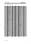
M10 hardware design table 31: m10 connection diagrams pin no. Pin name i/o pin no. Pin name i/o 1 disp_data i/o 2 disp_clk o 3 disp_cs o 4 disp_d/c o 5 disp_rst o 6 netlight o 7 vdd_ext o 8 gnd1 9 dbg_rxd i 10 dbg_txd o 11 sim_presence i 12 sim_vdd o 13 sim_data i/o 14 sim_clk o 15 sim_rst o 16 vrtc...
Page 60
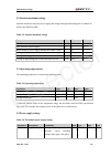
M10 hardware design 5.2 absolute maximum ratings absolute maximum rating for power supply and voltage on digital and analog pins of module are listed in the following table: table 32: absolute maximum ratings parameter min max unit vbat 0 4.7 v peak current of power supply 0 3 a rms current of power...
Page 61
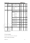
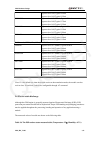
M10 hardware design voltage drop during transmitting burst normal condition, power control level for pout max 400 mv voltage ripple normal condition, power control level for pout max @ f @ f>200khz 50 2 mv power down mode sleep mode @ drx=5 65 1.1 ua ma minimum functionality mode at+cfun=0 idle mode...
Page 62
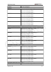
M10 hardware design condition current consumption voice call gsm850 @power level #5 @power level #10,typical 150ma @power level #19,typical 100ma egsm 900 @power level #5 @power level #10,typical 140ma @power level #19,typical 100ma dcs 1800 @power level #0 @power level #10,typical 150ma @power leve...
Page 63
M10 hardware design @power level #10,typical 182ma @power level #19,typical 125ma egsm 900 @power level #5 @power level #10,typical 175ma @power level #19,typical 125ma dcs 1800 @power level #0 @power level #10,typical 135ma @power level #15,typical 120ma pcs 1900 @power level #0 @power level #10,ty...
Page 64
M10 hardware design part contact discharge air discharge vbat,gnd ±5kv ±10kv pwrkey ±4kv ±8kv antenna port ±5kv ±10kv spk1p/1n, spk2p/2n, mic1p/1n, mic2p/2n ±4kv ±8kv m10_hd_v1.00 - 63 - quectel.
Page 65: 6 Product Information
M10 hardware design 6 product information table 37: ordering information part number m10 frequency bands(mhz) gsm850 egsm900 dcs1800 pcs1900 rf function gsm/gprs m10_hd_v1.00 - 64 - quectel.
Page 66: 7 Mechanics
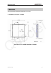
M10 hardware design 7 mechanics this chapter describes the mechanical dimensions of the module. 7.1 mechanical dimensions of module figure 38: m10 top and side dimensions(unit: mm) m10_hd_v1.00 - 65 - quectel.
Page 67
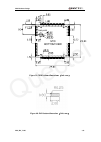
M10 hardware design m10 bottom view test point figure 39: m10 bottom dimensions (unit: mm) figure 40: pad bottom dimensions(unit: mm) m10_hd_v1.00 - 66 - quectel.
Page 68
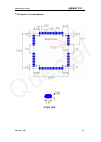
M10 hardware design 7.2 footprint of recommendation single pad m10_hd_v1.00 - 67 - quectel.
Page 69
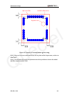
M10 hardware design keepout area module dimension safe area line figure 41: footprint of recommendation(unit: mm) note1 : keep out on the user mainboard below the test point and the keepout area ,as these are solder mask. Note2 : for maintain this module, the placement must be keep a distance betwee...
Page 70
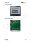
M10 hardware design 7.3 top view of the module figure 42 : top view of the module 7.4 bottom view of the module figure 43 : bottom view of the module m10_hd_v1.00 - 69 - quectel.
Page 71
Shanghai quectel wireless solutions co., ltd. Room 801, building e, no.1618, yishan road, shanghai, china 201103 tel: +86 21 5108 2965 mail: info@quectel.Com.

