Preliminary data this is preliminary information on a new product now in development or undergoing evaluation. Details are subject to change without notice. July 2007 rev 2 1/67 1 stm32f103x6 stm32f103x8 stm32f103xb performance line, arm-based 32-bit mcu with flash, usb, can, seven 16-bit timers, tw...
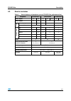
Stm32f103xx description 7/67 2.1 device overview table 2. Device features and peripheral counts (stm32f103xx performance line) peripheral stm32f103cx stm32f103rx stm32f103vx flash - kbytes 32 64 32 64 128 64 128 sram - kbytes 10 20 10 20 20 ti mer s general purpose 2 3 2 3 3 advanced control 1 1 1 c...
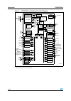
Description stm32f103xx 14/67 figure 1. Stm32f103xx performance line block diagram 1. T a = –40 °c to +105 °c (junction temperature up to 125 °c). 2. Af = alternate function on i/o port pin. Usbdp/cantx pa[15:0] exti w w d g 12bit adc1 jtag & swd 16af jtdi jtck/swclk jtms/swdio jntrst jtdo nrst v dd...
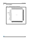
Stm32f103xx pin descriptions 15/67 3 pin descriptions figure 2. Stm32f103xx performance line lqfp100 pinout 100 99 98 97 96 95 94 93 92 91 90 89 88 87 86 85 84 83 82 81 80 79 78 77 76 1 2 3 4 5 6 7 8 9 10 11 12 13 14 15 16 17 18 19 20 21 22 23 24 25 75 74 73 72 71 70 69 68 67 66 65 64 63 62 61 60 59...
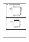
Pin descriptions stm32f103xx 16/67 figure 3. Stm32f103xx performance line lqfp64 pinout figure 4. Stm32f103xx performance line lqfp48 pinout 64 63 62 61 60 59 58 57 56 55 54 53 52 51 50 49 48 47 46 45 44 43 42 41 40 39 38 37 36 35 34 33 17 18 19 20 21 22 23 24 29 30 31 32 25 26 27 28 1 2 3 4 5 6 7 8...
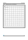
Stm32f103xx pin descriptions 17/67 figure 5. Stm32f103xx performance line bga100 ballout ai16001 pe10 pc14- osc32_in pc5 pa5 pc3 pb4 pe15 pb2 pc4 pa4 h pe14 pe11 pe7 d pd4 pd3 pb8 pe3 c pd0 pc12 pe5 pb5 pc0 pe2 b pc11 pd2 pc15- osc32_out pb7 pb6 a 8 7 6 5 4 3 2 1 vss_5 osc_in osc_out vdd_5 g f e pc1...
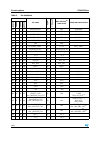
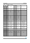
Pin descriptions stm32f103xx 18/67 table 3. Pin definitions pins pin name ty p e (1) i / o l e vel (2 ) main function (3) (after reset) default alternate functions bga1 00 lq fp4 8 lq fp6 4 lq fp100 a3 - - 1 pe2/traceck i/o ft pe2 traceck b3 - - 2 pe3/traced0 i/o ft pe3 traced0 c3 - - 3 pe4/traced1 ...
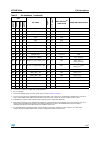
Stm32f103xx pin descriptions 19/67 g3 14 20 29 pa4/spi1_nss/ usart2_ck/adc_in4 i/o pa4 spi1_nss (6) / usart2_ck (6) / adc_in4 h3 15 21 30 pa5/spi1_sck/ adc_in5 i/o pa5 spi1_sck (6) / adc_in5 j3 16 22 31 pa6/spi1_miso/ adc_in6/tim3_ch1 i/o pa6 spi1_miso (6) / adc_in6/tim3_ch1 (6) k3 17 23 32 pa7/spi1...
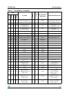
Pin descriptions stm32f103xx 20/67 g8 28 36 54 pb15/spi2_mosi tim1_ch3n i/o ft pb15 spi2_mosi (5) / tim1_ch3n (6) k9 - - 55 pd8 i/o ft pd8 j9 - - 56 pd9 i/o ft pd9 h9 - - 57 pd10 i/o ft pd10 g9 - - 58 pd11 i/o ft pd11 k10 - - 59 pd12 i/o ft pd12 j10 - - 60 pd13 i/o ft pd13 h10 - - 61 pd14 i/o ft pd1...
Stm32f103xx pin descriptions 21/67 d8 5 5 81 pd0 i/o ft osc_in (7) e8 6 6 82 pd1 i/o ft osc_out (7) b7 54 83 pd2/tim3_etr i/o ft pd2 tim3_etr c7 - - 84 pd3 i/o ft pd3 d7 - - 85 pd4 i/o ft pd4 b6 - - 86 pd5 i/o ft pd5 c6 - - 87 pd6 i/o ft pd6 d6 - - 88 pd7 i/o ft pd7 a7 39 55 89 pb3/jtdo/traceswo i/o...
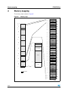
Memory mapping stm32f103xx 22/67 4 memory mapping the memory map is shown in figure 6 . Figure 6. Memory map reserved 1 kbit 0x4000 0000 0x4000 0400 0x4000 0800 0x4000 0c00 0x4000 2800 0x4000 2c00 0x4000 3000 0x4000 3400 0x4000 3800 0x4000 3c00 0x4000 4400 0x4000 4800 0x4000 4c00 0x4001 0c00 0x4001 ...
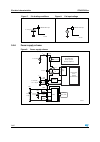
Electrical characteristics stm32f103xx 24/67 5.1.6 power supply scheme figure 9. Power supply scheme figure 7. Pin loading conditions figure 8. Pin input voltage ai14141 c = 50 pf stm32f103xx pin ai14142 stm32f103xx pin vin ai14125 3.3v vdd 1/2/3/4/5 analog: rcs, pll, ... Po wer swi tch vbat 3.3 v g...
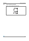
Stm32f103xx electrical characteristics 25/67 5.1.7 current consumption measurement figure 10. Current consumption measurement scheme ai14126 vbat vdd vdda idd_vbat idd.
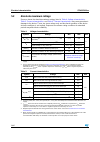
Electrical characteristics stm32f103xx 26/67 5.2 absolute maximum ratings stresses above the absolute maximum ratings listed in table 4: voltage characteristics , table 5: current characteristics , and table 6: thermal characteristics may cause permanent damage to the device. These are stress rating...
Stm32f103xx electrical characteristics 27/67 5.3 operating conditions 5.3.1 general operating conditions 5.3.2 operating conditions at power-up / power-down the parameters given in table 8 are derived from tests performed under the ambient temperature condition summarized in table 7 . Table 8. Opera...
Electrical characteristics stm32f103xx 28/67 5.3.3 embedded reset and power control block characteristics the parameters given in table 9 are derived from tests performed under ambient temperature and v dd supply voltage conditions summarized in table 7 . 5.3.4 embedded reference voltage the paramet...
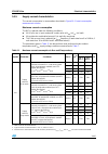
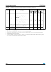
Stm32f103xx electrical characteristics 29/67 5.3.5 supply current characteristics the current consumption is measured as described in figure 10: current consumption measurement scheme . Maximum current consumption the mcu is placed under the following conditions: ● all i/o pins are in input mode wit...
Electrical characteristics stm32f103xx 30/67 table 12. Maximum current consumption in stop and standby modes (1) symbol parameter conditions typ (2) max (3) unit v dd / v bat = 2.4 v v dd /v bat = 3.3 v t a = 85 °c t a = 105 °c i dd supply current in stop mode regulator in run mode, low-speed and hi...
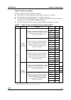
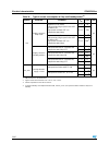
Stm32f103xx electrical characteristics 31/67 typical current consumption the mcu is placed under the following conditions: ● all i/o pins are in input mode with a static value at v dd or v ss (no load). ● all peripherals are disabled except if it is explicitly mentioned. ● the flash access time is a...
Electrical characteristics stm32f103xx 32/67 table 14. Typical current consumption in stop and standby modes (1) symbol parameter conditions v dd typ (2) unit i dd supply current in stop mode regulator in run mode, low-speed and high-speed internal rc oscillators off high-speed oscillator off (no in...
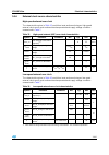
Stm32f103xx electrical characteristics 33/67 5.3.6 external clock source characteristics high-speed external user clock the characteristics given in table 15 result from tests performed using an high-speed external clock source, and under ambient temperature and supply voltage conditions summarized ...
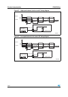
Electrical characteristics stm32f103xx 34/67 figure 11. High-speed external clock source ac timing diagram figure 12. Low-speed external clock source ac timing diagram ai14143 osc _in exter nal stm32f103xx clock sourc e vhseh tf(hse) tw(hse) il 90% 10% thse t tr(hse) tw(hse) fhse_ext vhsel ai14144b ...
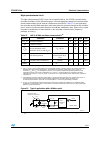
Stm32f103xx electrical characteristics 35/67 high-speed external clock the high-speed external (hse) clock can be supplied with a 4 to 16 mhz crystal/ceramic resonator oscillator. All the information given in this paragraph are based on characterization results obtained with typical external compone...
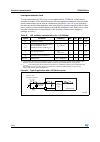
Electrical characteristics stm32f103xx 36/67 low-speed external clock the low-speed external (lse) clock can be supplied with a 32.768 khz crystal/ceramic resonator oscillator. All the information given in this paragraph are based on characterization results obtained with typical external components...
Stm32f103xx electrical characteristics 37/67 5.3.7 internal clock source characteristics the parameters given in table 19 are derived from tests performed under ambient temperature and v dd supply voltage conditions summarized in table 7 . High-speed internal (hsi) rc oscillator lsi low speed intern...
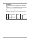
Electrical characteristics stm32f103xx 38/67 wakeup time from low power mode the wakeup times given in table 21 is measured on a wakeup phase with a 8-mhz hsi rc oscillator. The clock source used to wake up the device depends from the current operating mode: ● stop or standby mode: the clock source ...
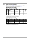
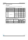
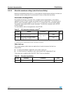
Stm32f103xx electrical characteristics 39/67 5.3.9 memory characteristics flash memory the characteristics are given at t a = − 40 to 105 °c unless otherwise specified. Table 24. Flash memory endurance and data retention table 23. Flash memory characteristics symbol parameter conditions min typ max ...
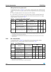
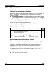
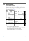
Electrical characteristics stm32f103xx 40/67 5.3.10 emc characteristics susceptibility tests are performed on a sample basis during device characterization. Functional ems (electromagnetic susceptibility) while a simple application is executed on the device (toggling 2 leds through i/o ports). The d...
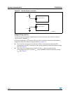
Stm32f103xx electrical characteristics 41/67 prequalification trials most of the common failures (unexpected reset and program counter corruption) can be reproduced by manually forcing a low state on the nrst pin or the oscillator pins for 1 second. To complete these trials, esd stress can be applie...
Electrical characteristics stm32f103xx 42/67 5.3.11 absolute maximum ratings (electrical sensitivity) based on three different tests (esd, lu) using specific measurement methods, the device is stressed in order to determine its performance in terms of electrical sensitivity. Electrostatic discharge ...
Stm32f103xx electrical characteristics 43/67 5.3.12 i/o port pin characteristics general input/output characteristics unless otherwise specified, the parameters given in table 29 are derived from tests performed under ambient temperature and v dd supply voltage conditions summarized in table 7 . All...
Electrical characteristics stm32f103xx 44/67 figure 15. Unused i/o pin connection output driving current the gpios (general purpose input/outputs) can sink or source up to +/-8 ma, and sink +20 ma (with a relaxed v ol ). In the user application, the number of i/o pins which can drive current must be...
Stm32f103xx electrical characteristics 45/67 output voltage levels unless otherwise specified, the parameters given in table 30 are derived from tests performed under ambient temperature and v dd supply voltage conditions summarized in table 7 . Table 30. Output voltage characteristics symbol parame...
Electrical characteristics stm32f103xx 46/67 input/output ac characteristics the definition and values of input/output ac characteristics are given in figure 16 and table 31 , respectively. Unless otherwise specified, the parameters given in table 31 are derived from tests performed under ambient te...
Stm32f103xx electrical characteristics 47/67 figure 16. I/o ac characteristics definition 5.3.13 nrst pin characteristics the nrst pin input driver uses cmos technology. It is connected to a permanent pull-up resistor, r pu (see table 29 ). Unless otherwise specified, the parameters given in table 3...
Electrical characteristics stm32f103xx 48/67 figure 17. Recommended nrst pin protection 2. The reset network protects the device against parasitic resets. 3. The user must ensure that the level on the nrst pin can go below the v il(nrst) max level specified in table 32 . Otherwise the reset will not...
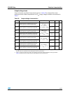
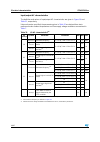
Stm32f103xx electrical characteristics 49/67 5.3.15 communications interfaces i 2 c interface characteristics unless otherwise specified, the parameters given in table 34 are derived from tests performed under ambient temperature, f pclk1 frequency and v dd supply voltage conditions summarized in ta...
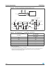
Electrical characteristics stm32f103xx 50/67 figure 18. I 2 c bus ac waveforms and measurement circuit 1. Measurement points are done at cmos levels: 0.3v dd and 0.7v dd . Table 35. Scl frequency (f pclk1 = 36 mhz.,v dd = 3.3 v) (1)(2)(3) 1. Tbd = to be determined. 2. R p = external pull-up resistan...
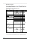
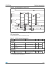
Stm32f103xx electrical characteristics 51/67 spi interface characteristics unless otherwise specified, the parameters given in table 36 are derived from tests performed under ambient temperature, f pclkx frequency and v dd supply voltage conditions summarized in table 7 . Refer to section 5.3.12: i/...
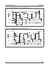
Electrical characteristics stm32f103xx 52/67 figure 19. Spi timing diagram - slave mode and cpha = 0 1. Measurement points are done at cmos levels: 0.3v dd and 0.7v dd . Figure 20. Spi timing diagram - slave mode and cpha = 1 1) ai14134 sck input cpha= 0 mosi i nput miso out p ut cpha= 0 ms b o ut m...
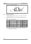
Stm32f103xx electrical characteristics 53/67 figure 21. Spi timing diagram - master mode 1. Measurement points are done at cmos levels: 0.3v dd and 0.7v dd . Usb characteristics the usb interface is usb-if certified (full speed). Table 37. Usb dc electrical characteristics symbol parameter condition...
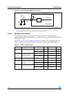
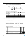
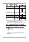
Electrical characteristics stm32f103xx 54/67 figure 22. Usb timings: definition of data signal rise and fall time 5.3.16 can (controller area network) interface refer to i/o port characteristics for more details on the input/output alternate function char- acteristics (cantx and canrx). 5.3.17 12-bi...
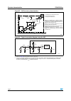
Electrical characteristics stm32f103xx 56/67 figure 23. Adc accuracy characteristics figure 24. Typical connection diagram using the adc 1. Refer to table 39 for the values of r adc and c adc . 2. C parasitic must be added to c ain . It represents the capacitance of the pcb (dependent on soldering a...
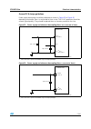
Stm32f103xx electrical characteristics 57/67 general pcb design guidelines power supply decoupling should be performed as shown in figure 25 or figure 26 , depending on whether v ref+ is connected to v dda or not. The 10 nf capacitors should be ceramic (good quality). They should be placed them as c...
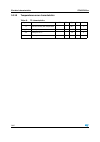
Electrical characteristics stm32f103xx 58/67 5.3.18 temperature sensor characteristics table 41. Ts characteristics symbol parameter conditions min typ max unit t l v sense linearity with temperature ± 1.5 °c avg_slope average slope 4.478 mv/°c v 25 voltage at 25 °c 1.4 v t start startup time 4 10 µ...
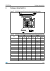
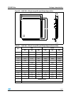
Stm32f103xx package characteristics 59/67 6 package characteristics figure 27. Lfbga100 - low profile fine pitch ball grid array package outline table 42. Lfbga100 - low profile fine pitch ball grid array package mechanical data dim. Mm inches min typ max min typ max a 1.700 0.067 a1 0.270 0.011 a2 ...
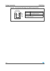
Package characteristics stm32f103xx 60/67 figure 28. Recommended pcb design rules (0.80/0.75 mm pitch bga) dpad dsm dpad 0.37 mm dsm 0.52 mm typ. (depends on solder mask registration tolerance solder paste 0.37 mm aperture diameter – non solder mask defined pads are recommended – 4 to 6 mils screen ...
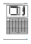
Stm32f103xx package characteristics 61/67 figure 29. Lqfp100 – 100-pin low-profile quad flat package outline table 43. Lqfp100 – 100-pin low-profile quad flat package mechanical data dim. Mm inches min typ max min typ max a 1.60 0.063 a1 0.05 0.15 0.002 0.006 a2 1.35 1.40 1.45 0.053 0.055 0.057 b 0....
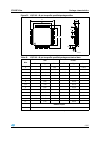
Package characteristics stm32f103xx 62/67 figure 30. Lqfp64 – 64 pin low-profile quad flat package outline table 44. Lqfp64 – 64 pin low-profile quad flat package mechanical data dim. Mm inches min typ max min typ max a 1.60 0.063 a1 0.05 0.15 0.002 0.006 a2 1.35 1.40 1.45 0.053 0.055 0.057 b 0.17 0...
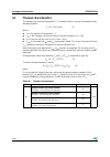
Stm32f103xx package characteristics 63/67 figure 31. Lqfp48 – 48 pin low-profile quad flat package outline table 45. Lqfp48 – 48 pin low-profile quad flat package mechanical data dim. Mm inches (1) 1. Values in inches are converted from mm and rounded to 3 decimal digits. Min typ max min typ max a 1...
Package characteristics stm32f103xx 64/67 6.1 thermal characteristics the average chip-junction temperature, t j , in degrees celsius, may be calculated using the following equation: t j = t a + (p d x Θ ja ) (1) where: ● t a is the ambient temperature in ° c, ● Θ ja is the package junction-to-ambie...
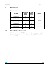
Stm32f103xx order codes 65/67 7 order codes 7.1 future family enhancements further developments of the stm32f103xx performance line will see an expansion of the current options. Larger packages will soon be available with up to 512kb flash, 64kb sram and with extended features such as emi support, s...

