- DL manuals
- SV2000
- DVD VCR Combo
- CWV20V6
- Service Manual
SV2000 CWV20V6 Service Manual
SERVICE MANUAL
Main Section
I
Specifications
I
Preparation for Servicing
I
Adjustment Procedures
I
Schematic Diagrams
I
CBA’s
I
Exploded Views
I
Parts List
When servicing the deck
mechanism, refer to MK14 Deck
Mechanism Section.
Deck Mechanism Part No.:
N2460FL
DVD RECORDER &
VIDEO CASSETTE RECORDER
CWV20V6
STANDBY-ON
REW
F.FWD
STOP/EJECT
PLAY
RECORD
CHANNEL
D.DUBBING
OPEN/CLOSE
SOURCE
VCR
DVD
S-VIDEO
VIDEO
AUDIO
L
R
SELECT
STOP
PLAY
RECORD
VCR REC
D.DUBBING
VCR DVD
TIMER REC
DVD REC
Summary of CWV20V6
Page 1
Service manual main section i specifications i preparation for servicing i adjustment procedures i schematic diagrams i cba’s i exploded views i parts list when servicing the deck mechanism, refer to mk14 deck mechanism section. Deck mechanism part no.: n2460fl dvd recorder & video cassette recorder...
Page 2: Important Safety Notice
Important safety notice proper service and repair is important to the safe, reliable operation of all funai equipment. The service procedures recommended by funai and described in this service manual are effective methods of performing service operations. Some of these service special tools should b...
Page 3: Main Section
Main section dvd recorder & video cassette recorder cwv20v6 table of contents specifications . . . . . . . . . . . . . . . . . . . . . . . . . . . . . . . . . . . . . . . . . . . . . . . . . . . . . . . . . . . . . . . . . . . . . . . . . . 1-1-1 laser beam safety precautions . . . . . . . . . . . ....
Page 4: Specifications
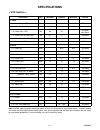
1-1-1 e9400sp specifications note: nominal specs represent the design specs. All units should be able to approximate these – some will exceed and some may drop slightly below these specs. Limit specs represent the absolute worst condition that still might be considered acceptable; in no case should ...
Page 5
1-1-2 e9400sp notes: 1. All items are measured without pre-emphasis unless otherwise specified. 2. Power supply : ac120 v 60 hz 4. Ambient temperature : 5 ° c ~ 40 ° c item conditions unit nominal limit 1. Video 1-1. Video output 75 ohm load vp-p 1.0 1-2. S-video output y (luminance) 75 ohm load vp-...
Page 6
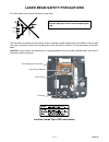
1-2-1 r3nlsp laser beam safety precautions this dvd player uses a pickup that emits a laser beam. The laser beam is emitted from the location shown in the figure. When checking the laser diode, be sure to keep your eyes at least 30 cm away from the pickup lens when the diode is turned on. Do not loo...
Page 7: Important Safety Precautions
1-3-1 dvdn_isp important safety precautions product safety notice some electrical and mechanical parts have special safety-related characteristics which are often not evident from visual inspection, nor can the protection they give necessarily be obtained by replacing them with components rated for ...
Page 8
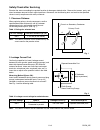
1-3-2 dvdn_isp safety check after servicing examine the area surrounding the repaired location for damage or deterioration. Observe that screws, parts, and wires have been returned to their original positions. Afterwards, do the following tests and confirm the specified values to verify compliance w...
Page 9: Standard Notes For Servicing
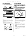
1-4-1 dvdn_sn standard notes for servicing circuit board indications 1. The output pin of the 3 pin regulator ics is indicated as shown. 2. For other ics, pin 1 and every fifth pin are indicated as shown. 3. The 1st pin of every male connector is indicated as shown. Instructions for connectors 1. Wh...
Page 10
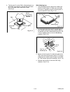
1-4-2 dvdn_sn 3. The flat pack-ic on the cba is affixed with glue, so be careful not to break or damage the foil of each pin or the solder lands under the ic when removing it. With soldering iron: 1. Using desoldering braid, remove the solder from all pins of the flat pack-ic. When you use solder fl...
Page 11
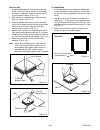
1-4-3 dvdn_sn with iron wire: 1. Using desoldering braid, remove the solder from all pins of the flat pack-ic. When you use solder flux which is applied to all pins of the flat pack-ic, you can remove it easily. (fig. S-1-3) 2. Affix the wire to a workbench or solid mounting point, as shown in fig. ...
Page 12
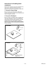
1-4-4 dvdn_sn instructions for handling semi- conductors electrostatic breakdown of the semi-conductors may occur due to a potential difference caused by electrostatic charge during unpacking or repair work. 1. Ground for human body be sure to wear a grounding band (1 m Ω) that is properly grounded ...
Page 13: Preparation For Servicing
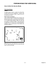
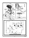
1-5-1 e9a80pfs preparation for servicing how to enter the service mode about optical sensors caution: an optical sensor system is used for the tape start and end sensors on this equipment. Carefully read and follow the instructions below. Otherwise the unit may operate erratically. What to do for pr...
Page 14
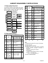
1-6-1 e9ab1dc cabinet disassembly instructions 1. Disassembly flowchart this flowchart indicates the disassembly steps to gain access to item(s) to be serviced. When reassembling, follow the steps in reverse order. Bend, route, and dress the cables as they were originally. 2. Disassembly method note...
Page 15
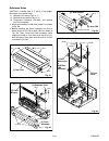
1-6-2 e9ab1dc reference notes caution 1: locking tabs (l-1) and (l-2) are fragile. Be careful not to break them. 1-1. Release five locking tabs (l-1). 1-2. Release three locking tabs (l-2) 1-3. Disconnect connector (cn1609), and remove the front assembly. 2. When reassembling, solder wire jumpers as...
Page 16
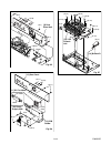
1-6-3 e9ab1dc fig. D5 (s-6) (s-7) (s-7) (s-7) cn102 cn101 (s-8) [9] rear panel unit fig. D6 (s-11) (s-11) (s-9) (s-9) ac cord earth plate hook (s-9) (s-10) [13] rear panel [10] power supply cba [12] pcb holder [11] dc fan motor fig. D7 (s-13) (s-13) (s-13) (s-14) (s-14) (s-15) (s-16) (s-14) (s-14) (...
Page 17
1-6-4 e9ab1dc [19] main cba [16] deck assembly [17] power sw cba [18] dvd open /close sw cba fe head cylinder assembly ace head assembly desolder lead with blue stripe desolder lead with blue stripe [19] main cba sw512 ld-sw from fe head bottom view lead connections of deck assembly and main cba des...
Page 18
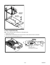
1-6-5 e9ab1dc 3. How to eject manually note: when rotating the gear, be careful not to damage the gear. 1. Remove the top cover. 2. Rotate the gear in the direction of the arrow manually as shown below until the tray descends. 3. Pull the tray out manually and remove a disc. Fig. D9 [20] deck pedest...
Page 19
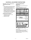
1-7-1 h9801ea electrical adjustment instructions general note: “cba” is abbreviation for “circuit board assembly.” note: 1. Electrical adjustments are required after replacing circuit components and certain mechanical parts. It is important to do these adjustments only after all repairs and replacem...
Page 20
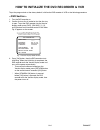
1-8-1 e9a80int how to initialize the dvd recorder & vcr to put the program back at the factory-default, initialize the dvd recorder & vcr as the following procedure. 1. Turn the dvd recorder on. 2. Confirm that no disc is loaded or that the disc tray is open. To put the dvd recorder into the version...
Page 21: Firmware Renewal Mode
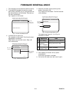
1-9-1 e9ab0fw firmware renewal mode 1. Turn the power on and remove the disc on the tray. 2. To put the dvd recorder into version up mode, press [dvd], [cm skip], [6], [5], and [4] buttons on the remote control unit in the order. Then the tray will open automatically. Fig. A appears on the screen. 3...
Page 22: Function Indicator Symbols
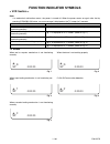
1-10-1 e9a12fis function indicator symbols note: if a mechanical malfunction occurs, the power is turned off. When the power comes on again after that by pressing [standby-on] button, an error message is displayed on the tv screen for 5 seconds. Tv screen when reel or capstan mechanism is not functi...
Page 23
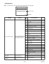
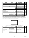
1-10-2 e9a12fis note: if an error occurs, a message with the error number appears on the screen. Message solution error no. Error description priority can not record on this disc. Insert the recordable disc, and ensure the disc status satisfies the recording requirements. 1 an error occurs during da...
Page 24
1-10-3 e9a12fis if an error occurs during the timer recording, one of the following error numbers (40 to 42) or the above error messages (error number: 1 to 46) is displayed on the recording menu after timer recording. (once the timer programming list with error indication is displayed, the program ...
Page 25: Block Diagrams
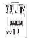
1-11-1 block diagrams system control block diagram e9ab1bls 86 key- 2 key- 1 s-data-out sys-reset s-data-in s-clk ready/busy po wer cn2212 cn2211 d561 po wer sw601 key switch (vcr) key switch (dvd) tp502 s-inh 44 power-sw 11 al+5v 22 power-led power sw cba dvd open/close sw cba cn2210 cn2209 open/cl...
Page 26
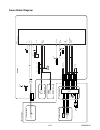
1-11-2 servo block diagram e9ab1blsv sensor cba sensor cba contr ol head cl504 cn502 cn504 ac head assembly c-fg c-cont d-pfg st-s t-reel c-f/r ctl(+) rec- saf-sw pg-delay end-s ic501 (servo control) 65 74 ctl 76 ctl(-) 75 33 67 88 81 3 32 84 22 lm-fwd/rev 26 d-cont 34 (deck assembly) end-s t-reel t...
Page 27
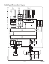
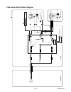
1-11-3 digital signal process block diagram e9ab1bld ic101 fr ont -end digit a l signal pr ocess ic201 rf/ err or amp ic301 m oto r driver m oto r driver ic202 op amp ic302 ic104 (flash memor y) d vd main cb a t o video output select block dia g ram t o video input select block dia g ram t o a udio ...
Page 28
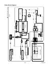
1-11-4 video block diagram e9ab1blv main cb a rec video signal pb video signal osd character mix 47 49 ic501 (osd) luminance signal process video (r)-1 head video (l)-1 head (deck assembly) cn253 1 2 3 4 5 6 video agc rp r p sync sepa fbc y/c mix ccd 1h delay r p ynr/comb filter chrominance signal p...
Page 29
1-11-5 video input select block diagram e9ab1blvis t o digit a l signal pr ocess block dia gram rec video signal main cb a 22 y -in2 11 c-in2 44 video-in2 (video input select) ic805 jk1401 s-video in 3 4 2 1 y y1 video1 video2 tu-video mute mute mute y2 c1 c2 c video - in1 jk804 tu900 (tuner unit) j...
Page 30
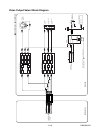
1-11-6 video output select block diagram e9ab1blvos d vd main cb a main cb a cn701 24 24 video-y(i/p)-out 22 22 video-c-out 28 28 video-cb/pb-out 26 26 video-cr/pr-out video-y(i/p) video-c video-cb/pb video-cr/pr jk1402 s-video out cn201 3 4 2 1 ic1405 (video driver) 4db amp 2db amp lpf driver yc ic...
Page 31
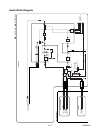
1-11-7 audio block diagram e9ab1bla rec amp serial i/f 9 8 au t o bias 11 p-on+5v p-on+5v q421 bias osc q422 q426 (pb=on) q425 switching d-rec off 6 eq amp line amp mute lpf 10 sp/lp-on p r alc (a udio pr ocess) 76 80 78 tuner line 1 line 2 4 a udio-pb/rec cn504 3a udio -com 1 ae-h 2 ae-h/fe-h a udi...
Page 32
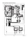
1-11-8 e9ab1blas audio input/output select block diagram digit a l a udio out (co a x1al) d v d-a udio-mute output -select jk1202 jk805 amp q1351 q804 q 806 a u dio(l) -out1 main cb a fr ont j a ck cb a a u dio(r) -out1 jk801 a udio(l) -in2 a udio(r) -in2 jk800 jk804 a udio(l) -in1 a udio(r) -in1 si...
Page 33
1-11-9 e9ab1blh hi-fi audio block diagram 57 48 47 13 14 69 71 6 7 9 r-ch insel l-ch insel nor sw serial data decoder output select vco lpf l-ch bpf r-ch pnr pilot det cont stereo pll stereo filter sap filter sap det sif demod sap demod l-r demod st/sap sw matrix l-ch pnr lim dev comp sw noise vco l...
Page 34: Hot
1-11-10 e9ab1blp power supply block diagram a v ac1001 f1001 1a 250v line filter l1001 d1001 - d1004 bridge rectifier 2 4 q1001 q1003 q1008 8 7 3 4 ic010 error voltage det hot cold t001 q055 q052 q102 q103 power supply cba main cba junction cba f hot circuit. Be careful. 20 19 18 17 16 15 14 13 12 1...
Page 35
1-12-1 d6n_sc schematic diagrams / cba’s and test points standard notes warning many electrical and mechanical parts in this chassis have special characteristics. These characteristics often pass unnoticed and the protection afforded by them cannot necessarily be obtained by using replacement compon...
Page 36
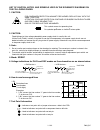
1-12-2 d6n_sc list of caution, notes, and symbols used in the schematic diagrams on the following pages: 1. Caution: for continued protection against fire hazard, replace only with the same type fuse. Attention: pour une protection continue les risqes d'incele n'utiliser que des fusible de mÊme type...
Page 37
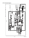
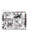
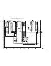
1-12-3 main 1/7 schematic diagram e9ab1scm1.
Page 38
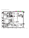
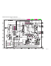
1-12-4 main 2/7, power sw, dvd open/close sw & sensor schematic diagram e9ab1scm2.
Page 39
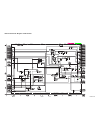
1-12-5 main 3/7 schematic diagram e9ab1scm3.
Page 40
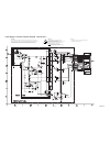
1-12-6 main 4/7 schematic diagram e9ab1scm4.
Page 41
1-12-7 main 5/7 schematic diagram e9ab1scm5.
Page 42
1-12-8 main 6/7 schematic diagram e9ab1scm6.
Page 43
1-12-9 main 7/7 schematic diagram e9ab1scm7.
Page 44
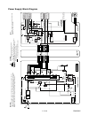
1-12-10 power supply & junction schematic diagram e9ab1scp caution ! Fixed voltage (or auto voltage selectable) power supply circuit is used in this unit. If main fuse (f1001) is blown , check to see that all components in the power supply circuit are not defective before you connect the ac plug to ...
Page 45
1-12-11 front jack schematic diagram e9ab1scjk.
Page 46
1-12-12 dvd main 1/5 schematic diagram e9ab1scd1 the order of pins shown in this diagram is different from that of actual ic101. Ic101 is divided into five and shown as ic101 (1/5) ~ ic101 (5/5) in this dvd main schematic diagram section. 1 note:.
Page 47
1-12-13 dvd main 2/5 schematic diagram e9ab1scd2 the order of pins shown in this diagram is different from that of actual ic101. Ic101 is divided into five and shown as ic101 (1/5) ~ ic101 (5/5) in this dvd main schematic diagram section. 1 note:.
Page 48
1-12-14 dvd main 3/5 schematic diagram e9ab1scd3 the order of pins shown in this diagram is different from that of actual ic101. Ic101 is divided into five and shown as ic101 (1/5) ~ ic101 (5/5) in this dvd main schematic diagram section. 1 note:.
Page 49
1-12-15 e9ab1scd4 dvd main 4/5 schematic diagram the order of pins shown in this diagram is different from that of actual ic101. Ic101 is divided into five and shown as ic101 (1/5) ~ ic101 (5/5) in this dvd main schematic diagram section. 1 note:.
Page 50
1-12-16 dvd main 5/5 schematic diagram e9ab1scd5 the order of pins shown in this diagram is different from that of actual ic101. Ic101 is divided into five and shown as ic101 (1/5) ~ ic101 (5/5) in this dvd main schematic diagram section. 1 note:.
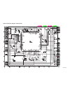
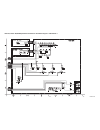
Page 51
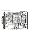
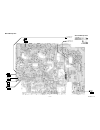
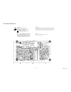
1-12-17 to sensor cba (start-sensor) sw-p vr501 ctl tp513 rf-sw tp302 wf2 c-pb tp301 wf3 v-out tp751 wf1 to sensor cba (end-sensor) s-inh tp502 be9ab0f01011a main cba top view sensor cba top view bhf300f01012a bhf300f01012b.
Page 52
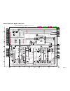
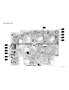
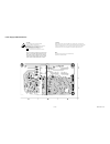
1-12-18 pin21 of tu900 pin 6 of tu900 wf11 wf12 pin 11of tu900 wf13 pin 12 of tu900 wf14 pin 18 of tu900 wf15 pin 2 of ic1406 wf6 pin 14 of cn201 pin 26 of cn201 wf8 pin 28 of cn201 wf7 wf9 pin 22 of cn201 wf5 pin 24 of cn201 wf4 pin 28 of cn2204 wf10 main cba bottom view be9ab0f01011a.
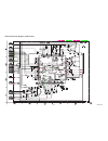
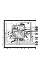
Page 53
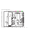
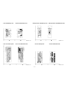
1-12-19 be9a00f01021a power supply cba top view "ce symbole reprèsente un fusible à fusion rapide." caution ! For continued protection against fire hazard, replace only with the same type fuse. Attention : pour une protection continue les risqes d'incele n'utiliser que des fusible de m ê me type. Ri...
Page 54
1-12-20 be9a00f01021a power supply cba bottom view "ce symbole reprèsente un fusible à fusion rapide." caution ! For continued protection against fire hazard, replace only with the same type fuse. Attention : pour une protection continue les risqes d'incele n'utiliser que des fusible de m ê me type....
Page 55
1-12-21 front jack cba top view front jack cba bottom view dvd open/close sw cba top view dvd open/close sw cba bottom view power sw cba top view power sw cba bottom view junction cba top view junction cba bottom view be9a00f01021b be9ab0f01011b be9ab0f01011c be9ab0f01011d.
Page 56: Waveforms
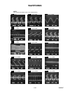
1-13-1 w3nbwf wf9 audio(l)-out pin 14 of cn201 1v 0.5ms wf7 video-cb pin 28 of cn201 0.2v 20 µs wf8 video-cr pin 26 of cn201 0.2v 20 µs spdif 1v 0.1 µs wf10 pin 28 of cn2204 wf4 pin 24 of cn201 video-y 0.2v 20 µs wf5 pin 22 of cn201 video-c 0.2v 20 µs wf6 pin 2 of ic1406 video-cvbs 0.5v 20 µs wf14 p...
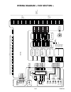
Page 57: Wiring Diagram
Wiring diagram e9ab1wi 1-14-1 ac head assembly audio erase head control head audio head cylinder assembly cn501 cn502 cn504 cn253 cn2209 cn2211 w002 cn2210 full erase head fe head video (r)1 head video (l)1 head video -in2 s-video in2 audio(r) -in2 audio(l) -in2 front video (l)2 head video (r)2 head...
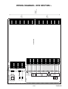
Page 58: Wiring Diagram
Wiring diagram e9ab1wid 1-14-2 to main cba cn2204 (w01) to wiring diagram to main cba cn201 (w02) cn701 video-y(i) 30 gnd 29 video-cr/pr-out 26 gnd 21 video-c-out 22 gnd 27 video-cb/pb-out 28 gnd 25 video-y(i/p)-out 24 gnd 23 cn101 gnd 15 a udio(r)-in 18 gnd 19 a udio(l)-in 20 gnd 17 a udio(r)-out 1...
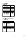
Page 59
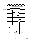
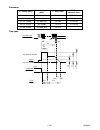
1-15-1 w3n4hti system control timing charts mode sw: ld-sw note: ej rs: loading fwd (lm-fwd / rev “h”) rs ej: loading rev (lm-fwd / rev “l”) stop (a) = loading stop (b) = unloading note: ld-sw position detection a/d input voltage limit (calculated voltage) symbol 3.76 v ~ 4.50 v (4.12 v) ej 4.51 v ~...
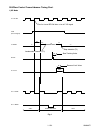
Page 60
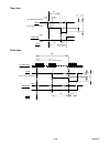
1-15-2 w3n4hti still/slow control frame advance timing chart 1) sp mode fig. 1 23 rf-sw f-ad (internal signal) c-drive pb ctl 32 c-f/r 99 h-a-sw 98 c-rota the first rise of rf-sw after a rise in f-ad signal acceleration detection (t1) at "h" "z" "h" "l" "l" stop detection (t2) st slow tracking value...
Page 61
1-15-3 w3n4hti 2) lp/slp mode fig. 2 23 rf-sw f-ad (internal signal) c-drive pb ctl 32 c-f/r 99 h-a-sw 98 c-rota "h" "z" "h" "l" "l" still still at st bl stop detection (t2) acceleration detection (t1) slow tracking value reversal limit value frame advance the first rise of rf-sw after a rise in f-a...
Page 62
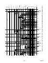
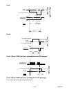
1-15-4 w3n4hti fig. 3 1. Eject (po w er off) -> cassette in (po wer on) -> st op(b) -> st op(a) -> pla y -> rs -> fs -> pla y -> still -> pla y -> st op(a) eject cass.Load st-s/ end-s "off" play rew ff play play stop /eject 0.2s 0.7s 0.4s 0.2s ld-fwd stop(a) stop(a) ld-fwd ld-rev 0.2s ld-fwd ld-fwd ...
Page 63
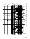
1-15-5 w3n4hti fig. 4 pin no . Ld-sw cl/ss lm-fwd "m" /rev c-drive "z" on on c-f/r dr um r o t a tion p-on-l a-mute-h d-rec-h d-pb ej au rs sf sm tl fb al sb 87 26 32 27 31 29 tv/video 9 displa y st-s/ end-s "on" rec rew ff stop /eject 0.5s 1.0s 0.2s 0.5s 0.2s 0.5s 0.5s 0.5s 0.2s 0.2s 0.2s 1.5s 2.5s...
Page 64
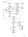
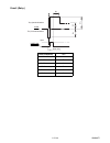
1-15-6 w3n4hti inner-sw open? Rezero 1 to disc distinction power on yes yes no yes tray insertion [ tray open ] button is pressed. [ tray open ] button is pressed. Tray ejection tray ejection completion push close rezero 2 inner-sw open? Is timer et1 passed? Inner-sw open? Is timer et4 passed? Is sl...
Page 65
1-15-7 w3n4hti parameter tray open v*: voltage (hex) s*: encoder pulse (hex) t*: event timer et*: error detection timer v0: 2.0 v (00d) s1: 300 (12c) t1: 0.1 s et1: 5.0 s v1: 4.5 v (022) s2: 3300 (ce4) t2: 3.0 s et2: 5.0 s v2: 2.2 v (010) s3: 3935 (f5f) t3: 3.0 s et3: 3.0 s v3: 2.4 v (013) s4: 0 (00...
Page 66
1-15-8 w3n4hti tray close push close sled inner-sw timer close open tray insertion direction tray ejection direction s5 v3 v4 s4 et3 et4 sled encoder pulse s5 t3 v3 v4 et4 push close inner-sw close open tray insertion direction timer.
Page 67
1-15-9 w3n4hti case 1 case 2 case 3 (when [open] button is pressed before the s5 passage.) case 4 (when [open] button is pressed after the s5 passage.) it starts opening after making closing complete once. Sled open tray insertion direction close inner-sw timer t2 rezero 1 et4 v3 v4 sled inner-sw op...
Page 68
1-15-10 w3n4hti case 5 (retry.) retry frequency v1+ 1st time retry 6 v 2nd time retry 7 v 3rd time retry 8 v 4th time retry 9 v 5th time retry 9 v 6th time retry 9 v sled tray ejection direction s1 v1+ v2 6v open tray insertion direction start retry. Close inner-sw.
Page 69
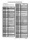
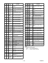
1-16-1 e9ab0pin ic pin function descriptions ic501 (servo/system control/osd) “h” ≥ 4.5 v, “l” ≤ 1.0 v pin no. In/ out signal name function 1 in p-down -h power voltage down detector signal 2 in ready/ busy ready/busy communication control with main micro controller 3 in t-reel take up reel rotation...
Page 70
1-16-2 e9ab0pin notes: abbreviation for active level: pwm ----- pulse wide modulation a/d -------- analog - digital converter 53 out afclpf low pass filter output signal for afc 54 out video- mute video mute control signal 55 out output- select output select (dvd=”l”/ vcr=”h”) 56 out dvd- audio- mut...
Page 71: Lead Identifications
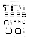
1-17-1 e9ab0le lead identifications 75 26 50 51 25 1 100 76 60 21 40 41 20 1 80 61 e c b e c b 8 1 e c b1 e b2 c1 c2 4 1 1 2 3 4 g d s 16 9 8 1 12 1 32 17 16 1 8 5 4 1 60 21 40 41 20 1 80 61 1 2 4 3 16 9 8 5 24 13 la71205m-mpb-e note: a: anode k: cathode e: emitter c: collector b: base r: reference ...
Page 72
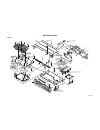
1-18-1 e9ab1cex exploded views cabinet rs501 2b16 dvd mechanism & dvd main cba assembly is supplied as a unit. 2b76 see electrical parts list for parts with this mark. 2l011 2l011 2l011 2l011 2l011 1b1 2l071 2l071 2l071 2l071 2b10 2l043 2l043 2b4 2l043 2l043 2l081 2l081 2l081 2l044 2l044 2l100 2l044...
Page 73
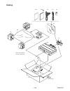
1-18-2 e9ab1pex packing s1 a14 s2 2b64 s2 s2 unit s3 some ref. Numbers are not in sequence. X1 x22 x4 x20 x5 x2 x3 s2.
Page 74: Mechanical Parts List
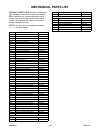
20060914 1-19-1 e9ab1ca mechanical parts list product safety note: products marked with a # have special characteristics important to safety. Before replacing any of these components, read carefully the product safety notice in this service manual. Don't degrade the safety of the product through imp...
Page 75: Electrical Parts List
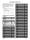
20060914 1-20-1 e9ab1el electrical parts list product safety note: products marked with a # have special characteristics important to safety. Before replacing any of these components, read carefully the product safety notice in this service manual. Don't degrade the safety of the product through imp...
Page 76
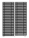
20060914 1-20-2 e9ab1el c462 chip ceramic cap.(1608) b k 0.01 µf/50v chd1jk30b103 c465 electrolytic cap. 4.7 µf/25v m h7 ce1emavsl4r7 c466 electrolytic cap. 220 µf/6.3v m h7 ce0kmavsl221 c467 chip ceramic cap.(1608) b k 0.022 µf/50v chd1jk30b223 c470 chip ceramic cap.(1608) b k 0.1 µf/50v chd1jk30b1...
Page 77
20060914 1-20-3 e9ab1el cn102 ph connector top 2p b2b-ph-k-s (lf)(sn) j3phc02jg029 cn1609 fe connector top 8p 08fe-bt-vk-n jcfej08jg001 diodes d052 zener diode mtzjt-7710b qdtb00mtzj10 d082 pcb jumper d0.6-p10.0 jw10.0t d083 zener diode mtzjt-7718b qdtb00mtzj18 d085 rectifier diode 1n4005 ndqz001n40...
Page 78
20060914 1-20-4 e9ab1el r118 chip res. 1/10w j 47k Ω rrxajr5z0473 r125 carbon res. 1/4w j 220 Ω rcx4jatz0221 r126 chip res. 1/10w j 47k Ω rrxajr5z0473 r127 chip res. 1/10w j 5.6k Ω rrxajr5z0562 r132 carbon res. Rd1/2s101jta rcx2jatz0101 r133 carbon res. 1/4w j 220 Ω rcx4jatz0221 r221 chip res. 1/10w...
Page 79
20060914 1-20-5 e9ab1el r603 chip res. 1/10w j 1.2k Ω rrxajr5z0122 r604 chip res. 1/10w j 1.5k Ω rrxajr5z0152 r605 chip res. 1/10w j 2.2k Ω rrxajr5z0222 r606 chip res. 1/10w j 3.9k Ω rrxajr5z0392 r607 chip res. 1/10w j 8.2k Ω rrxajr5z0822 r608 chip res. 1/10w j 22k Ω rrxajr5z0223 r611 chip res. 1/10...
Page 80
20060914 1-20-6 e9ab1el power sw cba dvd open/close sw cba front jack cba sensor cba psv cba power supply cba jc2 chip res.(1608) 1/10w 0 Ω rrxajr5z0000 jc5 chip res.(1608) 1/10w 0 Ω rrxajr5z0000 jc6 chip res.(1608) 1/10w 0 Ω rrxajr5z0000 jc31 chip res.(1608) 1/10w 0 Ω rrxajr5z0000 jc38 chip res.(16...
Page 81
20060914 1-20-7 e9ab1el junction cba d013 rectifier diode ba158 ndqz000ba158 d014 schottky barrier diode sb190 ndqz000sb190 d015 schottky barrier diode sb340 ndqz000sb340 d016 schottky barrier diode sb340 ndqz000sb340 d017 zener diode mtzjt-7715c qdtc00mtzj15 d018 rectifier diode ba158 ndqz000ba158 ...
Page 82
Cwv20v6 e9ab1cd 2006-10-6.

