Summary of T889
Page 1
M889-00 1 copyright tel 02/10/95 t889 power amplifier uhf fm 800-870mhz issue 100 october 1995 m889-00-100
Page 2
2 m889-00 02/10/95 copyright tel head office new zealand tait electronics ltd 558 wairakei road p.O. Box 1645 christchurch new zealand phone: 64 3 358-3399 fax: 64 3 358-3636 australia tait electronics (aust) pty ltd 275 toombul road northgate 4013 p.O. Box 679 virginia queensland 4014 australia pho...
Page 3: About This Manual
M889-00 3 copyright tel 02/10/95 about this manual scope this manual contains general, technical and servicing informa- tion on the t889 power amplifier. Revision control each page in this manual has a date of issue. This is to comply with various quality standards, but will also serve to identify w...
Page 4: Copyright
4 m889-00 02/10/95 copyright tel copyright all information contained in this manual is the property of tait electronics ltd. All rights are reserved. This manual may not, in whole or part, be copied, photocopied, reproduced, translated stored or reduced to any electronic medium or machine readable f...
Page 5: Table of Contents
M889-00 5 copyright tel 02/10/95 table of contents this manual is divided into seven sections as listed below. There is a detailed table of contents at the start of each section. Section title 1 general information 2 circuit operation 3 introduction to servicing 4 initial tuning & adjustment 5 fault...
Page 6: List Of Effective Pages
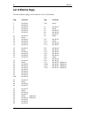
6 m889-00 02/10/95 copyright tel list of effective pages the total number of pages in this manual is 64, as listed below. Page issue date page issue date 1 02/10/95 2 02/10/95 3 02/10/95 4 02/10/95 5 02/10/95 6 02/10/95 1.1 02/10/95 1.2 blank 1.3 02/10/95 1.4 02/10/95 1.5 02/10/95 1.6 02/10/95 2.1 0...
Page 7: General Information
M889-00 general information 1.1 copyright tel 02/10/95 1 general information this section provides a brief description of the t889 pa, along with detailed specifica- tions and a list of variants available. The following topics are covered in this section. Section title page 1.1 introduction 1.3 1.2 ...
Page 8
1.2 general information m889-00 02/10/95 copyright tel.
Page 9: 1.1
M889-00 general information 1.3 copyright tel 02/10/95 1.1 introduction the t889 is an fm base station power amplifier designed for single or multichannel operation within the frequency range 800 to 870mhz. The output power capability is 20 to 100w. The pa comprises a broad band, two stage drive amp...
Page 10: 1.2
1.4 general information m889-00 02/10/95 copyright tel 1.2 specifications 1.2.1 introduction the performance figures given are minimum figures, unless otherwise indicated, for equipment tuned with the maximum switching band and operating at standard room temperature (+22 ° c to +28 ° c). Where appli...
Page 11
M889-00 general information 1.5 copyright tel 02/10/95 spurious emissions: conducted - transmit .. -36dbm to 1ghz -30dbm to 4ghz - standby .. -57dbm to 1ghz -47dbm to 4ghz radiated - transmit .. -36dbm to 1ghz -30dbm to 4ghz - standby .. -57dbm to 1ghz -47dbm to 4ghz dimensions: height .. 191mm widt...
Page 12: 1.3
1.6 general information m889-00 02/10/95 copyright tel 1.3 versions description version 10 800-870mhz.
Page 13: Circuit Operation
M889-00 circuit operation 2.1 copyright tel 02/10/95 2 circuit operation this section provides a basic description of the circuit operation of the t889 pa. The following topics are covered in this section. Section title page 2.1 introduction 2.3 2.2 rf circuitry 2.3 2.3 2.3.1 2.3.2 2.3.3 2.3.4 2.3.5...
Page 14
2.2 circuit operation m889-00 02/10/95 copyright tel.
Page 15: 2.1
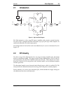
M889-00 circuit operation 2.3 copyright tel 02/10/95 2.1 introduction figure 2.1 high level block diagram the t889 comprises a three stage rf power amplifier with extensive control circuitry. The final stage is composed of four transistors (q3, q4, q5 & q6) whose outputs are combined to provide the ...
Page 16: 2.3
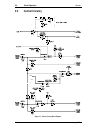
2.4 circuit operation m889-00 02/10/95 copyright tel 2.3 control circuitry figure 2.2 control circuitry block diagram ref.
Page 17
M889-00 circuit operation 2.5 copyright tel 02/10/95 2.3.1 power control the dc voltages from the directional coupler representing forward and reflected power are buffered by the two voltage followers, ic3 pins 1, 2 & 3 and pins 5, 6 & 7. Their out- puts are summed at an integrator (ic1 pins 8, 9 & ...
Page 18
2.6 circuit operation m889-00 02/10/95 copyright tel 2.3.5 forward and reverse power metering forward and reverse power signals from the two ic3 buffers are available for metering purposes. The output currents are adjustable via rv43 (forward power) and rv57 (reverse power). 2.3.6 fan control circui...
Page 19: Introduction To Servicing
M889-00 introduction to servicing 3.1 copyright tel 02/10/95 3 introduction to servicing this section provides some general and advisory information on servicing procedures. The following topics are covered in this section. Section title page 3.1 3.1.1 3.1.2 3.1.3 general caution: cmos devices cauti...
Page 20
3.2 introduction to servicing m889-00 02/10/95 copyright tel.
Page 21: 3.1
M889-00 introduction to servicing 3.3 copyright tel 02/10/95 3.1 general if you require further information about the t889 or this manual, contact your nearest authorised tait dealer or service centre. Further assistance may be obtained from the customer support group, radio infrastructure division,...
Page 22
3.4 introduction to servicing m889-00 02/10/95 copyright tel 3.1.3 caution: beryllium oxide & power transistors the rf power transistors in current use all contain some beryllium oxide. This sub- stance, while perfectly harmless in its normal solid form, can become a severe health hazard when it has...
Page 23: 3.2
M889-00 introduction to servicing 3.5 copyright tel 02/10/95 3.2 mechanical 3.2.1 pozidriv recess head screws pozidriv recess head screws are the preferred standard on all tait manufactured equip- ment. The very real advantages of this type of screw will not be realised unless the cor- rect screwdri...
Page 24: 3.3
3.6 introduction to servicing m889-00 02/10/95 copyright tel 3.3 component replacement 3.3.1 leaded components whenever components are removed from or fitted to the pcb, care must be taken to avoid damage to the track. The two satisfactory methods of removing components from pth pcbs are detailed be...
Page 25
M889-00 introduction to servicing 3.7 copyright tel 02/10/95 3.3.2 surface mount devices caution: surface mount devices (smd's) require special storage, handling, removal and replacement techniques. This equipment should be serv- iced only by an approved tait dealer or service centre equipped with t...
Page 26: 3.4
3.8 introduction to servicing m889-00 02/10/95 copyright tel 3.4 to replace pa transistors caution: as the location of certain components in the pa is critical to perform- ance, it is important that any components removed or disturbed are refitted in exactly the same position. Caution: do not solder...
Page 27
M889-00 introduction to servicing 3.9 copyright tel 02/10/95 figure 3.2 typical transistor/capacitor spacing (q1 & q2 shown) grounding clips b b b b b c c b measurement a q1 q2.
Page 28: 3.5
3.10 introduction to servicing m889-00 02/10/95 copyright tel 3.5 to remove the pcb from the heatsink most components are soldered topside only, but in some cases access to the underside of the pcb is necessary. Remove the d-range connector. Disconnect the power feed to the fan. Remove the 13 pcb re...
Page 29: Initial Tuning & Adjustment
M889-00 initial tuning & adjustment 4.1 copyright tel 02/10/95 4 initial tuning & adjustment the following section describes the initial set-up procedures, including alarm adjust- ment and power meter calibration. The following topics are covered in this section. Section title page 4.1 initial conne...
Page 30
4.2 initial tuning & adjustment m889-00 02/10/95 copyright tel.
Page 31: 4.1
M889-00 initial tuning & adjustment 4.3 copyright tel 02/10/95 4.1 initial connections connect the pa to a power supply, an output rf load and a power meter as detailed below: power supply rating >30a rf load >150w. Provide a keyed rf drive at the required frequency. Connect the drive source key lin...
Page 32: 4.5
4.4 initial tuning & adjustment m889-00 02/10/95 copyright tel 4.5 high reverse power alarm set rv63 to the required output power. Connect a known mismatch of the required value to the pa output. Apply rf drive and tx key. Adjust rv52 (reverse power alarm) so that the front panel high reverse power ...
Page 33: Fault Finding
M889-00 fault finding 5.1 copyright tel 02/10/95 5 fault finding the following test procedures and fault finding flow charts may be used to help locate a hardware problem, however they are by no means a complete fault finding procedure. If the fault still exists after having progressed through them ...
Page 34
5.2 fault finding m889-00 02/10/95 copyright tel.
Page 35: 5.1
M889-00 fault finding 5.3 copyright tel 02/10/95 5.1 visual checks remove the cover from the t889 and inspect the pcb for damaged or broken com- ponents, paying particular attention to the surface mounted devices (smd's). Check for defective solder joints. If repair or replacement is considered nece...
Page 36: 5.4
5.4 fault finding m889-00 02/10/95 copyright tel 5.4 rf checks the pa fault finding chart (section 5.5.1) provides a systematic approach for locating a fault in the rf circuitry. Use this chart in conjunction with figure 5.1, which shows the locations of the 50 Ω input and output test points for rf ...
Page 37
M889-00 fault finding 5.5 copyright tel 02/10/95 replace a4 pages 5.5/5.6 with a3 pages 5.5/5.6, file name 88900_5a.100
Page 38
5.6 fault finding m889-00 02/10/95 copyright tel replace a4 pages 5.5/5.6 with a3 pages 5.5/5.6, file name 88900_5a.100
Page 39: 5.5
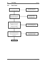
M889-00 fault finding 5.7 copyright tel 02/10/95 5.5 fault finding charts 5.5.1 pa is maximum power >90w @ 800-870mhz? Are rv69 & rv63 fully clockwise? Is the drive from the exciter 4w? Rotate clockwise: rv63 first, rv69 second. Set drive to 4w. Rf circuitry ok. Replace splitter hybrid. Check collec...
Page 40
5.8 fault finding m889-00 02/10/95 copyright tel 5.5.2 power control use rv63 to adjust output power to 60w. Adjust rv48 until forward power led is just lit. Power control ok. N n n y y y y ensure rv69 is fully clockwise. Check sense voltages from directional coupler on ic3 pins 1 & 7. With the 3db ...
Page 41
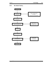
M889-00 fault finding 5.9 copyright tel 02/10/95 5.5.3 fan control circuitry key transmitter. Does fan run at room temperature? Spray "freeze" on r116 or short r113. Does the low temperature inhibit circuit stop the fan? Spray "freeze" on r116 or short r113. Check ic3 pin 14 >11v. Check q21 & q20. N...
Page 42
5.10 fault finding m889-00 02/10/95 copyright tel.
Page 43
M889-00 fault finding 5.5 copyright tel 02/10/95.
Page 44
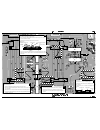
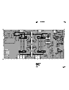
5.6 fault finding m889-00 02/10/95 copyright tel t889 pcb layout bottom side l46 c97 c98 l19 l29 l96 c59 l22 l16 l32 l26 l1 l49 l43 l12 l39 l33 c45 c38 c15 c32 c25 output test lead - q1 & q2 1. Desolder c15 and resolder on edge as shown. 2. Remove the wireline clamping plate and solder the test lead...
Page 45: Installation
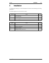
M889-00 installation 6.1 copyright tel 02/10/95 6 installation the following section gives a brief description of the basic rack mounting and wiring procedures. The following topics are covered in this section. Section title page 6.1 rack mounting 6.3 6.2 rack wiring 6.5 6.3 power supply 6.5 figure ...
Page 46
6.2 installation m889-00 02/10/95 copyright tel.
Page 47: 6.1
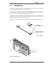
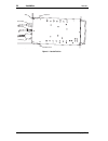
M889-00 installation 6.3 copyright tel 02/10/95 6.1 rack mounting the t889 pa is designed for use in a standard 483mm rack frame using the supporting guide rails supplied with the unit (refer to figure 6.1). The lower guide rail is located in the rack frame with three screws, two at the rear and one...
Page 48
6.4 installation m889-00 02/10/95 copyright tel figure 6.3 latched position stop rf output top rail rf input d-range bottom rail.
Page 49: 6.2
M889-00 installation 6.5 copyright tel 02/10/95 6.2 rack wiring wire the d-range connector as shown in figure 6.4. Ensure that the cables are not sub- jected to any stresses due to tight bends or incorrect lengths. The rf coaxial cables to the bnc and n-type connectors should be free from acute bend...
Page 50
6.6 installation m889-00 02/10/95 copyright tel.
Page 51: Pcb Information
M889-00 pcb information 7.1.1 copyright tel 02/10/95 7 pcb information this section provides parts lists, a grid reference index, pcb layouts and circuit diagrams for the t889 pa. This section contains the following information. Section title ipn page 7.1 introduction 7.1.3 7.2 t889 pa pcb 220-01326...
Page 52
7.1.2 pcb information m889-00 02/10/95 copyright tel.
Page 53: 7.1
M889-00 pcb information 7.1.3 copyright tel 02/10/95 7.1 introduction pcb identification all pcbs are identified by a unique 10 digit number, the last 2 digits of which define the issue status. The issue status starts at 00 and increments through 01, 02, 03, etc. As the pcb is updated. Some issue pc...
Page 54
7.1.4 pcb information m889-00 02/10/95 copyright tel the line to indicate where the rest of the circuitry is located. The first digit refers to the sheet number (printed on the bottom right hand corner of the cad diagram) and the last two characters refer to the location on that sheet of the continu...
Page 55: 7.2
M889-00 pcb information 7.2.1 copyright tel 02/10/95 7.2 t889 pa pcb this section contains the following information. Ipn section page 220-01326-01 parts list mechanical & miscellaneous parts grid reference index pcb layout - bottom side pcb layout - top side rf section circuit diagram control secti...
Page 56
7.2.2 pcb information m889-00 02/10/95 copyright tel t889 parts list (ipn 220-01326-01) how to use this parts list the components listed in this parts list are divided into two main types: those with a circuit reference (e.G. C2, d1, r121, etc) and those without (miscellaneous and mechanical). Those...
Page 57
M889-00 pcb information 7.2.3 copyright tel 02/10/95 ref var ipn description ref var ipn description d3 001-00011-60 (s) diode sr2607 6a/30v d4 001-10000-70 (s) diode smd bav70 dual switch sot-23 co d6 001-10000-70 (s) diode smd bav70 dual switch sot-23 co d13 001-10000-70 (s) diode smd bav70 dual s...
Page 58
7.2.4 pcb information m889-00 02/10/95 copyright tel ref var ipn description ref var ipn description r113 036-15270-00 res m/f 0805 chip 27k 5% r115 036-16470-00 res m/f 0805 chip 470k 5% r116 045-04470-01 res ntc 4k7 5% 5mm disc r117 036-15150-00 res m/f 0805 chip 15k 5% r118 036-14390-00 res m/f 0...
Page 59
M889-00 pcb information 7.2.5 copyright tel 02/10/95 ipn description ipn description t889 mechanical & miscellaneous parts (220-01326-01) 012-04150-01 cap cer f/thru 1n5 no lead c1-c15 051-00006-02 solder spring 1.3mm a4m1877 (x6) (led wire joints) 065-00010-13 bead ferrite 7d 1.9*0.9*3.8mm stack po...
Page 60
7.2.6 pcb information m889-00 02/10/95 copyright tel.
Page 61
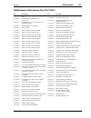
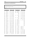
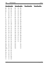
M889-00 pcb information 7.2.7 copyright tel 02/10/95 t889 grid reference index (ipn 220-01326-01) how to use this grid reference index the first digit in the pcb layout reference is a "1" or "2", indicating the top or bottom side layout respectively, and the last two charac- ters give the location o...
Page 62
7.2.8 pcb information m889-00 02/10/95 copyright tel device pcb circuit device pcb circuit device pcb circuit device pcb circuit q17 1:u5 2-r7 q18 1:u5 2-s8 q19 1:w7 2-p8 q20 1:w8 2-q7 q21 1:w3 2-q5 q22 1:w5 2-m0 q23 1:t7 2-p0 q24 1:t8 2-q0 q25 1:u7 2-p2 r1 1:q5 1-c3 r2 1:s6 1-d4 r3 1:s5 1-c4 r4 1:q...
Page 63
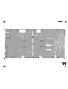
M889-00 pcb information 7.2.9 copyright tel 02/10/95 t889 pcb layout bottom side 220-01326-01.
Page 64
7.2.10 pcb information m889-00 02/10/95 copyright tel t889 pcb layout top side 220-01326-01 l46 c97 c98 l19 l29 l96 c59 l22 l16 l32 l26 l1 l49 l43 l12 l39 l33 c45 c38 c15 c32 c25.
Page 65
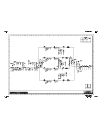
M889-00 pcb information 7.2.11 copyright tel 02/10/95 t889 rf section 220-01326-01.
Page 66
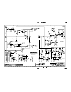
7.2.12 pcb information m889-00 02/10/95 copyright tel t889 control section - 220-01326-01.


