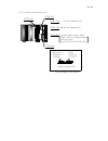
1 / 13 (ver.0.1) model: tl-5150s takenaka sensor group takenaka system co.,ltd. □ h e a d o f f i c e 86-66 nomizo-cho otsuka yamashina-ku 607-8135 kyoto japan tel:+81-75-593-9300 fax +81-75-593-9790 □ i n s p e c t i o n s y s t e m d e p t . 86-66 nomizo-cho otsuka yamashina-ku 607-8135 kyoto japa...
2 / 13 table of contents 1. Outline ………………………………………………… 4 2. Features ………………………………………………… 4 3.Applications ………………………………….…………… 4 4.Specifications …………………………………………… 4 5. Camera i/o ……………………………………………… 5 5-1. Power source 5-2. I/o connector 6. Timing chart ……………………………………………… 7 7. Exposure control ……………...
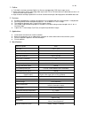
3 / 13 ● note that the contents of this manual are subject to change without notice for improvement. ● all contents of this manual are subject to the copyright owned by takenaka system company. Unauthorized copy inhibited. The brief history of takenaka system co. Takenaka system co.( trade mark:take...
4 / 13 1. Outline ● tl-5150s is the high-resolution digital line scanner equipped with ccd linear image sensor. ● digital video signal (10 bit) and analog video signal (0 to 2.5v at 75 Ω-terminated) are delivered at a time as in the case of ufd series camera. ● high-resolution and high-speed ccd lin...
5 / 13 5. Camera i / o 5-1 power source power is supplied through 15 pin connector. Though ripple-free and stable power source is preferable, the switching supply is also employable. In general, ripple voltage of a stabilized power source is approx.35mv, and approx.120mv for a switching supply. As v...
6 / 13 ● power connector [dsub 15pins male] ● digital out connector [hirose: dx20a36s] ● sync connector……connector for monitoring internal sync signal it can be monitored by oscilloscope. Signal level is ttl level. Pin no. Signal name pin no. Signal name 1 shield 9 nc 2 +12v 10 gnd 3 gnd 11 nc 4 nc ...
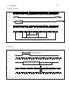
7 / 13 6. Timing chart e xt sy nc in e xt cl k in s yn c o ut pulse width of sync:100nsec or more (ext clk 20mhz or more) d ata d ata c lo ck ou t 56 clk removal period 5nsec data setup time 12.5nsec±3nsec s 1 100 clk s 2 s 3 s 4 e xt cl k in c lk du ty r ati o m in 40 %, ma x 6 0% d ata c lo ck ou ...
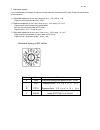
8 / 13 7. Exposure control it can switch between three types of exposure control modes by manipulating exp switch (exposure control switch) on the rear panel. ① line period exposure (at scan rate 7.54khz or less) exp setting n=0 exposure during each period of ext sync ② fixed time exposure (at scan ...
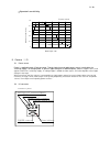
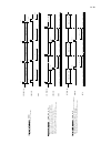
9 / 13 st o ut - 1 e x t. Sy n c i n s y nc o u t f i x e d t i m e e x po s u re (s w = n、 n = 1 t o e ) e x p o s u r e d u r i n g t h e p e r i od o f t h e e q u a t i o n b e l o w f r o m t h e t i m i n g o f l e a d in g e d g e o f e x t . S y n c ( c c 1 ) . E x p o s u r e t i m e = d a ...
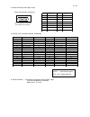
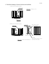
10 / 13 8. Illustrative drawing of internal structure and switches (a) side view of internal structure pcb2-cn6 pcb2-cn6 pcb1-vr1 (b) side view of internal structure pcb2-sw1 gain selector switch pcb2-sw1 on off 1 to 3 in sw1 1 2 3 off off off on off off off on off on on off off off on on off on off...
11 / 13 (c) top view of internal structure pcb3-vr2 pcb3-vr1 pcb3-vr2 wc level adjusting vr pcb3-vr1 black level adjusting vr pcb4-sw2 external input selector switch 15pin connector/36pinconnector selector switch for ext sync and clk input pcb4-sw2 digital out power connector connector (36 pins) (15...
12 / 13 9. Notes precautions for use ■ do not make an impact on the equipment. ■ do not lag the equipment with heat insulating agent. If the equipment is covered with heat insulating agent, it produces an increase in temperature and it causes the equipment to malfunction.(except for low-temperature ...
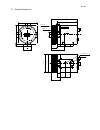
13 / 13 10. External dimensions e l e m e nt s ync vi deo ex p d ig it al o ut po wer ( f our fa ces ) 6 6 8 . 2 6 3 . 5 8 6 3. 5 2 7 . 6 φ 6 3 φ 6 3 . 8 1 1 . 2 1 7 . 5 1 7 . 5 3 0 . 5 k- m o u n t m 2. 6 de pt h6 2 - m 6 d e p th 8 1 / 4- 2 0 u n c d e p th 8 f b : 4 5 . 5 (19.3) 1 8 8 7 . 5.

