- DL manuals
- Themis
- Motherboard
- USPIIi-1v
- Hardware Manual
Themis USPIIi-1v Hardware Manual
Summary of USPIIi-1v
Page 1
Uspiii-1v hardware manual revision b4.
Page 3
Themis computer—rest of world 20 rue du tour de l’eau 38400 saint martin d’hères, france phone +33 476 59 60 46 fax +33 476 59 60 49 themis computer—americas and pacific rim 3185 laurelview court fremont, ca 94538 phone (510) 252-0870 fax (510) 490-5529 world wide web http://www.Themis.Com uspiii-1v...
Page 4
Copyright © 2000 themis computer, inc. All rights reserved. No part of this publication may be reproduced in any form, by photocopy, microfilm, retrieval system, or by any other means now known or hereafter invented without the prior written permission of themis computer. The information in this pub...
Page 5
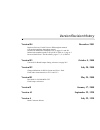
Version revision history version b4 december 2001 replaced universe ii with universe iib throughout manual. Corrected misspellings throughout manual. Reenforced definition of backplane reset on pages 2-2 and b-2. Defined non-standard signal for p2 pin b3 in table a-2, page a-3. Reversed serial port ...
Page 6
Uspiii-1v user’s manual themis computer.
Page 7
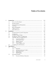
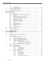
Themis computer v table of contents 1 introduction ........................................................................................................... 1-1 1.1 how to use this manual ....................................................................................... 1-1 1.2 intended audie...
Page 8
Uspiii-1v hardware manual vi themis computer 3.2.2 i/o subsystem........................................................................................ 3-5 3.2.3 auxiliary functions ............................................................................... 3-6 3.3 environmental specification.....
Page 9
Themis computer vii table of contents 5.5 universe iib’s interrupt and interrupt handler ..................................................... 5-14 5.5.1 vme and pci interrupters:.................................................................... 5-14 5.5.2 vmebus interrupt handling: .................
Page 10
Uspiii-1v hardware manual viii themis computer a.2.10 push-button reset .............................................................................. A-13 a.3 i/o board ............................................................................................................... A-14 a.3.1 i/o boa...
Page 11
Themis computer ix list of tables table 2-1. Summary of different connectors configuration.................................................................... 2-4 table 3-1. Processor specifications.........................................................................................................
Page 12
Uspiii-1v hardware manual x themis computer table 6-4. Watchdog por enable/disable ............................................................................................ 6-2 table 6-5. Watchdog enable/disable ........................................................................................
Page 13
Themis computer xi list of figures figure 3-1. Uspiii-1v baseboard block diagram.................................................................................. 3-3 figure 4-1. Memory sub-system topology ........................................................................................... 4-...
Page 14
Uspiii-1v hardware manual xii themis computer figure b-2. I/o board jumper locations ...............................................................................................B-5 figure b-3. Baseboard component side solder bead locations ............................................................
Page 15
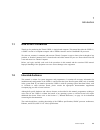
Themis computer 1-1 1 1 introduction 1.1 how to use this manual thank you for purchasing the themis uspiii-1v single board computer. This manual describes the uspiii-1v, a sparc version 9.0 compliant computer with a vmebus interface and an ultrasparc-iii processor. We value our customer’s comments a...
Page 16
Uspiii-1v hardware manual 1-2 themis computer 1.3 product warranty and registration please review the themis computer warranty and complete the product registration card delivered with your uspiii-1v board(s). Return of the registration card is not required to activate your product warranty but, by ...
Page 17
Themis computer 1-3 1. Introduction • a micro db9 connector to male, db25 console adapter cable for the baseboard console (tty a) port; themis part number 108113. • a 68 pin, sub-miniature connector to 0.005”, male standard scsi-3 connector adapter cable for the baseboard scsi a; themis part number ...
Page 18
Uspiii-1v hardware manual 1-4 themis computer 1.6 chapter overview this document is organized in chapters and appendices of increasing information content and detail. A brief outline of the contents of each chapter is provided: • chapter 1, "introduction," contains a brief overview of this document,...
Page 19
Themis computer 1-5 1. Introduction • ieee standard p1275.6/d4, standard for boot (initialization, configuration) firmware, 64 bit extensions • openboot 3.X command reference, sun microsystems (802-5837-10, rev a) • pci bus binding to ieee 1275-1994, standard for boot (initialization, configuration)...
Page 20
Uspiii-1v hardware manual 1-6 themis computer.
Page 21
Themis computer 2-1 2 2 installation 2.1 determine board type and configuration check the white sticker located on your board’s p2 connector. It contains information on board type, serial number and release number. Example: [ uspiii-1v/1-2mb-512-440 a1] [s1300786] – board type: uspiii-1v/1 – extende...
Page 22
Uspiii-1v hardware manual 2-2 themis computer 2.2 configuration when you first receive the uspiii-1v, confirm that the installation of jumpers is appropriate to your application . Refer to appendix § b jumper and solder bead configurations for a complete listing of jumper definitions. The default ju...
Page 23
Themis computer 2-3 2. Installation • pin b6 should be jumpered to pin b7 (bg1) • pin b8 should be jumpered to pin b9 (bg2) • pin b10 should be jumpered to pin b11 (bg3) 2.4 installing the uspiii-1v paddle board the paddle board, also referred to as a “transition board”, attaches to the rear of the ...
Page 24
Uspiii-1v hardware manual 2-4 themis computer 2.5 attaching cables to peripheral devices attach adapter cables to the appropriate front panel and p2 paddle board connectors. The following sections provide information on what adapter cables are required and how to attach them. Also refer to appendice...
Page 25
Themis computer 2-5 2. Installation 2.5.2 keyboard and mouse in ps/2 mode: attach one end of cable 108114 to the front panel “ “kybd/mouse” connector and the two other ends to a ps/2 keyboard and a ps/2 mouse. In sun mode: attach one end of cable 108783 to the front panel “console” connector and the...
Page 26
Uspiii-1v hardware manual 2-6 themis computer either at the front or at the back), onboard scsi terminators will be activated to terminate that end of the scsi bus. When the board is sitting in the middle of the scsi chain (i.E. Devices connected both at the front and at the back), onboard terminato...
Page 27
Themis computer 3-1 3 3 specification 3.1 overview the uspiii-1v is available under four product configurations: • uspiii-1v/1, “uspiii-1v baseboard” is the single slot baseboard. • uspiii-1v/2c, “uspiii-1v with graphics and expanded i/o” provides the uspiii-1v baseboard and, in the second slot, an ...
Page 28
Uspiii-1v hardware manual 3-2 themis computer the local i/o subsystem is pci based, with separate pci channels provided for i/o functions and external vmebus backplane access. Scsi ports a and b, ethernet a, console port and ps/2 keyboard/mouse connections are provided on the front panel of the base...
Page 29
Themis computer 3-3 3. Specification 3.1.5 block diagram figure 3-1. Uspiii-1v baseboard block diagram ultrasparc-iii e-cache dram interface pci interface memory mezzanine 72 xcvers buffers e do dram chips edo dr am chips addr/ 144 pci-vme 66mhz 32-bit pci scsi ethernet a super i/o tod flash e-bus s...
Page 30
Uspiii-1v hardware manual 3-4 themis computer 3.2 system specification 3.2.1 processor & memory subsystems below are the processor and memory subsection specifications. Table 3-1. Processor specifications feature/function specifications processor ultrasparc-iii processor speed grade 1 - 360 mhz grad...
Page 31
Themis computer 3-5 3. Specification 3.2.2 i/o subsystem table 3-3, "i/o sub-system specification," on page 3-5, summarizes the i/o subsystem functionality of the various product configurations. Table 3-3. I/o sub-system specification function single slot (baseboard) dual slot (baseboard, creator gr...
Page 32
Uspiii-1v hardware manual 3-6 themis computer * key: fp - interface via front panel connector p2 - interface via p2 connector slot 1, 2, and 3 refer to the position of the vme slots. Baseboard is always on slot 1. 3.2.3 auxiliary functions table 3-4, "auxiliary functions specifications," on page 3-6...
Page 33
Themis computer 3-7 3. Specification 3.3 environmental specification when measuring the operating environment air temperature for the uspiii-1v, measure the air temperature as close to the air intake port on the enclosure as possible. Although the thermal characteristics of the uspiii-1v are quite g...
Page 34
Uspiii-1v hardware manual 3-8 themis computer 3.4 estimated power requirements table 3-7. Estimated power requirements configuration (uspiii-1v/1 with 360/440 mhz processor) watts dissipation (typical) 128 mbytes memory 32/34 watts 256 mbytes memory 34/36 watts 1024 mbytes memory 35/37 watts.
Page 35
Themis computer 4-1 4 4 hardware overview 4.1 major components the following sections provide a description of the major of the uspiii-1v. More detailed explanations of certain subsystems is provided in later sections and chapters. 4.1.1 sme ultrasparc-iii processor and cache the central processor f...
Page 36
Uspiii-1v hardware manual 4-2 themis computer • the i-mmu is disabled • the ultrasparc-iii is in red_state • the access is mapped by the i-mmu as physically non-cacheable data accesses to non-cacheable pci or upa64s space occur when either: • the d-mmu enable bit (dm) in the lsu_control_register is ...
Page 37
Themis computer 4-3 4. Hardware overview 4.1.6 sme pci i/o controller the sme pci i/o controller (sme: stp2003qfp) is a +5 volt asic that provides a master / slave interface bus compliant with pci local bus specification, revision 2.1. The pci i/o is connected to the sme apb via the local pci bus. M...
Page 38
Uspiii-1v hardware manual 4-4 themis computer the 8 mb user flash is made of two 4mx8 bit sharp lh28f320. User flash contains the openboot prom (obp) specially configured for the sun mode. Either the system flash or the user flash may be used for board boot-up, selectable by jumper setting. Make sur...
Page 39
Themis computer 4-5 4. Hardware overview 10-bit column addressing is supported on the modules. Considerable attention was paid to minimize the power consumption of uspiii-1v. The maximum active power consumption of a 64 mb memory module is 4.212 watts. . Figure 4-1. Memory sub-system topology 4.3 pm...
Page 40
Uspiii-1v hardware manual 4-6 themis computer • reads non-volatile ram (nvram) and executes the boot sequence. The diagnostic executive or standalone programs can also be executed. • includes the abbreviated system monitor. Entry into the system monitor is signified by the “ok” prompt. If a boot att...
Page 41
Themis computer 5-1 5 5 universe-iib description 5.1 features tundra’s universe iib (ca91c142) interfaces the local 32-bit pci bus to the vmebus. The following lists some of the universe iib’s features on the uspiii-1v board: • 33 mhz, 32-bit pci bus interface • fully compliant, high performance 64-...
Page 42
Uspiii-1v hardware manual 5-2 themis computer 5.2 uspiii-1v and the universe iib pci interface the following table lists some of the pci signals of the uspiii-1v to the universe iib’s pci interface. 5.3 vmebus interface 5.3.1 vmebus configuration the following lists the initial configuration of the ...
Page 43
Themis computer 5-3 5. Universe-iib description cycle operation is selected, the transaction is completed on the pci bus first, and the data acknowledgment is sent to the vmebus master. With the coupled cycle, the vmebus is not available to other masters while the pci bus is executing the transactio...
Page 44
Uspiii-1v hardware manual 5-4 themis computer figure 5-1. Universe iib architectural diagram the universe iib’s vmebus master interface supports all of the addressing and data transfer modes as specified by the vme64 specification. The universe iib does not support the a64 mode and modes intended to...
Page 45
Themis computer 5-5 5. Universe-iib description when the universe iib is configured as the system controller, it provides the following functions on the vmebus: – a 16mhz clock driver – an arbitration module – a bus timer – an iack daisy chain driver (dcd). The uspiii-1v supports round-robin arbitra...
Page 46
Uspiii-1v hardware manual 5-6 themis computer refer to “auto slot id: vme64 specified”, on page 2-24, and “auto-id: a proprietary tundra method”, on page 2-25 of the universe iib manual for more information. 5.3.4.2 registered access at the power up register access at the power up is used in a syste...
Page 47
Themis computer 5-7 5. Universe-iib description the pci configuration base address 0 and base address 1 registers offsets are 0x010 and 0x014, respectively. The registers specify the 4kb aligned base address of the 4 kb universe iib register space on pci. The power-up options determine if the regist...
Page 48
Uspiii-1v hardware manual 5-8 themis computer 5.4.1 vme slave images a vmebus slave image is used to access the resources of the pci bus when the universe ii is not the vmebus master. The user may control the type of accesses by programming specific attributes of the vmebus slave image. The universe...
Page 49
Themis computer 5-9 5. Universe-iib description figure 5-2. Address translation for vmebus to pci bus transfers 5.4.1.3 control fields a vmebus slave image is enabled using the en bit of the control field. The control field also specifies how reads and writes are processed: either as a coupled trans...
Page 50
Uspiii-1v hardware manual 5-10 themis computer 5.4.2.1 pci bus fields decoding for vmebus accesses is based on the address and command information produced by a pci bus master. The pci target interface claims a cycle if there is an address match and if the command matches certain criteria. The pci t...
Page 51
Themis computer 5-11 5. Universe-iib description 5.4.2.3 control fields through the control fields, the user specify how writes are processes and enable a pci target image. The pci target image is enabled by setting the en bit. Posted writes are performed when the pwen bit is set and the particular ...
Page 52
Uspiii-1v hardware manual 5-12 themis computer the 64 mb space is divided into four (4), 16 mb spaces that are selected using ad[25:16]. For each region, the upper 64 kb map to vmebus a16 space, while the remaining portion map to vmebus a24 space. The addressing of this slave image is depicted in fi...
Page 53
Themis computer 5-13 5. Universe-iib description 15:12 pgm [3..0] r/w 0 program/data am code each of the four bits specifies program/data am code for the cor- responding 16 mb region. The lower order bits correspond to the lower order address regions. 0 = data, 1 = program 11:8 super [3..0] r/w 0 su...
Page 54
Uspiii-1v hardware manual 5-14 themis computer figure 5-4. Memory mapping in the special pci target image 5.5 universe iib’s interrupt and interrupt handler 5.5.1 vme and pci interrupters: for the vmebus, the interrupt source can be mapped to any of the vmebus interrupt output pins such as virq#[7.....
Page 55
Themis computer 5-15 5. Universe-iib description interrupts mapped to the pci bus interrupt output pin (int0#) are serviced by the pci interrupt controller. The ultrasparc-iii determines which interrupt sources are active by reading the interrupt status register in the universe iib. The interrupt is...
Page 56
Uspiii-1v hardware manual 5-16 themis computer 5.5.6 dma controller the universe iib utilizes an internal dma controller for high performance data transfer between the vmebus and the pci bus. Universe iib’s parameters for the dma transfer are software configurable. Dma operations between the source ...
Page 57
Themis computer 6-1 6 6 fpga, watchdog, voltage and temperature sensors 6.1 fpga 6.1.1 introduction the fpga device on the uspiii-1v is the altera epf882 and resides on the ebus2 of the baseboard pci i/o asics. Physically, the fpga is located on the baseboard. The fpga implements a voltage monitor, ...
Page 58
Uspiii-1v hardware manual 6-2 themis computer the boot address decoder selects between boot access of the system flash, the rombo connector, or user flash 1. Selection is made by jumpers j3303 and j3304. The tables below show the address maps related to the pcio’s internal address space for all jump...
Page 59
Themis computer 6-3 6. Fpga, watchdog, voltage and temperature sensors when no watchdogs have expired the uspiii-1v is in a ‘normal’ state. When the level 1 watchdog expires, a maskable interrupt is sent to the ric. The uspiii-1v is considered to be in a ‘warning’ state. Upon expiration, the level 2...
Page 60
Uspiii-1v hardware manual 6-4 themis computer power management system entering coping state will turn the front alarm led to amber. In failed state, the led will turn red and the power fail signal will be asserted on vme p2. See appendix a.2.2, "baseboard vme p2," and appendix a.2.9, "leds." the pow...
Page 61
Themis computer 6-5 6. Fpga, watchdog, voltage and temperature sensors 6.2 temperature sensor the temperature sensor is implemented using registers in the fpga and the dallas semiconductor ds1620 digital thermometer and thermostat. The dallas ds1620 provides 9-bit temperature readings which indicate...
Page 62
Uspiii-1v hardware manual 6-6 themis computer.
Page 63
Themis computer 7-1 7 7 resets 7.1 overview this chapter presents a brief discussion of the reset structure of the uspiii-1v. The various types of resets, some possible reset sources, and reset effects are explained. Resets are used to force all or part of the system into a known state. A reset is d...
Page 64
Uspiii-1v hardware manual 7-2 themis computer the system, or part of the system, may also be reset by a watchdog reset (wdr) or a software-initiated reset (sir). These resets originate within the ultrasparc-iii core and are only observed by the processor core. Depending on the conditions and type of...
Page 65
Themis computer 7-3 7. Resets note that a wdr reset initiated internal to the processor is different that the 3-level watchdog implemented in the fpga of the uspiii-1v. For further explanation of the 3-level watchdog section 7.3.4, "3-level watchdog resets," on page 7-4. 7.2.4 software initiated res...
Page 66
Uspiii-1v hardware manual 7-4 themis computer 7.3.3 vmebus resets a system reset from the vmebus is received by the universe iib asic through the vme p1 connector. The universe iib asserts local_reset to the epld. The epld will de-assert power_ok to the ric when it receives local_reset and initiate ...
Page 67
Themis computer 7-5 7. Resets 7.4 ultrasparc-iii reset control register the ultrasparc-iii reset_control register indicate the source of a reset and provides control of software reset generation. It is located at 0x1fe.0000.F020. Table 7-1. Ultrasparc-iii reset_control register field bits value desc...
Page 68
Uspiii-1v hardware manual 7-6 themis computer 7.5 uspiii-1v reset tree diagram. Figure 7-1. Uspiii-1v reset diagram 1 1. Internal to the ultrasparc-iii are the watch dog reset (wdr) and software initiated reset (sir). These two resets are initiated within the processor core and effect only the proce...
Page 69
Themis computer a-1 a a connector pinouts, leds, switches a.1 introduction the following appendix provides the connector pinouts for the user interfaces on the uspiii-1v as well as descriptions of other user interfaces such as leds and switches. The baseboard, i/o board, pmc carrier board, and paddl...
Page 70
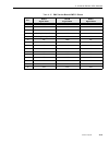
Uspiii-1v hardware manual a-2 themis computer table a-1. Baseboard vme p1 pinout pin row a signal name row b signal name row c signal name 1 vme d00 vme bbsy vme d08 2 vme d01 vme bclr vme d09 3 vme d02 vme acfail vme d10 4 vme d03 vme bgin0 vme d11 5 vme d04 vme bgout0 vme d12 6 vme d05 vme bgin1 v...
Page 71
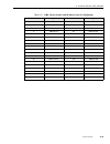
Themis computer a-3 a. Connector pinouts, leds, switches a.2.2 baseboard vme p2 scsi port a, ethernet mii port a and alarm signals are routed to p2. Additional p2 pinout varies with the board configuration: in ps/2 mode, either ps/2 keyboard/mouse signals or serial port b signals are available on p2...
Page 72
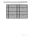
Uspiii-1v hardware manual a-4 themis computer 13 mii a tx en vcc scsi a dat 14 mii a txd0 vme d16 scsi a dat 15 mii a txd1 vme d17 scsi a dat 16 mii a txd2 vme d18 scsi a dat 17 mii a txd3 vme d19 scsi a dat 18 mii a col vme d20 scsi a dat 19 mii a crs vme d21 scsi a dat 20 serial b txd or do not co...
Page 73
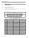
Themis computer a-5 a. Connector pinouts, leds, switches table a-3. Baseboard vme p2 connector in sun mode pin row a signal name row b signal name row c signal name 1 vcc vcc vcc 2 mii a mdio gnd scsi a p2 a 3 mii a mdc scsi a termpwr scsi a termpwr 4 mii a rxd3 vme a24 scsi a atn 5 mii a rxd2 vme a...
Page 74
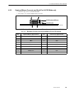
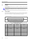
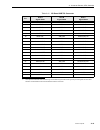
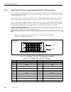
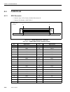
Uspiii-1v hardware manual a-6 themis computer a.2.3 scsi a and b • connector type: honda dual scsi-3 (40 mb/sec) connector, 68 pin, 0.8 mm pitch • connector part number: hdra-e68wildt-sl figure a-3. Baseboard scsi a and b connector orientation table a-4. Baseboard scsi a and b pinout pin signal name...
Page 75
Themis computer a-7 a. Connector pinouts, leds, switches 21 gnd 55 atn 22 gnd 56 gnd 23 gnd 57 bsy 24 gnd 58 ack 25 gnd 59 rst 26 gnd 60 msg 27 gnd 61 sel 28 gnd 62 cd 29 gnd 63 req 30 gnd 64 io 31 gnd 65 dat 32 gnd 66 dat 33 gnd 67 dat 34 gnd 68 dat a. This is part of the automatic scsi termination...
Page 76
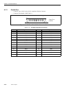
Uspiii-1v hardware manual a-8 themis computer a.2.4 rj45 ethernet a connector • connector type: rj-45 tpe figure a-4. Ethernet a connector orientation table a-5. Rj45 ethernet a pinout pin signal name 1 txd+ 2 txd- 3 rxd+ 4 4t_d3p 5 4t_d3p 6 rxd- 7 4t_d4p 8 4t_d4p 8 1 front view of pcb.
Page 77
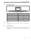
Themis computer a-9 a. Connector pinouts, leds, switches a.2.5 keyboard/mouse connector and serial port a (ps/2 mode only) • connector type: two (2), stacked mini-db9 • part number: itt cannon mdsm-18pe-z10-vr25 figure a-5. Baseboard console and keyboard/mouse connector orientation (ps/2 mode) table...
Page 78
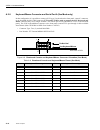
Uspiii-1v hardware manual a-10 themis computer a.2.6 ps/2 keyboard/mouse split cable figure a-6. Ps/2 keyboard/mouse split cable table a-7. Ps/2 keyboard/mouse split cable pinout front panel keyboard/ mouse connector pin number signal name ps/2 keyboard pin number a a. Pins 2 and 6 of the keyboard c...
Page 79
Themis computer a-11 a. Connector pinouts, leds, switches a.2.7 serial port a (console) adapter cable (ps/2 mode only) figure a-7. Serial port adapter cable table a-8. Serial port a (console) adapter cable front panel serial port a (console) pinout signal name serial port a cable pinout a a. All unl...
Page 80
Uspiii-1v hardware manual a-12 themis computer a.2.8 keyboard/mouse connector and serial port a (sun mode only) in that configuration, it is possible to connect a sun type 5 keyboard on the front panel “console” connector, or on the paddle board #1 db9 connector. Ttya and ttyb are used to support th...
Page 81
Themis computer a-13 a. Connector pinouts, leds, switches a.2.9 leds an “alarm” and a “ready” led are located on the front panel of the baseboard. • the “alarm” led has three possible colors: green, amber or red. Refer to chapter 6, "fpga, watchdog, voltage and temperature sensors," for detailed inf...
Page 82
Uspiii-1v hardware manual a-14 themis computer a.3 i/o board for a diagram of the i/o board front panel refer to appendix c.3, "baseboard, i/o board, and creator graphics front panels." caution — as vme p1 is not populated, the position occupied by the i/o board (position #2 on uspiii-1v/ 2c and 1v/...
Page 83
Themis computer a-15 a. Connector pinouts, leds, switches 13 mii b tx en vcc scsi b dat 14 mii b txd0 vme d16 scsi b dat 15 mii b txd1 vme d17 scsi b dat 16 mii b txd2 vme d18 scsi b dat 17 mii b txd3 vme d19 scsi b dat 18 mii b col vme d20 scsi b dat 19 mii b crs vme d21 scsi b dat 20 serial c/d tx...
Page 84
Uspiii-1v hardware manual a-16 themis computer a.3.2 serial port c (ttyc or console) and serial port d (ttyd or aux port) in sun mode, the two baseboard serial ports (ports a and b) are used by the keyboard and mouse logic, respectively. Therefore, serial port c becomes the software console port (al...
Page 85
Themis computer a-17 a. Connector pinouts, leds, switches 11 txc+ 37 txc+ 12 nc 38 nc 13 cts+ 39 cts+ 14 txd+ 40 txd+ 15 nc 41 nc 16 rxd+ 42 rxd+ 17 rxc- 43 rxc- 18 nc 44 nc 19 rts+ 45 rts+ 20 dtr- 46 dtr- 21 nc 47 nc 22 nc 48 nc 23 dtr+ 49 dtr+ 24 txc- 50 txc- 25 nc 51 nc 26 nc 52 nc table a-12. I/...
Page 86
Uspiii-1v hardware manual a-18 themis computer a.3.3 parallel port • connector type: 0.050, 26 pin, sub d, amplimite slimline connector • connector part number: amp 750823-1 figure a-11. I/o board parallel port connector orientation table a-13. I/o board parallel port pinout pins signal name pins si...
Page 87
Themis computer a-19 a. Connector pinouts, leds, switches a.3.4 rj45 ethernet b connector • connector type: rj-45 tpe figure a-12. Ethernet b connector orientation a.3.5 audio a standard miniature audio jack is used for audio line-in and audio line-out. The part used is the aston at-jy3540-050b. A.3...
Page 88
Uspiii-1v hardware manual a-20 themis computer a.4 pmc carrier board for a diagram of the pmc board front panel refer to . A.4.1 pmc carrier board p1 connector the p1 connector provides daisy-chaining of iack and bg signals. There is no need to jumper those signals manually for the position occupied...
Page 89
Themis computer a-21 a. Connector pinouts, leds, switches 18 nc nc nc 19 gnd nc nc 20 nc gnd nc 21 daisy_chain_iack# nc nc 22 daisy_chain_iack# nc nc 23 nc gnd nc 24 nc nc nc 25 nc nc nc 26 nc nc nc 27 nc nc nc 28 nc nc nc 29 nc nc nc 30 nc nc nc 31 -12v nc +12v 32 vcc vcc vcc table a-15. Pmc carrie...
Page 90
Uspiii-1v hardware manual a-22 themis computer a.4.2 pmc carrier board vme p2 connector the vme p2 connector of the pmc carrier can contain either 64 user-defined signals from pmc slot #1, or 32 signals from pmc slot #1 and 32 from pmc slot #2. • connector type: vme32 figure a-14. Pmc board vme p2 c...
Page 91
Themis computer a-23 a. Connector pinouts, leds, switches 22 pmc io a22 gnd pmc io c22 23 pmc io a23 nc pmc io c23 24 pmc io a24 nc pmc io c24 25 pmc io a25 nc pmc io c25 26 pmc io a26 nc pmc io c26 27 pmc io a27 nc pmc io c27 28 pmc io a28 nc pmc io c28 29 pmc io a29 nc pmc io c29 30 pmc io a30 nc ...
Page 92
Uspiii-1v hardware manual a-24 themis computer a.4.3 pmc carrier slot user i/o this section provides the pinout of the 64 pmc user i/o signals that can be brought from pmc cards to the vme p2 connector of the pmc carrier board. Also see appendix a.4.2, "pmc carrier board vme p2 connector," for addit...
Page 93
Themis computer a-25 a. Connector pinouts, leds, switches 14 pmc io a7 46 pmc io a23 15 pmc io c8 47 pmc io c24 16 pmc io a8 48 pmc io a24 17 pmc io c9 49 pmc io c25 18 pmc io a9 50 pmc io a25 19 pmc io c10 51 pmc io c26 20 pmc io a10 52 pmc io a26 21 pmc io c11 53 pmc io c27 22 pmc io a11 54 pmc io...
Page 94
Uspiii-1v hardware manual a-26 themis computer a.4.3.2 pmc carrier slot #1: 32 bit user i/o configuration table a-18. Pmc carrier slot #1 with 32 bits of user i/o pin number signal pin number signal 1 nc 33 pmc io c17 2 nc 34 pmc io a17 3 nc 35 pmc io c18 4 nc 36 pmc io a18 5 nc 37 pmc io c19 6 nc 3...
Page 95
Themis computer a-27 a. Connector pinouts, leds, switches a.4.3.3 pmc carrier slot #2: 32 bit user i/o configuration table a-19. Pmc carrier slot #2 with 32 bits of user i/o pin number signal pin number signal 1 pmc io c1 33 nc 2 pmc io a1 34 nc 3 pmc io c2 35 nc 4 pmc io a2 36 nc 5 pmc io c3 37 nc ...
Page 96
Uspiii-1v hardware manual a-28 themis computer a.5 paddle board a.5.1 scsi connector • connector type: 68 pin, female, shielded subminature-d • connector part number: amp 787082-7 figure a-16. Paddle board scsi connector table a-20. Paddle board scsi connector pinout pin signal name pin signal name ...
Page 97
Themis computer a-29 a. Connector pinouts, leds, switches 20 scsi p2 a 54 gnd 21 gnd 55 atn 22 gnd 56 gnd 23 gnd 57 bsy 24 gnd 58 ack 25 gnd 59 reset 26 gnd 60 msg 27 gnd 61 sel 28 gnd 62 cd 29 gnd 63 req 30 gnd 64 io 31 gnd 65 dat8 32 gnd 66 dat9 33 gnd 67 dat10 34 gnd 68 dat11 a. This is part of t...
Page 98
Uspiii-1v hardware manual a-30 themis computer a.5.2 mii connector • connector type: 40 pin, female, subminiature-d • connector part number: amp 787170-4 figure a-17. Paddle board mii connector table a-21. Paddle board mii connector pinout pin signal name pin signal name 1 vcc 21 vcc 2 mii_mdio 22 g...
Page 99
Themis computer a-31 a. Connector pinouts, leds, switches a.5.3 db9 connector the exact signals available on the paddle board db9 connector vary with the board configuration, as described in table 2-1, "summary of different connectors configuration.," on page 2-4. • connector type: male, right angel...
Page 100
Uspiii-1v hardware manual a-32 themis computer.
Page 101
Themis computer b-1 b b jumper and solder bead configurations b.1 overview this appendix provides a summary of the solder beads and jumpers configuration on the uspiii-1v. Jumpers are considered to be ‘field configurable’ and may be altered by a user on site. Solder beads are considered to be factor...
Page 102
Uspiii-1v hardware manual b-2 themis computer caution — jumper jp3303, boot from system flash, and jumper jp3304, boot from user flash should not both be set to 1-2. If this does occur system flash will take precedence over user flash. In order to boot from the user flash, set jp3303 to 2-3 and jp33...
Page 103
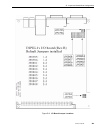
Themis computer b-3 b. Jumper and solder bead configurations figure b-1. Baseboard jumper locations jp3302 jp3303 jp4902 jp3301 jp1401 jp1601 jp3801 j1501 jp3304 1 2 7 8 jp4901 jp1502 jp3901 jp4201 uspiii-1v - default jumpers installed jp1401 1-2 jp1601 2-3 jp3801 1-2 jp3901 1-2 all other jumpers ar...
Page 104
Uspiii-1v hardware manual b-4 themis computer b.2.2 i/o board jumpers note — for each serial port, all jumpers selecting between rs232 and rs422 operation must be set correctly. Figure b-2 "i/o board jumper locations" on page b-5, provides the location of the various jumpers on the uspiii-1v baseboa...
Page 105
Themis computer b-5 b. Jumper and solder bead configurations figure b-2. I/o board jumper locations.
Page 106
Uspiii-1v hardware manual b-6 themis computer b.2.3 pmc carrier board jumpers there are no jumpers on the pmc carrier board. B.3 factory configurables b.3.1 baseboard solder beads table b-3. Baseboard component side solder beads solder bead setting description sb3202 open (default) chassis gnd rf is...
Page 107
Themis computer b-7 b. Jumper and solder bead configurations figure b-3 "baseboard component side solder bead locations" on page b-8 and figure b-4 "baseboard solder side solder bead locations" on page b-9 provide the location of the baseboard solder beads. Sb3304 1-2 +5 v to flash (default) 2-3 +12...
Page 108
Uspiii-1v hardware manual b-8 themis computer figure b-3. Baseboard component side solder bead locations sb3302 sb2401 sb3202.
Page 109
Themis computer b-9 b. Jumper and solder bead configurations figure b-4. Baseboard solder side solder bead locations sb3305 sb3304 sb1401 sb3303 sb3203 1 1 1 3 3 3 sb3301 sb3501 sb3502 3 1 3 1 3 1 3 1 3 1 3 1 3 1 3 1 sb1808 sb1801 3 1 3 1 sb1809 3 1 sb1811.
Page 110
Uspiii-1v hardware manual b-10 themis computer b.3.2 i/o board solder beads the location of the i/o board solder side solder beads is provided in figure b-5 "i/o board solder side solder beads" on page b-10. Figure b-5. I/o board solder side solder beads b.3.3 pmc carrier board solder beads there ar...
Page 111
Themis computer c-1 c c front panel diagrams c.1 introduction the following sections present diagrams of the front panels for all possible configurations of the uspiii-1v. It is intended as a quick reference for the front panel user i/o on the product..
Page 112
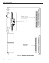
Uspiii-1v hardware manual c-2 themis computer c.2 baseboard front panel figure c-1. Single slot front panel console (ttya) ps/2 keyboard / mouse scsi port a scsi port b power_ok_led system_ok_led push button reset ej ec t o r rj 45 alarm ready reset uspiii-1v/1: single slot c o n f igura tion ej ec ...
Page 113
Themis computer c-3 c. Front panel diagrams c.3 baseboard, i/o board, and creator graphics front panels figure c-2. Double slot front panels console (ttya) ps/2 keyboard / mouse scsi port a scsi port b power_ok_led system_ok_led push button reset ej ec t o r rj 45 alarm ready reset uspiii-1v/2p: tri...
Page 114
Uspiii-1v hardware manual c-4 themis computer c.4 baseboard, i/o board, and pmc carrier board front panel figure c-3. Triple slot front panel pm c sl o t # 2 pm c slot #1 pm c slot #3 sun kb/ms or console ps/2 keyboard / mouse scsi port a scsi port b power_ok_led system_ok_led push button reset ej e...
Page 115
Themis computer d-1 d d board diagrams d.1 baseboard board diagrams.
Page 116
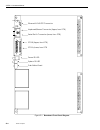
Uspiii-1v hardware manual d-2 themis computer figure d-1. Baseboard front panel diagram ethernet a rj45-tpe connector keyboard/mouse connector (upper, from pcb) serial port a connector (lower, from pcb) scsi b (upper, from pcb) scsi a (lower, from pcb power ok led system ok led push-button reset.
Page 117
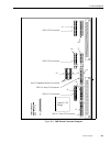
Themis computer d-3 d. Board diagrams figure d-2. Baseboard component diagram power trends pt6503a: 2.5v dc-dc voltage convertor power trends pt6501a: 3.3v dc-dc voltage convertor sme 1040 ultrasparc-ii i sme2411: advance pci bridge sme stp2210: reset, interrupt, and clock national super i/o pc87307...
Page 118
Uspiii-1v hardware manual d-4 themis computer figure d-3. Baseboard connector diagram memory card connectors expanded i/o connector creator graphics, pmc carrier board upa connector.
Page 119
Themis computer d-5 d. Board diagrams d.2 i/o board diagrams figure d-4. I/o board component side line-in line-out ethernet b tty c (upper connector) tty d (lower connector) parallel siemens 82532: uart sme stp2003: cheerio vme p2 connector pm c c ar rier c o nn ect or crystal cs4231akq: codec d c.
Page 120
Uspiii-1v hardware manual d-6 themis computer d.3 pmc board figure d-5. Pmc carrier board component side j9 j10 j6 j7 j8 j11 j12 j3 j4 j5 digital 21150 bridge user i/o adapter connectors pm c c ar rie r# 3 pm c c ar rie r# 2 pmc c a rri e r# 1.
Page 121
Themis computer d-7 d. Board diagrams figure d-6. Pmc board connector diagram j9 j10 j6 j7 j8 j11 j12 j3 j4 j5 digital 21150 bridge user i/o adapter board connectors pmc #1 user i/o connector pmc #1 connectors pmc #2 connectors pmc #3 connectors pmc #2 user i/o connector.
Page 122
Uspiii-1v hardware manual d-8 themis computer d.4 paddle board figure d-7. Paddle board component side vme p2 serial port b (db-9) amp 787170-4 mii ethernet (miniature db40) amp: 787082-7 scsi a (miniature db68) amp: 757844-2.
Page 123
Themis computer e-1 e e glossary e.1 terminology the terminology used in this manual generally follows industry conventions. The following list defines the specific meanings of words and terms as used in this section. A16: addressing on address line a[15..1], as specified in ansi vme64 specification...
Page 124
Uspiii-1v hardware manual e-2 themis computer hardware: on the uspiii-1v, cpu module, cables, peripheral devices are typical examples of hardware. May: a keyword indicating flexibility of choice with no implied preference. Led: light-emitting diode mii: medium independent interface mmu: memory manag...
Page 125
Themis computer e-3 . Tsb: translation storage buffer. A one-level, software data structure that maintains address translation information. Separate tsbs reside both in the mmu and the iom. Virtual address: an address produced by a processor that maps all system-wide, program-visible memory. Virtual...
Page 126
Uspiii-1v hardware manual e-4 themis computer.
Page 127
Themis computer 3185 laurelview court fremont, ca 94538 attn: publications department place stamp here.
Page 128
Reader comment card we welcome your comments and suggestions to help improve the uspiii-1v user’s manual. Please take time to let us know what you think about these manuals. • the information provided in the manuals was complete. Agree___ disagree___ not applicable___ • the information was well docu...


