- DL manuals
- Xilinx
- Transceiver
- 7 Series
- User Manual
Xilinx 7 Series User Manual - Reset and Initialization
38
7 Series FPGAs GTP Transceivers User Guide
UG482 (v1.9) December 19, 2016
Chapter 2:
Shared Features
Reset and Initialization
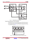
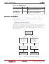
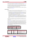
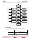
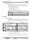
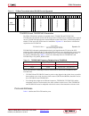
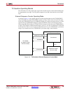
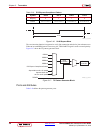
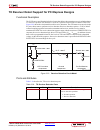
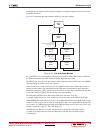
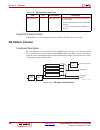
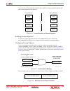
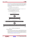
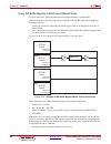
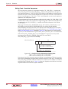
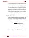
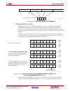
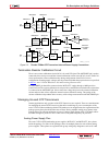
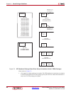
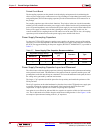
The GTP transceiver must be initialized after FPGA device power-up and configuration before it
can be used. The GTP transceiver’s transmitter (TX) and receiver (RX) can be initialized
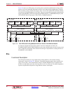
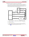
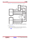
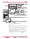
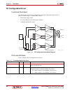
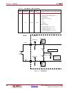
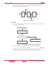
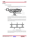
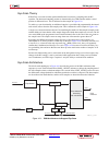
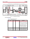
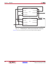
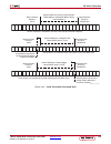
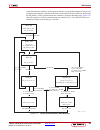
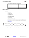
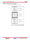
independently and in parallel as shown in
. The GTP transceiver’s TX and RX
initialization comprises two steps:
1. Initializing the associated PLL driving TX/RX
2. Initializing the TX and RX datapaths (PMA + PCS)
The GTP transceiver’s TX and RX can receive a clock from either PLL0 or PLL1. The associated
PLL (PLL0 /PLL1) used by the TX and RX must be initialized first before TX and RX initialization.
Any PLL used by the TX and RX is reset individually and its reset operation is completely
independent from all TX and RX resets. The TX and RX datapaths must be initialized only after the
associated PLL is locked.
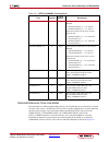
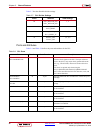
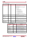
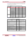
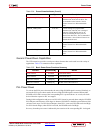
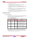
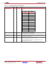
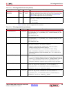
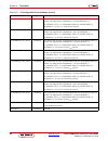
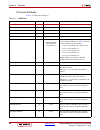
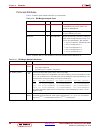
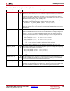
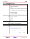
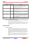
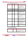
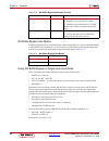
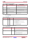
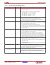
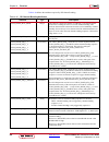
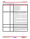
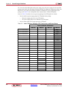
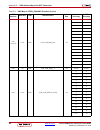
PLL0_INIT_CFG
PLL1_INIT_CFG
24-bit Hex
Reserved. The recommended value from the 7 Series
FPGAs Transceivers Wizard should be used.
PLL0_DMON_CFG
PLL1_DMON_CFG
1-bit Binary
Reserved. The recommended value from the 7 Series
FPGAs Transceivers Wizard should be used.
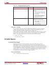
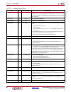
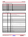
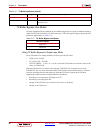
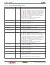
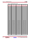
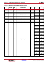
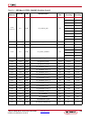
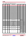
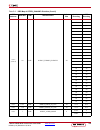
Table 2-9: PLL Attributes (Cont’d)
Attribute
Type
Description
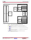
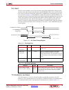
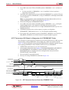
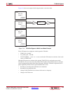
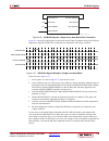
X-Ref Target - Figure 2-11
Figure 2-11: GTP Transceiver Initialization Overview
After FPGA
Configuration
Initialize PLL
(PLL0/PLL1)
used by TX
TX Initialization By
GTTXRESET
TXRESETDONE
RXRESETDONE
RX Initialization By
GTRXRESET
Initialize PLL
(PLL0/PLL1)
used by RX
UG482_c2_15_040412
Summary of 7 Series
Page 1
7 series fpgas gtp transceivers user guide ug482 (v1.9) december 19, 2016.
Page 2: Revision History
7 series fpgas gtp transceivers user guide www.Xilinx.Com ug482 (v1.9) december 19, 2016 disclaimer the information disclosed to you hereunder (the “materials”) is provided solely for the selection and use of xilinx products. To the maximum extent permitted by applicable law: (1) materials are made ...
Page 3
Ug482 (v1.9) december 19, 2016 www.Xilinx.Com 7 series fpgas gtp transceivers user guide 10/23/2012 1.3 added artix-7 device in functional description, page 25 , single external reference clock use model, page 32 , and multiple external reference clock use model, page 33 . Deleted xc7a350t in figure...
Page 4
7 series fpgas gtp transceivers user guide www.Xilinx.Com ug482 (v1.9) december 19, 2016 04/03/2014 1.7 added devices xc7a35t-cpg236, xc7a50t-cpg236, and xc7z015-clg485. Changed sim_version type from “real” to “string” in table 1-3 . Changed rx rate change from “rx pcs” to “entire rx” in table 2-22 ...
Page 5: Table of Contents
7 series fpgas gtp transceivers user guide www.Xilinx.Com 5 ug482 (v1.9) december 19, 2016 revision history . . . . . . . . . . . . . . . . . . . . . . . . . . . . . . . . . . . . . . . . . . . . . . . . . . . . . . . . . . . . . . 2 preface: about this guide guide contents . . . . . . . . . . . . ....
Page 6
6 www.Xilinx.Com 7 series fpgas gtp transceivers user guide ug482 (v1.9) december 19, 2016 chapter 4: receiver rx overview . . . . . . . . . . . . . . . . . . . . . . . . . . . . . . . . . . . . . . . . . . . . . . . . . . . . . . . . . . . . . . . 125 rx analog front end . . . . . . . . . . . . . ....
Page 7
7 series fpgas gtp transceivers user guide www.Xilinx.Com 7 ug482 (v1.9) december 19, 2016 appendix b: placement information by device appendix c: 8b/10b valid characters appendix d: drp address map of the gtp transceiver send feedback.
Page 8
8 www.Xilinx.Com 7 series fpgas gtp transceivers user guide ug482 (v1.9) december 19, 2016 send feedback.
Page 9: About This Guide
7 series fpgas gtp transceivers user guide www.Xilinx.Com 9 ug482 (v1.9) december 19, 2016 preface about this guide xilinx® 7 series fpgas include four fpga families that are all designed for lowest power to enable a common design to scale across families for optimal power, performance, and cost. Th...
Page 10: Additional Resources
10 www.Xilinx.Com 7 series fpgas gtp transceivers user guide ug482 (v1.9) december 19, 2016 preface: about this guide additional resources to find additional documentation, see the xilinx website at: http://www.Xilinx.Com/support/documentation/index.Htm . To search the answer database of silicon, so...
Page 11: Overview and Features
7 series fpgas gtp transceivers user guide www.Xilinx.Com 11 ug482 (v1.9) december 19, 2016 chapter 1 transceiver and tool overview overview and features the 7 series fpgas gtp transceiver is a power-efficient transceiver, supporting line rates between 500 mb/s and 6.6 gb/s. The gtp transceiver is h...
Page 12
12 www.Xilinx.Com 7 series fpgas gtp transceivers user guide ug482 (v1.9) december 19, 2016 chapter 1: transceiver and tool overview the gtp transceiver offers a data rate range and features that allow physical layer support for various protocols including: • pci express, revision 1.1/2.0 • interlak...
Page 13
7 series fpgas gtp transceivers user guide www.Xilinx.Com 13 ug482 (v1.9) december 19, 2016 overview and features additional information on the functional blocks of 7 series fpgas is available at: ug470 , 7 series fpgas configuration user guide provides more information on the configuration. Ug471 ,...
Page 14
14 www.Xilinx.Com 7 series fpgas gtp transceivers user guide ug482 (v1.9) december 19, 2016 chapter 1: transceiver and tool overview four gtpe2 channels clustered together with one gtpe2_common primitive are called a quad or q. The gtpe2_common primitive contains two ring oscillator plls (pll0 and p...
Page 15
7 series fpgas gtp transceivers user guide www.Xilinx.Com 15 ug482 (v1.9) december 19, 2016 overview and features figure 1-3 illustrates the topology of a gtpe2_channel primitive. Refer to figure 2-9, page 35 for the description of the channel clocking architecture, which provides clocks to the rx a...
Page 16: Simulation
16 www.Xilinx.Com 7 series fpgas gtp transceivers user guide ug482 (v1.9) december 19, 2016 chapter 1: transceiver and tool overview 7 series fpgas transceivers wizard the 7 series fpgas transceivers wizard (hereinafter called the wizard) is the preferred tool to generate a wrapper to instantiate gt...
Page 17
7 series fpgas gtp transceivers user guide www.Xilinx.Com 17 ug482 (v1.9) december 19, 2016 simulation secureip models are encrypted versions of the verilog hdl used for implementation of the modeled block. Secureip is an ip encryption methodology. To support secureip models, a verilog lrm - ieee st...
Page 18
18 www.Xilinx.Com 7 series fpgas gtp transceivers user guide ug482 (v1.9) december 19, 2016 chapter 1: transceiver and tool overview ports and attributes there are no simulation-only ports on the gtpe2_common and gtpe2_channel primitives. Gtpe2_common attributes the gtpe2_common primitive has attrib...
Page 19
7 series fpgas gtp transceivers user guide www.Xilinx.Com 19 ug482 (v1.9) december 19, 2016 simulation gtpe2_channel attributes the gtpe2_channel primitive has attributes intended only for simulation. Table 1-3 lists the simulation-only attributes of the gtpe2_channel primitive. The names of these a...
Page 20: Implementation
20 www.Xilinx.Com 7 series fpgas gtp transceivers user guide ug482 (v1.9) december 19, 2016 chapter 1: transceiver and tool overview implementation functional description this section provides the information needed to map 7 series gtp transceivers instantiated in a design to device resources, inclu...
Page 21
7 series fpgas gtp transceivers user guide www.Xilinx.Com 21 ug482 (v1.9) december 19, 2016 implementation serial transceiver channels by device/package see ug475 , 7 series fpgas packaging and pinout specification. X-ref target - figure 1-5 figure 1-5: four channel configuration ug482_c1_05_110811 ...
Page 22
22 www.Xilinx.Com 7 series fpgas gtp transceivers user guide ug482 (v1.9) december 19, 2016 chapter 1: transceiver and tool overview send feedback.
Page 23: Shared Features
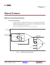
7 series fpgas gtp transceivers user guide www.Xilinx.Com 23 ug482 (v1.9) december 19, 2016 chapter 2 shared features reference clock input structure functional description the reference clock input structure is illustrated in figure 2-1 . The input is terminated internally with 50 Ω on each leg to ...
Page 24
24 www.Xilinx.Com 7 series fpgas gtp transceivers user guide ug482 (v1.9) december 19, 2016 chapter 2: shared features ports and attributes table 2-1 defines the reference clock input ports in the ibufds_gte2 software primitive. Table 2-2 defines the attributes in the ibufds_gte2 software primitive ...
Page 25
7 series fpgas gtp transceivers user guide www.Xilinx.Com 25 ug482 (v1.9) december 19, 2016 reference clock selection and distribution use modes: reference clock termination the reference clock input is to be externally ac coupled. Table 2-3 shows the port and attribute settings required to achieve ...
Page 26
26 www.Xilinx.Com 7 series fpgas gtp transceivers user guide ug482 (v1.9) december 19, 2016 chapter 2: shared features figure 2-3 shows the shows the detailed view of the reference clock multiplexer structures within a single gtpe2_common primitive. The pll0refclksel and pll1refclksel ports are requ...
Page 27
7 series fpgas gtp transceivers user guide www.Xilinx.Com 27 ug482 (v1.9) december 19, 2016 reference clock selection and distribution ports and attributes table 2-4 and table 2-5 define the clocking ports and attributes for the gtpe2_common primitive. X-ref target - figure 2-3 figure 2-3: pll0 and ...
Page 28
28 www.Xilinx.Com 7 series fpgas gtp transceivers user guide ug482 (v1.9) december 19, 2016 chapter 2: shared features gtwestrefclk1 in clock west-bound clock from the quad on the right side of the device. Gteastrefclk0 in clock east-bound clock from the quad on the left side of the device. Gteastre...
Page 29
7 series fpgas gtp transceivers user guide www.Xilinx.Com 29 ug482 (v1.9) december 19, 2016 reference clock selection and distribution pll0refclksel[2:0] in async input to dynamically select the input reference clock to pll0. This input should be set to 3'b001 when only one clock source is connected...
Page 30
30 www.Xilinx.Com 7 series fpgas gtp transceivers user guide ug482 (v1.9) december 19, 2016 chapter 2: shared features table 2-6 defines the clocking ports for the gtpe2_channel primitive. Table 2-5: gtpe2_common attributes attribute type description sim_pll0refclk_sel 3-bit binary this attribute se...
Page 31
7 series fpgas gtp transceivers user guide www.Xilinx.Com 31 ug482 (v1.9) december 19, 2016 reference clock selection and distribution external reference clock use model each quad has two dedicated differential reference clock inputs that can be connected to external reference clock sources. An ibuf...
Page 32
32 www.Xilinx.Com 7 series fpgas gtp transceivers user guide ug482 (v1.9) december 19, 2016 chapter 2: shared features single external reference clock use model in the single external reference clock use model, the user connects the ibufds_gte2 output (o) to the gtrefclk0 input port of the gtpe2_com...
Page 33
7 series fpgas gtp transceivers user guide www.Xilinx.Com 33 ug482 (v1.9) december 19, 2016 reference clock selection and distribution figure 2-6 shows a single reference clock connected to two gtp quads. The user connects the ibufds_gte2 output (o) to the gtrefclk0 input port of both gtpe2_common p...
Page 34: Pll
34 www.Xilinx.Com 7 series fpgas gtp transceivers user guide ug482 (v1.9) december 19, 2016 chapter 2: shared features figure 2-8 shows two gtp quads, each utilizing their own dedicated differential reference clock inputs as well as the dedicated differential reference clock inputs of their neighbor...
Page 35
7 series fpgas gtp transceivers user guide www.Xilinx.Com 35 ug482 (v1.9) december 19, 2016 pll the pll input clock selection is described in reference clock selection and distribution, page 25 . The pll outputs feed the tx and rx clock divider blocks, which control the generation of serial and para...
Page 36
36 www.Xilinx.Com 7 series fpgas gtp transceivers user guide ug482 (v1.9) december 19, 2016 chapter 2: shared features table 2-7 lists the allowable divider settings. Ports and attributes table 2-8 and table 2-9 defines the ports and attributes for the pll. Table 2-7: pll divider settings factor att...
Page 37
7 series fpgas gtp transceivers user guide www.Xilinx.Com 37 ug482 (v1.9) december 19, 2016 pll pll0refclksel[2:0] pll1refclksel[2:0] in async input to dynamically select the input reference clock to the pll. This input should be set to 3'b001 when only one clock source is connected to the pll refer...
Page 38: Reset and Initialization
38 www.Xilinx.Com 7 series fpgas gtp transceivers user guide ug482 (v1.9) december 19, 2016 chapter 2: shared features reset and initialization the gtp transceiver must be initialized after fpga device power-up and configuration before it can be used. The gtp transceiver’s transmitter (tx) and recei...
Page 39
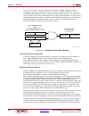
7 series fpgas gtp transceivers user guide www.Xilinx.Com 39 ug482 (v1.9) december 19, 2016 reset and initialization the gtp transceiver’s tx and rx use a state machine to control the initialization process. They are partitioned into a few reset regions. The partition allows the reset state machine ...
Page 40
40 www.Xilinx.Com 7 series fpgas gtp transceivers user guide ug482 (v1.9) december 19, 2016 chapter 2: shared features for major coverage differences between initialization and component resets, refer to table 2-16 for the gtp transceiver’s tx and table 2-20 and table 2-21 for the gtp transceiver’s ...
Page 41
7 series fpgas gtp transceivers user guide www.Xilinx.Com 41 ug482 (v1.9) december 19, 2016 reset and initialization pll reset the plls (pll0 and pll1) must be powered down using the pll0pd and pll1pd ports until reference clock edges are detected in the logic. After pll0pd/pll1pd is de-asserted, pl...
Page 42
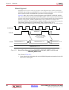
42 www.Xilinx.Com 7 series fpgas gtp transceivers user guide ug482 (v1.9) december 19, 2016 chapter 2: shared features the initializing tx must use gttxreset in sequential mode. Activating the gttxreset input can automatically trigger a full asynchronous tx reset. The reset state machine executes th...
Page 43
7 series fpgas gtp transceivers user guide www.Xilinx.Com 43 ug482 (v1.9) december 19, 2016 reset and initialization table 2-15 lists attributes required by the gtp transceiver’s tx initialization. In general cases, the reset time required by the tx pma or the tx pcs varies depending on line rate. T...
Page 44
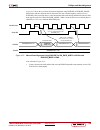
44 www.Xilinx.Com 7 series fpgas gtp transceivers user guide ug482 (v1.9) december 19, 2016 chapter 2: shared features 2. Gttxreset must be used. 3. Txpmareset and txpcsreset must be constantly driven low during the entire reset process before txresetdone is detected high. 4. Gttxreset cannot be dri...
Page 45
7 series fpgas gtp transceivers user guide www.Xilinx.Com 45 ug482 (v1.9) december 19, 2016 reset and initialization gtp transceiver tx component reset tx pma and tx pcs can be reset individually. Gttxreset must be driven constantly low during the txpmareset or txpcsreset process before finish. Driv...
Page 46
46 www.Xilinx.Com 7 series fpgas gtp transceivers user guide ug482 (v1.9) december 19, 2016 chapter 2: shared features table 2-16 summarizes all resets available to the gtp transceiver tx and components affected by them in sequential mode. Using txpmareset in sequential mode resets everything covere...
Page 47
7 series fpgas gtp transceivers user guide www.Xilinx.Com 47 ug482 (v1.9) december 19, 2016 reset and initialization after power-up and configuration the entire gtp tx requires a reset after configuration. See gtp transceiver tx reset in response to completion of configuration for the procedure. Aft...
Page 48
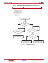
48 www.Xilinx.Com 7 series fpgas gtp transceivers user guide ug482 (v1.9) december 19, 2016 chapter 2: shared features reset state machine executes the reset sequence as shown in figure 2-18 , covering the entire rx pma and rx pcs. During normal operation, sequential mode also allows the user to ini...
Page 49
7 series fpgas gtp transceivers user guide www.Xilinx.Com 49 ug482 (v1.9) december 19, 2016 reset and initialization ports and attributes table 2-18 lists the ports required by the gtp transceiver‘s rx initialization process. X-ref target - figure 2-18 figure 2-18: gtp transceiver rx reset state mac...
Page 50
50 www.Xilinx.Com 7 series fpgas gtp transceivers user guide ug482 (v1.9) december 19, 2016 chapter 2: shared features rxosintdone out async reserved. Rxpmareset in async this port is driven high and then deasserted to start rx pma reset process. In single mode, activating rxpmareset resets only the...
Page 51
7 series fpgas gtp transceivers user guide www.Xilinx.Com 51 ug482 (v1.9) december 19, 2016 reset and initialization table 2-19 lists the attributes required by gtp transceiver’s rx initialization. In general cases, the reset time required by each reset on the rx datapath varies depending on line ra...
Page 52
52 www.Xilinx.Com 7 series fpgas gtp transceivers user guide ug482 (v1.9) december 19, 2016 chapter 2: shared features rxpmareset_time 5-bit binary reserved. Represents the time duration to apply the rx pma reset. The recommended value from the 7 series fpgas transceivers wizard should be used. Must...
Page 53
7 series fpgas gtp transceivers user guide www.Xilinx.Com 53 ug482 (v1.9) december 19, 2016 reset and initialization gtp transceiver rx reset in response to completion of configuration the rx reset sequence shown in figure 2-18 is not automatically started following the global gsr. These conditions ...
Page 54
54 www.Xilinx.Com 7 series fpgas gtp transceivers user guide ug482 (v1.9) december 19, 2016 chapter 2: shared features 4. Issue a drp write to the gtpe2_channel primitive, drpaddr 9‘h011, set bit[11] to 1’b0 . A. To ensure only bit[11] of drpaddr 9‘h011 is modified, it is best to perform a read-modi...
Page 55
7 series fpgas gtp transceivers user guide www.Xilinx.Com 55 ug482 (v1.9) december 19, 2016 reset and initialization notes relevant to figure 2-20 : 1. “drp wr” denotes the function of performing a drp write to addr 9’h011. The exact drp transaction is not shown. 2. The sequence of events in figure ...
Page 56
56 www.Xilinx.Com 7 series fpgas gtp transceivers user guide ug482 (v1.9) december 19, 2016 chapter 2: shared features gtp transceiver rx pma reset when users want to issue an rxpmareset, the steps in figure 2-21 should be performed. 1. “drp wr” denotes the function of performing a drp write to addr...
Page 57
7 series fpgas gtp transceivers user guide www.Xilinx.Com 57 ug482 (v1.9) december 19, 2016 reset and initialization table 2-20: rx component reset coverage in sequential mode functional blocks gtrx reset rxpma reset rxlpm reset eyescan reset rxpcs reset rxbuf reset rx pcs fpga rx fabric interface √...
Page 58
58 www.Xilinx.Com 7 series fpgas gtp transceivers user guide ug482 (v1.9) december 19, 2016 chapter 2: shared features table 2-22 lists the recommended resets for various situations. Table 2-21: rx component reset coverage in single mode functional blocks gtrx reset rxpma reset rxlpm reset eyescan r...
Page 59
7 series fpgas gtp transceivers user guide www.Xilinx.Com 59 ug482 (v1.9) december 19, 2016 reset and initialization after power-up and configuration the entire gtp rx requires a reset after configuration. See gtp transceiver rx reset in response to completion of configuration for procedure. After t...
Page 60
60 www.Xilinx.Com 7 series fpgas gtp transceivers user guide ug482 (v1.9) december 19, 2016 chapter 2: shared features rx rate change in most cases, in addition to changing the output divider, an rx rate change requires changing the rx cdr loop filter settings via drp (see rx cdr ). After writing in...
Page 61: Power Down
7 series fpgas gtp transceivers user guide www.Xilinx.Com 61 ug482 (v1.9) december 19, 2016 power down after changing channel bonding mode on the fly when set to true, rxbuf_reset_on_cb_change enables automatic reset of the rx elastic buffer when the rxchanbondmaster, rxchanbondslave, or rxchanbondl...
Page 62
62 www.Xilinx.Com 7 series fpgas gtp transceivers user guide ug482 (v1.9) december 19, 2016 chapter 2: shared features table 2-24 defines the power-down attributes. Txpd[1:0] in txusrclk2 (txpdelecidlemode makes this port asynchronous) powers down the tx lane according to the pci express pipe protoc...
Page 63
7 series fpgas gtp transceivers user guide www.Xilinx.Com 63 ug482 (v1.9) december 19, 2016 power down generic power-down capabilities the gtp transceiver provides several power-down features that can be used in a wide variety of applications. Table 2-25 summarizes these capabilities. Pll power down...
Page 64: Loopback
64 www.Xilinx.Com 7 series fpgas gtp transceivers user guide ug482 (v1.9) december 19, 2016 chapter 2: shared features tx and rx power down when the tx and rx power control signals are used in non pci express implementations, txpd and rxpd can be used independently. Also, when these interfaces are u...
Page 65
7 series fpgas gtp transceivers user guide www.Xilinx.Com 65 ug482 (v1.9) december 19, 2016 loopback loopback testing can be used either during development or in deployed equipment for fault isolation. The traffic patterns used can be either application traffic patterns or specialized pseudo-random ...
Page 66
66 www.Xilinx.Com 7 series fpgas gtp transceivers user guide ug482 (v1.9) december 19, 2016 chapter 2: shared features table 2-28: loopback attributes attribute type description loopback_cfg 1-bit binary reserved. Pma_loopback_cfg 1-bit binary reserved. Send feedback.
Page 67: Dynamic Reconfiguration Port
7 series fpgas gtp transceivers user guide www.Xilinx.Com 67 ug482 (v1.9) december 19, 2016 dynamic reconfiguration port dynamic reconfiguration port functional description the dynamic reconfiguration port (drp) allows the dynamic change of parameters of the gtpe2_channel and gtpe2_common primitives...
Page 68
68 www.Xilinx.Com 7 series fpgas gtp transceivers user guide ug482 (v1.9) december 19, 2016 chapter 2: shared features table 2-30: drp ports of gtpe2_common port dir clock domain description drpaddr[7:0] in drpclk drp address bus. Drpclk in n/a drp interface clock. Drpen in drpclk drp enable signal....
Page 69
7 series fpgas gtp transceivers user guide www.Xilinx.Com 69 ug482 (v1.9) december 19, 2016 dynamic reconfiguration port usage model write operation figure 2-23 shows the drp write operation timing. New drp operation can be initiated when drprdy is asserted. Read operation figure 2-24 shows the drp ...
Page 70: Digital Monitor
70 www.Xilinx.Com 7 series fpgas gtp transceivers user guide ug482 (v1.9) december 19, 2016 chapter 2: shared features digital monitor functional description the receiver uses an adaptive algorithm in optimizing a link. The digital monitor provides visibility into the convergence state of these adap...
Page 71
7 series fpgas gtp transceivers user guide www.Xilinx.Com 71 ug482 (v1.9) december 19, 2016 digital monitor ports and attributes table 2-31 shows the digital monitor ports. Table 2-32 shows the digital monitor attributes. Table 2-31: digital monitor ports port dir clock domain description dmonitorou...
Page 72
72 www.Xilinx.Com 7 series fpgas gtp transceivers user guide ug482 (v1.9) december 19, 2016 chapter 2: shared features use mode reading loop values out of the digital monitor requires a clock on input clock port dmonitorclk, change adaptation loop select through drp, and monitor output dmonitorout. ...
Page 73
7 series fpgas gtp transceivers user guide www.Xilinx.Com 73 ug482 (v1.9) december 19, 2016 digital monitor unsigned int capturedmon(unsigned int msb, unsigned int lsb); ///////// ///////////////////////////////////////////////// // initialize digital monitor ////////////////////////////////////////...
Page 74
74 www.Xilinx.Com 7 series fpgas gtp transceivers user guide ug482 (v1.9) december 19, 2016 chapter 2: shared features send feedback.
Page 75: Transmitter
7 series fpgas gtp transceivers user guide www.Xilinx.Com 75 ug482 (v1.9) december 19, 2016 chapter 3 transmitter tx overview functional description this chapter shows how to configure and use each of the functional blocks inside the transmitter (tx). Each transceiver includes an independent transmi...
Page 76: Fpga Tx Interface
76 www.Xilinx.Com 7 series fpgas gtp transceivers user guide ug482 (v1.9) december 19, 2016 chapter 3: transmitter 5. Tx pattern generator, page 103 6. Tx pattern generator, page 103 7. Tx polarity control, page 106 8. Tx fabric clock output control, page 107 9. Tx configurable driver, page 114 10. ...
Page 77
7 series fpgas gtp transceivers user guide www.Xilinx.Com 77 ug482 (v1.9) december 19, 2016 fpga tx interface txusrclk and txusrclk2 generation the fpga tx interface includes two parallel clocks: txusrclk and txusrclk2. Txusrclk is the internal clock for the pcs logic in the gtp transceiver transmit...
Page 78
78 www.Xilinx.Com 7 series fpgas gtp transceivers user guide ug482 (v1.9) december 19, 2016 chapter 3: transmitter table 3-5 defines the fpga tx interface attributes. Using txoutclk to drive the tx interface depending on the txusrclk and txusrclk2 frequencies, there are different ways fpga clock res...
Page 79
7 series fpgas gtp transceivers user guide www.Xilinx.Com 79 ug482 (v1.9) december 19, 2016 fpga tx interface txoutclk driving gtp transceiver tx in 2-byte mode in figure 3-2 , txoutclk is used to drive txusrclk and txusrclk2 for 2-byte mode (tx_data_width = 16 or 20) in a single-lane configuration....
Page 80
80 www.Xilinx.Com 7 series fpgas gtp transceivers user guide ug482 (v1.9) december 19, 2016 chapter 3: transmitter similarly, figure 3-3 shows the shows the same settings in multiple lanes configuration. Notes relevant to figure 3-3 : 1. Bufh can be used with certain limitations. For details about p...
Page 81
7 series fpgas gtp transceivers user guide www.Xilinx.Com 81 ug482 (v1.9) december 19, 2016 fpga tx interface txoutclk driving gtp transceiver tx in 4-byte mode in figure 3-4 , txoutclk is used to drive txusrclk2 for 4-byte mode (tx_data_width = 32 or 40). The frequency of txusrclk2 is equal to half...
Page 82
82 www.Xilinx.Com 7 series fpgas gtp transceivers user guide ug482 (v1.9) december 19, 2016 chapter 3: transmitter similarly, figure 3-5 shows the shows the same settings in multiple lanes configuration. Notes relevant to figure 3-5 : 1. F txusrclk2 = f txusrclk /2. 2. In the xc7a200t device, bufh c...
Page 83: Tx 8B/10B Encoder
7 series fpgas gtp transceivers user guide www.Xilinx.Com 83 ug482 (v1.9) december 19, 2016 tx 8b/10b encoder tx 8b/10b encoder functional description many protocols use 8b/10b encoding on outgoing data. 8b/10b is an industry standard encoding scheme that trades two bits overhead per byte for achiev...
Page 84
84 www.Xilinx.Com 7 series fpgas gtp transceivers user guide ug482 (v1.9) december 19, 2016 chapter 3: transmitter running disparity 8b/10b coding is dc-balanced, meaning that the long-term ratio of 1s and 0s transmitted should be exactly 50%. To achieve this, the encoder always calculates the diffe...
Page 85
7 series fpgas gtp transceivers user guide www.Xilinx.Com 85 ug482 (v1.9) december 19, 2016 tx 8b/10b encoder ports and attributes table 3-7 lists the ports required by the tx 8b/10b encoder. Note: there are no tx encoder attributes. Table 3-7: tx 8b/10b encoder ports port dir clock domain descripti...
Page 86: Tx Gearbox
86 www.Xilinx.Com 7 series fpgas gtp transceivers user guide ug482 (v1.9) december 19, 2016 chapter 3: transmitter enabling and disabling 8b/10b encoding to enable the 8b/10b encoder, tx8b10ben must be driven high. The tx 8b/10b encoder allows byte interleaved data to bypass the encoder on a per-byt...
Page 87
7 series fpgas gtp transceivers user guide www.Xilinx.Com 87 ug482 (v1.9) december 19, 2016 tx gearbox table 3-9 defines the tx gearbox attributes. Enabling the tx gearbox to enable the tx gearbox for the gtp transceiver, set the attribute txgearbox_en to true. The gearbox_mode attribute controls th...
Page 88
88 www.Xilinx.Com 7 series fpgas gtp transceivers user guide ug482 (v1.9) december 19, 2016 chapter 3: transmitter note relevant to figure 3-7 : 1. Per ieee802.3ae nomenclature, h1 corresponds to txb, h0 to txb, etc. X-ref target - figure 3-7 figure 3-7: tx gearbox bit ordering ug482_c3_07_110911 h1...
Page 89
7 series fpgas gtp transceivers user guide www.Xilinx.Com 89 ug482 (v1.9) december 19, 2016 tx gearbox tx gearbox operating modes the gtp transceiver's tx gearbox only supports the external sequence counter mode and this must be implemented in user logic. The tx gearbox supports 2-byte and 4-byte in...
Page 90
90 www.Xilinx.Com 7 series fpgas gtp transceivers user guide ug482 (v1.9) december 19, 2016 chapter 3: transmitter due to the nature of the 64b/66b and 64b/67b encoding schemes, user data is held (paused) during various sequence counter values. Data is paused for two txusrclk2 cycles in 2-byte mode ...
Page 91
7 series fpgas gtp transceivers user guide www.Xilinx.Com 91 ug482 (v1.9) december 19, 2016 tx gearbox figure 3-9 shows how a pause occurs at counter value 31 when using an 4-byte fabric interface in external sequence counter mode with 64b/66b encoding. Figure 3-10 shows how a pause occurs at counte...
Page 92
92 www.Xilinx.Com 7 series fpgas gtp transceivers user guide ug482 (v1.9) december 19, 2016 chapter 3: transmitter 9. On count 45, drive data on txdata. 10. On count 65, stop data pipeline. 11. On count 66, drive data on txdata. The sequence of transmitting 64/66 data for the external sequence count...
Page 93: Tx Buffer
7 series fpgas gtp transceivers user guide www.Xilinx.Com 93 ug482 (v1.9) december 19, 2016 tx buffer tx buffer functional description the gtp transceiver tx datapath has two internal parallel clock domains used in the pcs: the pma parallel clock domain (xclk) and the txusrclk domain. To transmit da...
Page 94
94 www.Xilinx.Com 7 series fpgas gtp transceivers user guide ug482 (v1.9) december 19, 2016 chapter 3: transmitter ports and attributes table 3-13 defines the tx buffer ports. Table 3-14 defines the tx buffer attributes. Table 3-12: tx buffering versus phase alignment tx buffer tx phase alignment ea...
Page 95: Tx Buffer Bypass
7 series fpgas gtp transceivers user guide www.Xilinx.Com 95 ug482 (v1.9) december 19, 2016 tx buffer bypass using the tx buffer the tx buffer should be reset whenever txbufstatus indicates an overflow or underflow condition. The tx buffer can be reset by using gttxreset, txpcsreset, or the gtp tran...
Page 96
96 www.Xilinx.Com 7 series fpgas gtp transceivers user guide ug482 (v1.9) december 19, 2016 chapter 3: transmitter table 3-15: tx buffer bypass ports port dir clock domain description txphdlyreset in async tx phase alignment hard reset. Forces txoutclk to the center of the delay alignment tap. The d...
Page 97
7 series fpgas gtp transceivers user guide www.Xilinx.Com 97 ug482 (v1.9) december 19, 2016 tx buffer bypass txphinitdone out async indicates that tx phase alignment initialization is done. Txdlysresetdone out async indicates that tx delay alignment soft reset is done. Txsyncmode in async reserved. ...
Page 98
98 www.Xilinx.Com 7 series fpgas gtp transceivers user guide ug482 (v1.9) december 19, 2016 chapter 3: transmitter tx buffer bypass use modes tx phase alignment can be performed on one channel (single lane) or a group of channels sharing a single txoutclk (multi-lane). For gtp transceivers, tx buffe...
Page 99
7 series fpgas gtp transceivers user guide www.Xilinx.Com 99 ug482 (v1.9) december 19, 2016 tx buffer bypass figure 3-12 shows the required steps to perform the tx phase alignment and use the tx delay alignment to adjust txusrclk to compensate for temperature and voltage variations. Notes relevant t...
Page 100
100 www.Xilinx.Com 7 series fpgas gtp transceivers user guide ug482 (v1.9) december 19, 2016 chapter 3: transmitter using tx buffer bypass in multi-lane mode this section describes the steps required to perform the multi-lane tx buffer bypass alignment procedure. • master: in a multi-lane applicatio...
Page 101
7 series fpgas gtp transceivers user guide www.Xilinx.Com 101 ug482 (v1.9) december 19, 2016 tx buffer bypass figure 3-14 shows an example of buffer bypass master versus slave lanes. These gtp transceiver settings are used to bypass the tx buffer: • txbuf_en = false • tx_xclk_sel = txusr • txoutclks...
Page 102
102 www.Xilinx.Com 7 series fpgas gtp transceivers user guide ug482 (v1.9) december 19, 2016 chapter 3: transmitter figure 3-15 shows the required steps to perform tx phase and delay alignment. Notes relevant to figure 3-15 : 1. The sequence of events shown in figure 3-15 is not drawn to scale. 2. M...
Page 103: Tx Pattern Generator
7 series fpgas gtp transceivers user guide www.Xilinx.Com 103 ug482 (v1.9) december 19, 2016 tx pattern generator 15. Deassert txdlyen for the master lane. 16. Assert txphinit for all slave lane(s). Hold this signal high until the rising edge of txphinitdone of the respective slave lane is observed....
Page 104
104 www.Xilinx.Com 7 series fpgas gtp transceivers user guide ug482 (v1.9) december 19, 2016 chapter 3: transmitter the error insertion function is supported to verify link connection and also for jitter tolerance tests. When an inverted prbs pattern is necessary, the txpolarity signal is used to co...
Page 105
7 series fpgas gtp transceivers user guide www.Xilinx.Com 105 ug482 (v1.9) december 19, 2016 tx pattern generator table 3-21 defines the pattern generator attribute. Use models the pattern generation and check function are usually used for verifying link quality tests and also for jitter tolerance t...
Page 106: Tx Polarity Control
106 www.Xilinx.Com 7 series fpgas gtp transceivers user guide ug482 (v1.9) december 19, 2016 chapter 3: transmitter to calculate accurately the receiver’s bit error rate (ber), an external jitter tolerance tester should be used. For the test, the gtp transceiver should loop the received error status...
Page 107
7 series fpgas gtp transceivers user guide www.Xilinx.Com 107 ug482 (v1.9) december 19, 2016 tx fabric clock output control ports and attributes table 3-22 defines the ports required for tx polarity control. Using tx polarity control txpolarity can be tied high if the polarity of txp and txn needs t...
Page 108
108 www.Xilinx.Com 7 series fpgas gtp transceivers user guide ug482 (v1.9) december 19, 2016 chapter 3: transmitter notes relevant to figure 3-20 : 1. Txoutclkpcs and txoutclkfabric are redundant outputs. Use txoutclk for new designs. 2. The refclk_ctrl option is controlled automatically by software...
Page 109
7 series fpgas gtp transceivers user guide www.Xilinx.Com 109 ug482 (v1.9) december 19, 2016 tx fabric clock output control serial clock divider each transmitter pma module has a d divider that divides down the clock from the pll for lower line rate support. This serial clock divider, d, can be set ...
Page 110
110 www.Xilinx.Com 7 series fpgas gtp transceivers user guide ug482 (v1.9) december 19, 2016 chapter 3: transmitter ports and attributes table 3-24 defines the ports required for tx fabric clock output control. Table 3-24: tx fabric clock output control ports port dir clock domain description txoutc...
Page 111
7 series fpgas gtp transceivers user guide www.Xilinx.Com 111 ug482 (v1.9) december 19, 2016 tx phase interpolator ppm controller table 3-25 defines the attributes required for tx fabric clock output control. Tx phase interpolator ppm controller functional description the tx phase interpolator parts...
Page 112
112 www.Xilinx.Com 7 series fpgas gtp transceivers user guide ug482 (v1.9) december 19, 2016 chapter 3: transmitter ports and attributes table 3-26 defines the ports required for the tx phase interpolator ppm controller. Table 3-27 defines the attributes required for the tx phase interpolator ppm co...
Page 113
7 series fpgas gtp transceivers user guide www.Xilinx.Com 113 ug482 (v1.9) december 19, 2016 tx phase interpolator ppm controller tx phase interpolator ppm controller use mode the following describes a sample use case: • a frequency counter in the fabric determines the lead/lag relationship between ...
Page 114: Tx Configurable Driver
114 www.Xilinx.Com 7 series fpgas gtp transceivers user guide ug482 (v1.9) december 19, 2016 chapter 3: transmitter tx configurable driver functional description the gtp transceiver tx driver is a high-speed current-mode differential output buffer. To maximize signal integrity, it includes these fea...
Page 115
7 series fpgas gtp transceivers user guide www.Xilinx.Com 115 ug482 (v1.9) december 19, 2016 tx configurable driver txdiffctrl[3:0] in async driver swing control. The default is user specified. All listed values are in mv ppd . Txelecidle in txusrclk2 when high, this signal forces gtptxp and gtptxn ...
Page 116
116 www.Xilinx.Com 7 series fpgas gtp transceivers user guide ug482 (v1.9) december 19, 2016 chapter 3: transmitter txmargin[2:0] in async tx margin control for pci express pipe 2.0 interface. These signals are mapped internally to txdiffctrl/txbufdiffctrl via attributes. Pmarsvdin1 in async reserve...
Page 117
7 series fpgas gtp transceivers user guide www.Xilinx.Com 117 ug482 (v1.9) december 19, 2016 tx configurable driver txpostcursor[4:0] in async transmitter post-cursor tx pre-emphasis control. The default is user specified. All listed values (db) are typical. Txpostcursorinv in async when set to 1'b1...
Page 118
118 www.Xilinx.Com 7 series fpgas gtp transceivers user guide ug482 (v1.9) december 19, 2016 chapter 3: transmitter txprecursor[4:0] in async transmitter pre-cursor tx pre-emphasis control. The default is user specified. All listed values (db) are typical. Txprecursorinv in async when set to 1'b1, i...
Page 119
7 series fpgas gtp transceivers user guide www.Xilinx.Com 119 ug482 (v1.9) december 19, 2016 tx configurable driver table 3-29 defines the tx configurable driver attributes. Mgtptxp mgtptxn out (pad) tx serial clock mgtptxp and mgtptxn are differential complements of one another forming a differenti...
Page 120
120 www.Xilinx.Com 7 series fpgas gtp transceivers user guide ug482 (v1.9) december 19, 2016 chapter 3: transmitter tx_margin_full_2[6:0] 7-bit binary this attribute has the value of txbufdiffctrl[2:0] and txdiffctrl[3:0] that has to be mapped when txmargin = 010 and txswing = 0. Tx_margin_full_0 = ...
Page 121
7 series fpgas gtp transceivers user guide www.Xilinx.Com 121 ug482 (v1.9) december 19, 2016 tx receiver detect support for pci express designs tx receiver detect support for pci express designs functional description the pci express specification includes a feature that allows the transmitter on a ...
Page 122
122 www.Xilinx.Com 7 series fpgas gtp transceivers user guide ug482 (v1.9) december 19, 2016 chapter 3: transmitter using the tx receiver detection for pci express while in the p1 power state, the gtp transceiver can be instructed to perform a receiver detection operation to determine if there is a ...
Page 123: Tx Out-of-Band Signaling
7 series fpgas gtp transceivers user guide www.Xilinx.Com 123 ug482 (v1.9) december 19, 2016 tx out-of-band signaling note: figure 3-23 shows the sequence of events for the receiver present case and is not drawn to scale. Notes relevant to figure 3-23 : 1. Ensure that the gtp transceiver has success...
Page 124
124 www.Xilinx.Com 7 series fpgas gtp transceivers user guide ug482 (v1.9) december 19, 2016 chapter 3: transmitter table 3-33 shows the oob signaling attributes. Txpdelecidlemode in txusrclk2 determines if txelecidle and txpd should be treated as synchronous or asynchronous signals. Enables complia...
Page 125: Receiver
7 series fpgas gtp transceivers user guide www.Xilinx.Com 125 ug482 (v1.9) december 19, 2016 chapter 4 receiver rx overview functional description this section shows how to configure and use each of the functional blocks inside the receiver (rx). Each gtp transceiver includes an independent receiver...
Page 126: Rx Analog Front End
126 www.Xilinx.Com 7 series fpgas gtp transceivers user guide ug482 (v1.9) december 19, 2016 chapter 4: receiver 9. Rx byte and word alignment, page 161 10. Rx 8b/10b decoder, page 170 11. Rx buffer bypass, page 174 12. Rx elastic buffer, page 187 13. Rx clock correction, page 191 14. Rx channel bon...
Page 127
7 series fpgas gtp transceivers user guide www.Xilinx.Com 127 ug482 (v1.9) december 19, 2016 rx analog front end ports and attributes table 4-1 defines the rx afe ports. Table 4-2 defines the rx afe attributes. Table 4-1: rx afe ports port dir clock domain description gtprxn, gtprxp in (pad) rx seri...
Page 128
128 www.Xilinx.Com 7 series fpgas gtp transceivers user guide ug482 (v1.9) december 19, 2016 chapter 4: receiver use modes—rx termination term_rcal_ovrd 3-bit binary selects whether the external 100 Ω precision resistor connected to the mgtrref pin or an override value is used, as defined by term_rc...
Page 129
7 series fpgas gtp transceivers user guide www.Xilinx.Com 129 ug482 (v1.9) december 19, 2016 rx analog front end table 4-4: use mode 2—rx termination use mode external ac coupling term voltage max swing mv dpp suggested protocols and usage notes 2 on avtt 1,200 protocols: • backplane • cei-6 (1,200 ...
Page 130
130 www.Xilinx.Com 7 series fpgas gtp transceivers user guide ug482 (v1.9) december 19, 2016 chapter 4: receiver table 4-5: use mode 3—rx termination use mode external ac coupling term voltage max swing mv dpp suggested protocols and usage notes 3 on 800 mv 2,000 protocols: • optical if (sonet/sdh/o...
Page 131: Rx Out-of-Band Signaling
7 series fpgas gtp transceivers user guide www.Xilinx.Com 131 ug482 (v1.9) december 19, 2016 rx out-of-band signaling rx out-of-band signaling functional description the gtp transceiver receiver provides support for decoding the out-of-band (oob) sequences described in the serial ata (sata) and seri...
Page 132
132 www.Xilinx.Com 7 series fpgas gtp transceivers user guide ug482 (v1.9) december 19, 2016 chapter 4: receiver use mode to use oob, the following rx termination conditions need to be applied: • ac-coupled case: termination voltage should be 800 mv or greater • dc-coupled case: termination voltage ...
Page 133
7 series fpgas gtp transceivers user guide www.Xilinx.Com 133 ug482 (v1.9) december 19, 2016 rx out-of-band signaling also, the attribute pcs_rsvd_attr[8] should be set to 1'b1. The oob circuit has two possible sources from which it can receive a clock, as shown in figure 4-6 . The attribute rxoob_c...
Page 134
134 www.Xilinx.Com 7 series fpgas gtp transceivers user guide ug482 (v1.9) december 19, 2016 chapter 4: receiver figure 4-8 shows how cascading several divide-by-two circuits produces higher order clock dividers such as divide-by-4 and divide-by-8. Use modes for oob operating at a line rate of 1.5 g...
Page 135
7 series fpgas gtp transceivers user guide www.Xilinx.Com 135 ug482 (v1.9) december 19, 2016 rx out-of-band signaling table 4-8: oob guidelines for operating rates above 1.5 gb/s protocol operation pcie gen1 see figure 4-10 for the algorithm to determine whether the rx is in electrical idle. If a sc...
Page 136
136 www.Xilinx.Com 7 series fpgas gtp transceivers user guide ug482 (v1.9) december 19, 2016 chapter 4: receiver notes: 1. The attributes pertaining to lpm, and cdr are: • rxcdr_hold_during_eidle • rxcdr_fr_reset_on_eidle • rxcdr_ph_reset_on_eidle • rx_lpm_hold_during_eidle • rxbuf_reset_on_eidle • ...
Page 137
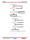
7 series fpgas gtp transceivers user guide www.Xilinx.Com 137 ug482 (v1.9) december 19, 2016 rx out-of-band signaling x-ref target - figure 4-11 figure 4-11: flowchart for pcie gen2 x-ref target - figure 4-12 figure 4-12: flowchart for entry to rx electrical idle for pcie gen2 rx is in electrical id...
Page 138
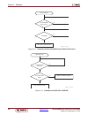
138 www.Xilinx.Com 7 series fpgas gtp transceivers user guide ug482 (v1.9) december 19, 2016 chapter 4: receiver x-ref target - figure 4-13 figure 4-13: flowchart for exit from rx electrical idle for pcie gen2 x-ref target - figure 4-14 figure 4-14: flowchart for sata 3g or sata 6g rx is out of elec...
Page 139: Rx Equalizer
7 series fpgas gtp transceivers user guide www.Xilinx.Com 139 ug482 (v1.9) december 19, 2016 rx equalizer rx equalizer functional description the gtp transceiver receiver has a power-efficient adaptive continuous time linear equalizer (ctle) to compensate for signal distortion due to high-frequency ...
Page 140
140 www.Xilinx.Com 7 series fpgas gtp transceivers user guide ug482 (v1.9) december 19, 2016 chapter 4: receiver table 4-10: rx equalizer attributes attribute type description adapt_cfg0 20-bit binary reserved. The recommended value from the 7 series fpgas transceivers wizard should be used. Rx_lpm_...
Page 141: Rx Cdr
7 series fpgas gtp transceivers user guide www.Xilinx.Com 141 ug482 (v1.9) december 19, 2016 rx cdr rx cdr functional description the rx clock data recovery (cdr) circuit in each gtpe2_channel transceiver extracts the recovered clock and data from an incoming data stream. Figure 4-16 illustrates the...
Page 142
142 www.Xilinx.Com 7 series fpgas gtp transceivers user guide ug482 (v1.9) december 19, 2016 chapter 4: receiver ports and attributes table 4-11 defines the cdr ports. Table 4-11: cdr ports port dir clock domain description rxcdrfreqreset in async reserved. Tied low. Rxcdrhold in async hold the cdr ...
Page 143
7 series fpgas gtp transceivers user guide www.Xilinx.Com 143 ug482 (v1.9) december 19, 2016 rx cdr table 4-12 defines the cdr related attributes. Rxosintstrobe in async reserved. The recommended value from the 7 series fpgas transceivers wizard should be used. Rxosinthold in async reserved. The rec...
Page 144
144 www.Xilinx.Com 7 series fpgas gtp transceivers user guide ug482 (v1.9) december 19, 2016 chapter 4: receiver use modes rx cdr lock to reference to get the cdr to lock to reference set rxcdrhold = 1'b1 and set rxcdrovrden = 1'b0 dynamically changing rx cdr settings for line rate and selected prot...
Page 145
7 series fpgas gtp transceivers user guide www.Xilinx.Com 145 ug482 (v1.9) december 19, 2016 rx cdr 2 ±200 83'h0_0011_07fe_2060_2108_1010 ±700 ±1,250 4 or 8 ±200 83'h0_0011_07fe_0860_2110_1010 ±700 ±1,250 notes: 1. For protocol-specific settings, use the recommended value from the 7 series fpgas tra...
Page 146
146 www.Xilinx.Com 7 series fpgas gtp transceivers user guide ug482 (v1.9) december 19, 2016 chapter 4: receiver rx fabric clock output control functional description the rx clock divider control block has two main components: serial clock divider control and parallel clock divider and selector cont...
Page 147
7 series fpgas gtp transceivers user guide www.Xilinx.Com 147 ug482 (v1.9) december 19, 2016 rx fabric clock output control 5. For details about placement constraints and restrictions on clocking resources (mmcme2, plle2, ibufds_gte2, bufg, etc.), refer to ug472 , 7 series fpgas clocking resources u...
Page 148
148 www.Xilinx.Com 7 series fpgas gtp transceivers user guide ug482 (v1.9) december 19, 2016 chapter 4: receiver clock), to clock the downstream fabric logic. It is also used by the rx pcs block. This clock is interrupted when the pll or cdr is reset by one of the related reset signals. • rxoutclkse...
Page 149
7 series fpgas gtp transceivers user guide www.Xilinx.Com 149 ug482 (v1.9) december 19, 2016 rx fabric clock output control table 4-18 defines the attributes required for rx fabric clock output control. Using rxrate when users want to change the divider d setting via rxrate, the steps in figure 4-19...
Page 150: Rx Margin Analysis
150 www.Xilinx.Com 7 series fpgas gtp transceivers user guide ug482 (v1.9) december 19, 2016 chapter 4: receiver 2. The sequence of events in figure 4-19 is not drawn to scale. 3. To change rxrate, a drp write must be issued to the gtpe2_channel primitive, drpaddr 9'h011, set bit[11] to 1'b0. A. To ...
Page 151
7 series fpgas gtp transceivers user guide www.Xilinx.Com 151 ug482 (v1.9) december 19, 2016 rx margin analysis eye scan theory rxdata is recovered from the equalized differential waveform by sampling after the rx equalizer. The horizontal sampling position is determined by the cdr function and the ...
Page 152
152 www.Xilinx.Com 7 series fpgas gtp transceivers user guide ug482 (v1.9) december 19, 2016 chapter 4: receiver figure 4-22 describes the portion of the pcs architecture that supports eye scan. The 40-bit rdata bus contains the data samples, and each bit of the 40-bit sdata bus is one if and only i...
Page 153
7 series fpgas gtp transceivers user guide www.Xilinx.Com 153 ug482 (v1.9) december 19, 2016 rx margin analysis the diagnostic use modes could be used, for example, to examine the pattern of burst errors due to equalization behavior. Figure 4-23 documents the state transitions in the eye scan state ...
Page 154
154 www.Xilinx.Com 7 series fpgas gtp transceivers user guide ug482 (v1.9) december 19, 2016 chapter 4: receiver ports and attributes table 4-19 defines ports related to the rx eye scan function. Table 4-20 defines rx eye scan attributes. Lower case attribute names indicate r/o. Table 4-19: rx margi...
Page 155
7 series fpgas gtp transceivers user guide www.Xilinx.Com 155 ug482 (v1.9) december 19, 2016 rx margin analysis es_sdata_mask 80-bit hex this attribute masks up to two cycles of the 40-bit sdata bus. Binary 1 causes the corresponding bus bit to be masked and binary 0 leaves it unmasked. To support t...
Page 156
156 www.Xilinx.Com 7 series fpgas gtp transceivers user guide ug482 (v1.9) december 19, 2016 chapter 4: receiver es_control 6-bit binary [0]: run. Asserting this bit causes a state transition from the wait state to the reset state, initiating a ber measurement sequence. [1]: arm asserting this bit c...
Page 157: Rx Polarity Control
7 series fpgas gtp transceivers user guide www.Xilinx.Com 157 ug482 (v1.9) december 19, 2016 rx polarity control rx polarity control functional description if rxp and rxn differential traces are accidentally swapped on the pcb, the differential data received by the gtp transceiver rx are reversed. T...
Page 158: Rx Pattern Checker
158 www.Xilinx.Com 7 series fpgas gtp transceivers user guide ug482 (v1.9) december 19, 2016 chapter 4: receiver using rx polarity control rxpolarity can be tied high if the polarity of rxp and rxn needs to be reversed. Rx pattern checker functional description the gtp transceiver receiver includes ...
Page 159
7 series fpgas gtp transceivers user guide www.Xilinx.Com 159 ug482 (v1.9) december 19, 2016 rx pattern checker ports and attributes table 4-23 defines the pattern checker ports. Table 4-24 defines the pattern checker attributes. Use models to use the built-in prbs checker, rxprbssel must be set to ...
Page 160: Rx Byte and Word Alignment
160 www.Xilinx.Com 7 series fpgas gtp transceivers user guide ug482 (v1.9) december 19, 2016 chapter 4: receiver inverted by controlling rxpolarity. Otherwise, the prbs checker does not lock. When it finds the pattern, it can detect prbs errors by comparing the incoming pattern with the expected pat...
Page 161
7 series fpgas gtp transceivers user guide www.Xilinx.Com 161 ug482 (v1.9) december 19, 2016 rx byte and word alignment figure 4-26 shows tx parallel data on the left side, and rx receiving recognizable parallel data after comma alignment on the right side. Enabling comma alignment to enable the com...
Page 162
162 www.Xilinx.Com 7 series fpgas gtp transceivers user guide ug482 (v1.9) december 19, 2016 chapter 4: receiver figure 4-29 shows how a comma is combined with align_comma_enable to make a wild-carded comma for a 20-bit internal comma. If align_comma_double is true, the mcomma and pcomma patterns ar...
Page 163
7 series fpgas gtp transceivers user guide www.Xilinx.Com 163 ug482 (v1.9) december 19, 2016 rx byte and word alignment boundary. In such applications, rxbyteisaligned should not be used as a valid indicator of the change in byte boundary after the first assertion. Alignment boundaries the allowed b...
Page 164
164 www.Xilinx.Com 7 series fpgas gtp transceivers user guide ug482 (v1.9) december 19, 2016 chapter 4: receiver manual alignment rxslide can be used to override the automatic comma alignment and to shift the parallel data. Rxslide is driven high for one rxusrclk2 cycle to shift the parallel data by...
Page 165
7 series fpgas gtp transceivers user guide www.Xilinx.Com 165 ug482 (v1.9) december 19, 2016 rx byte and word alignment figure 4-32 shows the waveforms for manual alignment using rxslide in rxslide_mode = pma before and after the data shift. In this mode, the data is shifted right by one bit for eve...
Page 166
166 www.Xilinx.Com 7 series fpgas gtp transceivers user guide ug482 (v1.9) december 19, 2016 chapter 4: receiver ports and attributes table 4-25 defines the rx byte and word alignment ports. Table 4-25: rx byte and word alignment ports port name dir clock domain description rxbyteisaligned out rxusr...
Page 167
7 series fpgas gtp transceivers user guide www.Xilinx.Com 167 ug482 (v1.9) december 19, 2016 rx byte and word alignment table 4-26 defines the rx byte and word alignment attributes. Rxslide in rxusrclk2 rxslide implements a comma alignment bump control. When rxslide is asserted, the byte alignment i...
Page 168
168 www.Xilinx.Com 7 series fpgas gtp transceivers user guide ug482 (v1.9) december 19, 2016 chapter 4: receiver align_comma_double string specifies whether a comma match consists of either a comma plus or a comma minus alone, or if both are required in the sequence. False: the plus comma (pcomma) a...
Page 169: Rx 8B/10B Decoder
7 series fpgas gtp transceivers user guide www.Xilinx.Com 169 ug482 (v1.9) december 19, 2016 rx 8b/10b decoder rx 8b/10b decoder functional description if rx received data is 8b/10b encoded, it must be decoded. The gtp transceiver has a built-in 8b/10b encoder in the gtp transceiver tx and an 8b/10b...
Page 170
170 www.Xilinx.Com 7 series fpgas gtp transceivers user guide ug482 (v1.9) december 19, 2016 chapter 4: receiver transceiver always receives the right-most bit first. Consequently, the 8b/10b decoder automatically reverses the bit order of received data before decoding it. Decoded data is available ...
Page 171
7 series fpgas gtp transceivers user guide www.Xilinx.Com 171 ug482 (v1.9) december 19, 2016 rx 8b/10b decoder • the corresponding rxdisperr represents the 9th bit • the corresponding rxcharisk represents the 8th bit • the corresponding rxdata byte represents the [7:0] bits figure 4-34 shows a wavef...
Page 172
172 www.Xilinx.Com 7 series fpgas gtp transceivers user guide ug482 (v1.9) december 19, 2016 chapter 4: receiver ports and attributes table 4-27 defines the ports required by rx 8b/10b decoder. Table 4-27: rx 8b/10b decoder ports port dir clock domain description rx8b10ben in rxusrclk2 rx8b10ben sel...
Page 173: Rx Buffer Bypass
7 series fpgas gtp transceivers user guide www.Xilinx.Com 173 ug482 (v1.9) december 19, 2016 rx buffer bypass enabling and disabling 8b/10b decoding to enable the 8b/10b decoder, rx8b10ben must be driven high. Rx_data_width must be set to a multiple of 8 (8, 16, 32) when the 8b/10b decoder enabled. ...
Page 174
174 www.Xilinx.Com 7 series fpgas gtp transceivers user guide ug482 (v1.9) december 19, 2016 chapter 4: receiver when rx buffer bypass is used, rxslide_mode cannot be set to auto or pma. Ports and attributes table 4-29 defines the rx buffer bypass ports. X-ref target - figure 4-35 figure 4-35: using...
Page 175
7 series fpgas gtp transceivers user guide www.Xilinx.Com 175 ug482 (v1.9) december 19, 2016 rx buffer bypass rxphdlypd in async rx phase and delay alignment circuit power down. Tied high when a) rx buffer bypass is not in use; b) rxpd is asserted or c) rxoutclksel is set to 3'b010 but the recovered...
Page 176
176 www.Xilinx.Com 7 series fpgas gtp transceivers user guide ug482 (v1.9) december 19, 2016 chapter 4: receiver table 4-30 defines the rx buffer attributes. Rxphaligndone out async rx phase alignment done. When the auto rx phase and delay alignment are used, the second rising edge of rxphaligndone ...
Page 177
7 series fpgas gtp transceivers user guide www.Xilinx.Com 177 ug482 (v1.9) december 19, 2016 rx buffer bypass rx_xclk_sel string selects the clock source used to drive the rx parallel clock domain (xclk). Rxrec: selects the rx recovered clock as source of xclk. Used when using the rx elastic buffer....
Page 178
178 www.Xilinx.Com 7 series fpgas gtp transceivers user guide ug482 (v1.9) december 19, 2016 chapter 4: receiver rx buffer bypass use modes rx phase alignment can be performed on one channel (single lane) or a group of channels sharing a single rxoutclk (multi-lane). For gtp transceivers, rx buffer ...
Page 179
7 series fpgas gtp transceivers user guide www.Xilinx.Com 179 ug482 (v1.9) december 19, 2016 rx buffer bypass figure 4-37 shows the required steps to perform the auto rx phase alignment and use the rx delay alignment to adjust rxusrclk to compensate for temperature and voltage variations. Notes rele...
Page 180
180 www.Xilinx.Com 7 series fpgas gtp transceivers user guide ug482 (v1.9) december 19, 2016 chapter 4: receiver using rx buffer bypass in multi-lane manual mode for gtp transceivers, phase alignment can be performed manually or automatically. This section describes the steps required to perform the...
Page 181
7 series fpgas gtp transceivers user guide www.Xilinx.Com 181 ug482 (v1.9) december 19, 2016 rx buffer bypass • resetting or powering up the pll • changing the rx recovered clock source or frequency • changing the gtp transceiver rx line rate figure 4-39 shows the required steps to perform manual rx...
Page 182
182 www.Xilinx.Com 7 series fpgas gtp transceivers user guide ug482 (v1.9) december 19, 2016 chapter 4: receiver 13. Deassert rxdlyen for the master lane. 14. Assert rxphalign for all slave lane(s). Hold this signal high until the rising edge of rxphaligndone of the respective slave lane is observed...
Page 183
7 series fpgas gtp transceivers user guide www.Xilinx.Com 183 ug482 (v1.9) december 19, 2016 rx buffer bypass these gtp transceiver settings should be used to bypass the rx buffer: • rxbuf_en = false. • rx_xclk_sel = rxusr. • rxoutclksel = 010 to select the rx recovered clock as the source of rxoutc...
Page 184
184 www.Xilinx.Com 7 series fpgas gtp transceivers user guide ug482 (v1.9) december 19, 2016 chapter 4: receiver figure 4-42 shows the required steps to perform auto rx phase and delay alignment. X-ref target - figure 4-41 figure 4-41: rx buffer bypass—multi-lane auto mode port connection ug482_c4_1...
Page 185
7 series fpgas gtp transceivers user guide www.Xilinx.Com 185 ug482 (v1.9) december 19, 2016 rx buffer bypass notes relevant to figure 4-42 : 1. The sequence of events shown in figure 4-42 is not drawn to scale. 2. M_* denotes ports related to the master lane. 3. S_* denotes ports related to the sla...
Page 186: Rx Elastic Buffer
186 www.Xilinx.Com 7 series fpgas gtp transceivers user guide ug482 (v1.9) december 19, 2016 chapter 4: receiver it is necessary to start the rx phase alignment after rx cdr is locked to ensure that the rx recovered clock and rxusrclk are stable and ready to be used for alignment. When the rx elasti...
Page 187
7 series fpgas gtp transceivers user guide www.Xilinx.Com 187 ug482 (v1.9) december 19, 2016 rx elastic buffer ports and attributes table 4-33 defines the rx buffer ports. Table 4-34 defines the rx buffer attributes. Table 4-32: rx buffering versus phase alignment rx elastic buffer rx phase alignmen...
Page 188
188 www.Xilinx.Com 7 series fpgas gtp transceivers user guide ug482 (v1.9) december 19, 2016 chapter 4: receiver rx_buffer_cfg 6-bit binary rx elastic buffer configuration. Reserved. The recommended value from the 7 series fpgas transceivers wizard should be used. Rx_defer_reset_buf_en string defer ...
Page 189
7 series fpgas gtp transceivers user guide www.Xilinx.Com 189 ug482 (v1.9) december 19, 2016 rx elastic buffer using the rx elastic buffer these settings are used to enable the rx elastic buffer to resolve phase differences between the xclk and rxusrclk domains: • rxbuf_en = true • rx_xclk_sel = rxr...
Page 190: Rx Clock Correction
190 www.Xilinx.Com 7 series fpgas gtp transceivers user guide ug482 (v1.9) december 19, 2016 chapter 4: receiver the content of the rx elastic buffer becomes invalid if an rx elastic buffer overflow or underflow condition occurs. When any of these conditions occur, the rx elastic buffer should be re...
Page 191
7 series fpgas gtp transceivers user guide www.Xilinx.Com 191 ug482 (v1.9) december 19, 2016 rx clock correction x-ref target - figure 4-44 figure 4-44: clock correction conceptual view write operation driven by xclk read operation driven by rxusrclk normal condition if rxusrclk and xclk are exactly...
Page 192
192 www.Xilinx.Com 7 series fpgas gtp transceivers user guide ug482 (v1.9) december 19, 2016 chapter 4: receiver ports and attributes table 4-36 defines the ports required by rx clock correction functions. Table 4-37 defines the attributes required by rx channel bonding. Table 4-36: rx clock correct...
Page 193
7 series fpgas gtp transceivers user guide www.Xilinx.Com 193 ug482 (v1.9) december 19, 2016 rx clock correction clk_correct_use string set true to enable the clock correction function. Set false to disable the clock correction function. These attributes need to be set while clock correction disable...
Page 194
194 www.Xilinx.Com 7 series fpgas gtp transceivers user guide ug482 (v1.9) december 19, 2016 chapter 4: receiver clk_cor_seq_1_enable 4-bit binary mask enable bit for the first clock correction sequence. Clk_for_seq_1_enable[0] is the mask bit for clk_cor_seq_1_1. Clk_for_seq_1_enable[1] is the mask...
Page 195
7 series fpgas gtp transceivers user guide www.Xilinx.Com 195 ug482 (v1.9) december 19, 2016 rx clock correction using rx clock correction the user must follow the steps described in this section to use the receiver’s clock correction feature. Enabling clock correction each gtp transceiver includes ...
Page 196
196 www.Xilinx.Com 7 series fpgas gtp transceivers user guide ug482 (v1.9) december 19, 2016 chapter 4: receiver setting clock correction sequences the clock correction sequences are programmed using the clk_cor_seq_1_* attributes and clk_cor_seq_len. Each clk_cor_seq_1_* attribute corresponds to on...
Page 197: Rx Channel Bonding
7 series fpgas gtp transceivers user guide www.Xilinx.Com 197 ug482 (v1.9) december 19, 2016 rx channel bonding to preserve comma alignment through the elastic buffer, clk_cor_seq_len and align_comma_word must be selected such that they comply with table 4-38 . Clock correction options clk_cor_repea...
Page 198
198 www.Xilinx.Com 7 series fpgas gtp transceivers user guide ug482 (v1.9) december 19, 2016 chapter 4: receiver skew between each lane and adjust the latency of rx elastic buffers, so that data is presented without skew at the rx fabric user interface. Rx channel bonding supports 8b/10b encoded dat...
Page 199
7 series fpgas gtp transceivers user guide www.Xilinx.Com 199 ug482 (v1.9) december 19, 2016 rx channel bonding ports and attributes table 4-39 defines the ports required by rx channel bonding functions. Table 4-39: rx channel bonding ports port dir clock domain description rxchanbondseq out rxusrcl...
Page 200
200 www.Xilinx.Com 7 series fpgas gtp transceivers user guide ug482 (v1.9) december 19, 2016 chapter 4: receiver table 4-40 defines the attributes required by rx channel bonding. Table 4-40: rx channel bonding attributes attribute type description chan_bond_max_skew integer this attribute controls t...
Page 201
7 series fpgas gtp transceivers user guide www.Xilinx.Com 201 ug482 (v1.9) december 19, 2016 rx channel bonding fts_deskew_seq_enable 4-bit binary enable mask for fts_lane_deskew_cfg. Fts_deskew_seq_enable[0] is for fts_lane_deskew_cfg[0] fts_deskew_seq_enable[1] is for fts_lane_deskew_cfg[1] fts_de...
Page 202
202 www.Xilinx.Com 7 series fpgas gtp transceivers user guide ug482 (v1.9) december 19, 2016 chapter 4: receiver using rx channel bonding the user must follow the steps described below to use the receiver’s channel bonding feature. Enabling channel bonding each gtp transceiver includes a circuit tha...
Page 203
7 series fpgas gtp transceivers user guide www.Xilinx.Com 203 ug482 (v1.9) december 19, 2016 rx channel bonding daisy chain. Daisy chaining is performed using the rxchbondlevel[2:0] ports to allow additional pipeline stages between the master and the slave. The rxchbondo port of each slave is used a...
Page 204
204 www.Xilinx.Com 7 series fpgas gtp transceivers user guide ug482 (v1.9) december 19, 2016 chapter 4: receiver port of the master. The following steps describe how to set the rxchanbondlevel for the gtp transceivers in the chain: 1. Set the rxchanbondlevel of the master to 7. 2. Set the rxchanbond...
Page 205
7 series fpgas gtp transceivers user guide www.Xilinx.Com 205 ug482 (v1.9) december 19, 2016 rx channel bonding setting the maximum skew when the master receives a channel bonding sequence, it does not trigger channel bonding immediately. Several more bytes must arrive if the slaves have more latenc...
Page 206: Rx Gearbox
206 www.Xilinx.Com 7 series fpgas gtp transceivers user guide ug482 (v1.9) december 19, 2016 chapter 4: receiver one-half the minimum distance (in bytes or 10-bit codes) between channel bonding sequences. This minimum distance is determined by the protocol being used. Precedence between channel bond...
Page 207
7 series fpgas gtp transceivers user guide www.Xilinx.Com 207 ug482 (v1.9) december 19, 2016 rx gearbox table 4-42 defines the rx gearbox attributes. Enabling the rx gearbox to enable the rx gearbox for the gtp transceiver, set the attribute rxgearbox_en to true. The gearbox_mode attribute controls ...
Page 208
208 www.Xilinx.Com 7 series fpgas gtp transceivers user guide ug482 (v1.9) december 19, 2016 chapter 4: receiver figure 4-54 shows an example of five cycles of data entering and exiting the rx gearbox for 64b/66b encoding when using a 2-byte logic interface (rx_data_width = 16 (2-byte)). X-ref targe...
Page 209
7 series fpgas gtp transceivers user guide www.Xilinx.Com 209 ug482 (v1.9) december 19, 2016 rx gearbox x-ref target - figure 4-54 figure 4-54: rx gearbox operation d15 d14 d5 d4 d3 d2 …………… d15 d14 d3 d2 ……………………… d0 ………… d15 d1 d0 d1 d0 d15 d14 d5 d4 ……………… d1 d0 d15 d14 d3 d2 ……………………… d0 ……… d15...
Page 210
210 www.Xilinx.Com 7 series fpgas gtp transceivers user guide ug482 (v1.9) december 19, 2016 chapter 4: receiver note relevant to figure 4-54 : 1. As per ieee std 802.3ae-2002 nomenclature, h1 corresponds to rxb, h0 to rxb, etc. The rx gearbox internally manages all sequencing, which differs from th...
Page 211
7 series fpgas gtp transceivers user guide www.Xilinx.Com 211 ug482 (v1.9) december 19, 2016 rx gearbox synchronization state machine to the rx gearbox and tells it to slip the data alignment. This process of slipping and testing the synchronization header repeats until block lock is achieved. When ...
Page 212
212 www.Xilinx.Com 7 series fpgas gtp transceivers user guide ug482 (v1.9) december 19, 2016 chapter 4: receiver the state machine works by keeping track of valid and invalid synchronization headers. Upon reset, block lock is deasserted, and the state is lock_init. The next state is reset_cnt where ...
Page 213: Fpga Rx Interface
7 series fpgas gtp transceivers user guide www.Xilinx.Com 213 ug482 (v1.9) december 19, 2016 fpga rx interface fpga rx interface functional description the fpga rx interface is the fpga’s gateway to the rx datapath of the gtp transceiver. Applications receive data through the gtp transceiver by read...
Page 214
214 www.Xilinx.Com 7 series fpgas gtp transceivers user guide ug482 (v1.9) december 19, 2016 chapter 4: receiver rxusrclk and rxusrclk2 generation the fpga rx interface includes two parallel clocks: rxusrclk and rxusrclk2. Rxusrclk is the internal clock for the pcs logic in the gtp transceiver trans...
Page 215
7 series fpgas gtp transceivers user guide www.Xilinx.Com 215 ug482 (v1.9) december 19, 2016 fpga rx interface table 4-47 defines the fpga rx interface attributes. Table 4-46: fpga rx interface ports port dir clock domain description rxdisperr[3:0] out rxusrclk2 when 8b/10b decoding is disabled, rxd...
Page 216
216 www.Xilinx.Com 7 series fpgas gtp transceivers user guide ug482 (v1.9) december 19, 2016 chapter 4: receiver send feedback.
Page 217: Board Design Guidelines
7 series fpgas gtp transceivers user guide www.Xilinx.Com 217 ug482 (v1.9) december 19, 2016 chapter 5 board design guidelines overview topics related to implementing a design on a printed circuit board using the 7 series artix™-7 fpga gtp transceivers are presented in this chapter. The gtp transcei...
Page 218
218 www.Xilinx.Com 7 series fpgas gtp transceivers user guide ug482 (v1.9) december 19, 2016 chapter 5: board design guidelines notes relative to figure 5-1 : 1. Nominal values. Refer to ds181 , artix-7 fpgas data sheet: dc and switching characteristics for values and tolerances. Mgtavcc in (pad) mg...
Page 219
7 series fpgas gtp transceivers user guide www.Xilinx.Com 219 ug482 (v1.9) december 19, 2016 pin description and design guidelines termination resistor calibration circuit there is one resistor calibration circuit (rcal) for each gtp quad. The mgtrref pin is used to connect the bias circuit power an...
Page 220
220 www.Xilinx.Com 7 series fpgas gtp transceivers user guide ug482 (v1.9) december 19, 2016 chapter 5: board design guidelines g11. For each of the gtp quads in the power supply group, the power supply pins for each gtp quad are connected to the same planes inside the package. For each power supply...
Page 221
7 series fpgas gtp transceivers user guide www.Xilinx.Com 221 ug482 (v1.9) december 19, 2016 pin description and design guidelines zynq®-7000 ap soc connected gtp quads are described in table 5-3 . Figure 5-3 shows the orientation in the device package pin field of the gtp quads and power supply gro...
Page 222
222 www.Xilinx.Com 7 series fpgas gtp transceivers user guide ug482 (v1.9) december 19, 2016 chapter 5: board design guidelines notes relative to figure 5-3 : 1. (g10) and (g11) denote package power planes. The gtp quad power connections are common to all gtp quads that have the same package power p...
Page 223
7 series fpgas gtp transceivers user guide www.Xilinx.Com 223 ug482 (v1.9) december 19, 2016 pin description and design guidelines unused gtp quad power supply group if none of the gtp quads in a power supply group are used in the application, the gtp quad device pins can be connected as shown in ta...
Page 224: Reference Clock
224 www.Xilinx.Com 7 series fpgas gtp transceivers user guide ug482 (v1.9) december 19, 2016 chapter 5: board design guidelines reference clock overview this section focuses on the selection of the reference clock source or oscillator. An oscillator is characterized by: • frequency range • output vo...
Page 225
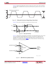
7 series fpgas gtp transceivers user guide www.Xilinx.Com 225 ug482 (v1.9) december 19, 2016 reference clock figure 5-5 illustrates the differential clock input voltage swing, peak-to-peak, which is defined as mgtrefclkp - mgtrefclkn and used in the gtp transceiver portion of the artix-7 fpga data s...
Page 226
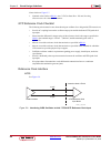
226 www.Xilinx.Com 7 series fpgas gtp transceivers user guide ug482 (v1.9) december 19, 2016 chapter 5: board design guidelines notes relative to figure 5-7 : 1. Nominal values. Refer to ds181 , artix-7 fpgas data sheet: dc and switching characteristics for values and tolerances. Gtp reference clock...
Page 227
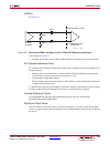
7 series fpgas gtp transceivers user guide www.Xilinx.Com 227 ug482 (v1.9) december 19, 2016 reference clock lvpecl see figure 5-9 . Notes relative to figure 5-9 : 1. Nominal values. Refer to the oscillator vendor data sheet for actual bias resistor requirement. Ac coupled reference clock ac couplin...
Page 228: Power Supply and Filtering
228 www.Xilinx.Com 7 series fpgas gtp transceivers user guide ug482 (v1.9) december 19, 2016 chapter 5: board design guidelines power supply and filtering overview the artix-7 fpga gtp quad requires two analog power supplies: mgtavcc at a nominal voltage level of 1.0 vdc, and mgtavtt at a nominal vo...
Page 229
7 series fpgas gtp transceivers user guide www.Xilinx.Com 229 ug482 (v1.9) december 19, 2016 power supply and filtering there are potentially two major disadvantages to linear regulators; minimum dropout voltage, and limited efficiency. Linear regulators require an input voltage that is higher than ...
Page 230
230 www.Xilinx.Com 7 series fpgas gtp transceivers user guide ug482 (v1.9) december 19, 2016 chapter 5: board design guidelines printed circuit board the decoupling capacitors on the printed circuit board play an important role in minimizing the effects of power supply noise on the transceivers. By ...
Page 231
7 series fpgas gtp transceivers user guide www.Xilinx.Com 231 ug482 (v1.9) december 19, 2016 power supply and filtering another option is to use an 0201 capacitor and mounting it between the vias. An example of this is shown in figure 5-11 . X-ref target - figure 5-10 figure 5-10: placement of 0.1 µ...
Page 232
232 www.Xilinx.Com 7 series fpgas gtp transceivers user guide ug482 (v1.9) december 19, 2016 chapter 5: board design guidelines another choice is to mount an 0201 capacitor next to the bga via pads. Doing this eliminates the need to use filled via in pad. An example of this placement is shown in fig...
Page 233
7 series fpgas gtp transceivers user guide www.Xilinx.Com 233 ug482 (v1.9) december 19, 2016 power supply and filtering table 5-10: csg325 package – 0.1 µf capacitor placement capacitor package pins value mgtavcc mgtavtt gnd cap1 f3 f4 0.1 µf cap2 a2 a1 cap3 b4 b3 cap4 f5 f6 table 5-11: fgg484/fbg48...
Page 234
234 www.Xilinx.Com 7 series fpgas gtp transceivers user guide ug482 (v1.9) december 19, 2016 chapter 5: board design guidelines crosstalk a major contributor to degradation in the performance of an mgt is crosstalk. The mechanisms for crosstalk are aggressor signals coupling into signal traces and/o...
Page 235: Selectio Usage Guidelines
7 series fpgas gtp transceivers user guide www.Xilinx.Com 235 ug482 (v1.9) december 19, 2016 selectio usage guidelines selectio usage guidelines because a gtp transceiver's performance can degrade in an environment flooded with selectio™ activity, it is important to have guidelines for selectio usag...
Page 236
236 www.Xilinx.Com 7 series fpgas gtp transceivers user guide ug482 (v1.9) december 19, 2016 chapter 5: board design guidelines mgttxp0/mgttxn0 mgttxp1/mgttxn1 mgttxp2/mgttxn2 mgttxp3/mgttxn3 • transmitter should be ac coupled to the receiver. The recommended value for the ac coupling capacitors is ...
Page 237
7 series fpgas gtp transceivers user guide www.Xilinx.Com 237 ug482 (v1.9) december 19, 2016 appendix a placement information by package this appendix provides the quad position information for available device and package combinations along with the pad numbers for the external signals associated w...
Page 238
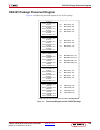
238 www.Xilinx.Com 7 series fpgas gtp transceivers user guide ug482 (v1.9) december 19, 2016 appendix a: placement information by package cpg236 package placement diagram figure a-1 show the placement diagram for the cpg236 package. X-ref target - figure a-1 figure a-1: placement diagram for the cpg...
Page 239
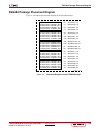
7 series fpgas gtp transceivers user guide www.Xilinx.Com 239 ug482 (v1.9) december 19, 2016 csg325 package placement diagram csg325 package placement diagram figure a-2 and shows the placement diagram for the csg325 package. X-ref target - figure a-2 figure a-2: placement diagram for the csg325 pac...
Page 240
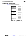
240 www.Xilinx.Com 7 series fpgas gtp transceivers user guide ug482 (v1.9) december 19, 2016 appendix a: placement information by package clg485 package placement diagram figure a-3 and shows the placement diagram for the clg485 package. X-ref target - figure a-3 figure a-3: placement diagram for th...
Page 241
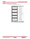
7 series fpgas gtp transceivers user guide www.Xilinx.Com 241 ug482 (v1.9) december 19, 2016 fgg484 package placement diagram fgg484 package placement diagram figure a-4 and shows the placement diagram for the fgg484 package. X-ref target - figure a-4 figure a-4: placement diagram for the fgg484 pac...
Page 242
242 www.Xilinx.Com 7 series fpgas gtp transceivers user guide ug482 (v1.9) december 19, 2016 appendix a: placement information by package fgg676 package placement diagram figure a-5 and figure a-6 show the placement diagram for the fgg676 package. X-ref target - figure a-5 figure a-5: placement diag...
Page 243
7 series fpgas gtp transceivers user guide www.Xilinx.Com 243 ug482 (v1.9) december 19, 2016 fgg676 package placement diagram x-ref target - figure a-6 figure a-6: placement diagram for the fgg676 package (2 of 2) ae7 mgtptxp3_213 af7 mgtptxn3_213 ae11 mgtprxp3_213 af11 mgtprxn3_213 ac8 mgtptxp2_213...
Page 244
244 www.Xilinx.Com 7 series fpgas gtp transceivers user guide ug482 (v1.9) december 19, 2016 appendix a: placement information by package fbg484 package placement diagram figure a-7 show the placement diagram for the fbg484 package. X-ref target - figure a-7 figure a-7: placement diagram for the fbg...
Page 245
7 series fpgas gtp transceivers user guide www.Xilinx.Com 245 ug482 (v1.9) december 19, 2016 sbg484 package placement diagram sbg484 package placement diagram figure a-8 show the placement diagram for the sbg484 package. X-ref target - figure a-8 figure a-8: placement diagram for the sbg484 package ...
Page 246
246 www.Xilinx.Com 7 series fpgas gtp transceivers user guide ug482 (v1.9) december 19, 2016 appendix a: placement information by package fbg676 package placement diagram figure a-9 and figure a-10 show the placement diagram for the fbg676 package. X-ref target - figure a-9 figure a-9: placement dia...
Page 247
7 series fpgas gtp transceivers user guide www.Xilinx.Com 247 ug482 (v1.9) december 19, 2016 fbg676 package placement diagram x-ref target - figure a-10 figure a-10: placement diagram for the fbg676 package (2 of 2) ae7 mgtptxp3_213 af7 mgtptxn3_213 ae11 mgtprxp3_213 af11 mgtprxn3_213 ac8 mgtptxp2_2...
Page 248
248 www.Xilinx.Com 7 series fpgas gtp transceivers user guide ug482 (v1.9) december 19, 2016 appendix a: placement information by package ffg1156 package placement diagram figure a-11 through figure a-14 show the placement diagram for the ffg1156 package. X-ref target - figure a-11 figure a-11: plac...
Page 249
7 series fpgas gtp transceivers user guide www.Xilinx.Com 249 ug482 (v1.9) december 19, 2016 ffg1156 package placement diagram x-ref target - figure a-12 figure a-12: placement diagram for the ffg1156 package (2 of 4) b17 mgtptxp3_116 a17 mgtptxn3_116 f17 mgtprxp3_116 e17 mgtprxn3_116 b15 mgtptxp2_1...
Page 250
250 www.Xilinx.Com 7 series fpgas gtp transceivers user guide ug482 (v1.9) december 19, 2016 appendix a: placement information by package x-ref target - figure a-13 figure a-13: placement diagram for the ffg1156 package (3 of 4) an23 mgtptxp3_213 ap23 mgtptxn3_213 aj21 mgtprxp3_213 ak21 mgtprxn3_213...
Page 251
7 series fpgas gtp transceivers user guide www.Xilinx.Com 251 ug482 (v1.9) december 19, 2016 ffg1156 package placement diagram x-ref target - figure a-14 figure a-14: placement diagram for the ffg1156 package (4 of 4) an13 mgtptxp3_113 ap13 mgtptxn3_113 aj13 mgtprxp3_113 ak13 mgtprxn3_113 al14 mgtpt...
Page 252
252 www.Xilinx.Com 7 series fpgas gtp transceivers user guide ug482 (v1.9) december 19, 2016 appendix a: placement information by package send feedback.
Page 253
7 series fpgas gtp transceivers user guide www.Xilinx.Com 253 ug482 (v1.9) december 19, 2016 appendix b placement information by device table b-1 defines the artix™-7 fpga device-package combinations and the available gtp transceiver banks. Defines the zynq-7000 device-package combinations and the a...
Page 254
254 www.Xilinx.Com 7 series fpgas gtp transceivers user guide ug482 (v1.9) december 19, 2016 appendix b: placement information by device send feedback.
Page 255: 8B/10B Valid Characters
7 series fpgas gtp transceivers user guide www.Xilinx.Com 255 ug482 (v1.9) december 19, 2016 appendix c 8b/10b valid characters 8b/10b encoding includes a set of data characters and k characters. Eight-bit values are coded into 10-bit values, keeping the serial line dc balanced. K characters are spe...
Page 256
256 www.Xilinx.Com 7 series fpgas gtp transceivers user guide ug482 (v1.9) december 19, 2016 appendix c: 8b/10b valid characters d21.0 000 10101 101010 1011 101010 0100 d22.0 000 10110 011010 1011 011010 0100 d23.0 000 10111 111010 0100 000101 1011 d24.0 000 11000 110011 0100 001100 1011 d25.0 000 1...
Page 257
7 series fpgas gtp transceivers user guide www.Xilinx.Com 257 ug482 (v1.9) december 19, 2016 d21.1 001 10101 101010 1001 101010 1001 d22.1 001 10110 011010 1001 011010 1001 d23.1 001 10111 111010 1001 000101 1001 d24.1 001 11000 110011 1001 001100 1001 d25.1 001 11001 100110 1001 100110 1001 d26.1 0...
Page 258
258 www.Xilinx.Com 7 series fpgas gtp transceivers user guide ug482 (v1.9) december 19, 2016 appendix c: 8b/10b valid characters d21.2 010 10101 101010 0101 101010 0101 d22.2 010 10110 011010 0101 011010 0101 d23.2 010 10111 111010 0101 000101 0101 d24.2 010 11000 110011 0101 001100 0101 d25.2 010 1...
Page 259
7 series fpgas gtp transceivers user guide www.Xilinx.Com 259 ug482 (v1.9) december 19, 2016 d21.3 011 10101 101010 1100 101010 0011 d22.3 011 10110 011010 1100 011010 0011 d23.3 011 10111 111010 0011 000101 1100 d24.3 011 11000 110011 0011 001100 1100 d25.3 011 11001 100110 1100 100110 0011 d26.3 0...
Page 260
260 www.Xilinx.Com 7 series fpgas gtp transceivers user guide ug482 (v1.9) december 19, 2016 appendix c: 8b/10b valid characters d21.4 100 10101 101010 1101 101010 0010 d22.4 100 10110 011010 1101 011010 0010 d23.4 100 10111 111010 0010 000101 1101 d24.4 100 11000 110011 0010 001100 1101 d25.4 100 1...
Page 261
7 series fpgas gtp transceivers user guide www.Xilinx.Com 261 ug482 (v1.9) december 19, 2016 d21.5 101 10101 101010 1010 101010 1010 d22.5 101 10110 011010 1010 011010 1010 d23.5 101 10111 111010 1010 000101 1010 d24.5 101 11000 110011 1010 001100 1010 d25.5 101 11001 100110 1010 100110 1010 d26.5 1...
Page 262
262 www.Xilinx.Com 7 series fpgas gtp transceivers user guide ug482 (v1.9) december 19, 2016 appendix c: 8b/10b valid characters d21.6 110 10101 101010 0110 101010 0110 d22.6 110 10110 011010 0110 011010 0110 d23.6 110 10111 111010 0110 000101 0110 d24.6 110 11000 110011 0110 001100 0110 d25.6 110 1...
Page 263
7 series fpgas gtp transceivers user guide www.Xilinx.Com 263 ug482 (v1.9) december 19, 2016 d21.7 111 10101 101010 1110 101010 0001 d22.7 111 10110 011010 1110 011010 0001 d23.7 111 10111 111010 0001 000101 1110 d24.7 111 11000 110011 0001 001100 1110 d25.7 111 11001 100110 1110 100110 0001 d26.7 1...
Page 264
264 www.Xilinx.Com 7 series fpgas gtp transceivers user guide ug482 (v1.9) december 19, 2016 appendix c: 8b/10b valid characters send feedback.
Page 265
7 series fpgas gtp transceivers user guide www.Xilinx.Com 265 ug482 (v1.9) december 19, 2016 appendix d drp address map of the gtp transceiver table d-1 lists the drp map of the gtpe2_common primitive sorted by address. Note: the reserved bits should not be modified. Attributes that are not describe...
Page 266
266 www.Xilinx.Com 7 series fpgas gtp transceivers user guide ug482 (v1.9) december 19, 2016 appendix d: drp address map of the gtp transceiver 001a 15:0 r/w bias_cfg 31:16 0-65535 0-65535 001b 15:0 r/w bias_cfg 47:32 0-65535 0-65535 001c 15:0 r/w bias_cfg 63:48 0-65535 0-65535 0024 15:0 r/w rsvd_at...
Page 267
7 series fpgas gtp transceivers user guide www.Xilinx.Com 267 ug482 (v1.9) december 19, 2016 table d-2 lists the drp map of the gtpe2_channel primitive sorted by address. Note: the reserved bits should not be modified. Attributes that are not described explicitly are set automatically by the 7 serie...
Page 268
268 www.Xilinx.Com 7 series fpgas gtp transceivers user guide ug482 (v1.9) december 19, 2016 appendix d: drp address map of the gtp transceiver 0011 (cont’d) 10:6 r/w rx_clk25_div 4:0 5 4 6 5 7 6 8 7 9 8 10 9 11 10 12 11 13 12 14 13 15 14 16 15 17 16 18 17 19 18 20 19 21 20 22 21 23 22 24 23 25 24 2...
Page 269
7 series fpgas gtp transceivers user guide www.Xilinx.Com 269 ug482 (v1.9) december 19, 2016 0012 9:7 r/w sata_burst_val 2:0 0-7 0-7 0012 6:0 r/w rxoob_cfg 6:0 0-127 0-127 0013 14:9 r/w sas_min_com 5:0 1 1 2 2 3 3 4 4 5 5 6 6 7 7 8 8 9 9 10 10 11 11 12 12 13 13 14 14 15 15 16 16 17 17 18 18 19 19 20...
Page 270
270 www.Xilinx.Com 7 series fpgas gtp transceivers user guide ug482 (v1.9) december 19, 2016 appendix d: drp address map of the gtp transceiver 0013 (cont’d) 14:9 r/w sas_min_com 5:0 31 31 32 32 33 33 34 34 35 35 36 36 37 37 38 38 39 39 40 40 41 41 42 42 43 43 44 44 45 45 46 46 47 47 48 48 49 49 50 ...
Page 271
7 series fpgas gtp transceivers user guide www.Xilinx.Com 271 ug482 (v1.9) december 19, 2016 0013 8:3 r/w sata_min_burst 5:0 1 1 2 2 3 3 4 4 5 5 6 6 7 7 8 8 9 9 10 10 11 11 12 12 13 13 14 14 15 15 16 16 17 17 18 18 19 19 20 20 21 21 22 22 23 23 24 24 25 25 26 26 27 27 28 28 29 29 30 30 31 31 32 32 t...
Page 272
272 www.Xilinx.Com 7 series fpgas gtp transceivers user guide ug482 (v1.9) december 19, 2016 appendix d: drp address map of the gtp transceiver 0013 (cont’d) 8:3 r/w sata_min_burst 5:0 33 33 34 34 35 35 36 36 37 37 38 38 39 39 40 40 41 41 42 42 43 43 44 44 45 45 46 46 47 47 48 48 49 49 50 50 51 51 5...
Page 273
7 series fpgas gtp transceivers user guide www.Xilinx.Com 273 ug482 (v1.9) december 19, 2016 0014 (cont’d) 11:6 r/w sata_min_wake 5:0 3 3 4 4 5 5 6 6 7 7 8 8 9 9 10 10 11 11 12 12 13 13 14 14 15 15 16 16 17 17 18 18 19 19 20 20 21 21 22 22 23 23 24 24 25 25 26 26 27 27 28 28 29 29 30 30 31 31 32 32 ...
Page 274
274 www.Xilinx.Com 7 series fpgas gtp transceivers user guide ug482 (v1.9) december 19, 2016 appendix d: drp address map of the gtp transceiver 0014 (cont’d) 11:6 r/w sata_min_wake 5:0 35 35 36 36 37 37 38 38 39 39 40 40 41 41 42 42 43 43 44 44 45 45 46 46 47 47 48 48 49 49 50 50 51 51 52 52 53 53 5...
Page 275
7 series fpgas gtp transceivers user guide www.Xilinx.Com 275 ug482 (v1.9) december 19, 2016 0014 (cont’d) 5:0 r/w sata_min_init 5:0 4 4 5 5 6 6 7 7 8 8 9 9 10 10 11 11 12 12 13 13 14 14 15 15 16 16 17 17 18 18 19 19 20 20 21 21 22 22 23 23 24 24 25 25 26 26 27 27 28 28 29 29 30 30 31 31 32 32 33 33...
Page 276
276 www.Xilinx.Com 7 series fpgas gtp transceivers user guide ug482 (v1.9) december 19, 2016 appendix d: drp address map of the gtp transceiver 0014 (cont’d) 5:0 r/w sata_min_init 5:0 36 36 37 37 38 38 39 39 40 40 41 41 42 42 43 43 44 44 45 45 46 46 47 47 48 48 49 49 50 50 51 51 52 52 53 53 54 54 55...
Page 277
7 series fpgas gtp transceivers user guide www.Xilinx.Com 277 ug482 (v1.9) december 19, 2016 0015 (cont’d) 12:6 r/w sas_max_com 6:0 5 5 6 6 7 7 8 8 9 9 10 10 11 11 12 12 13 13 14 14 15 15 16 16 17 17 18 18 19 19 20 20 21 21 22 22 23 23 24 24 25 25 26 26 27 27 28 28 29 29 30 30 31 31 32 32 33 33 34 3...
Page 278
278 www.Xilinx.Com 7 series fpgas gtp transceivers user guide ug482 (v1.9) december 19, 2016 appendix d: drp address map of the gtp transceiver 0015 (cont’d) 12:6 r/w sas_max_com 6:0 36 37 37 38 38 39 39 40 40 41 41 42 42 43 43 44 44 45 45 46 46 47 47 48 48 49 49 50 50 51 51 52 52 53 53 54 54 55 55 ...
Page 279
7 series fpgas gtp transceivers user guide www.Xilinx.Com 279 ug482 (v1.9) december 19, 2016 0015 (cont’d) 12:6 r/w sas_max_com 6:0 67 67 68 68 69 69 70 70 71 71 71 71 73 73 74 74 75 75 76 76 77 77 78 78 79 79 80 80 81 81 82 82 83 83 84 84 85 85 86 86 87 87 88 88 89 89 90 90 91 91 92 92 93 93 94 94 ...
Page 280
280 www.Xilinx.Com 7 series fpgas gtp transceivers user guide ug482 (v1.9) december 19, 2016 appendix d: drp address map of the gtp transceiver 0015 (cont’d) 12:6 r/w sas_max_com 6:0 99 99 100 100 101 101 102 102 103 103 104 104 105 105 106 106 107 107 108 108 109 109 110 110 111 111 112 112 113 113...
Page 281
7 series fpgas gtp transceivers user guide www.Xilinx.Com 281 ug482 (v1.9) december 19, 2016 0015 (cont’d) 5:0 r/w sata_max_burst 5:0 4 4 5 5 6 6 7 7 8 8 9 9 10 10 11 11 12 12 13 13 14 14 15 15 16 16 17 17 18 18 19 19 20 20 21 21 22 22 23 23 24 24 25 25 26 26 27 27 28 28 29 29 30 30 31 31 32 32 33 3...
Page 282
282 www.Xilinx.Com 7 series fpgas gtp transceivers user guide ug482 (v1.9) december 19, 2016 appendix d: drp address map of the gtp transceiver 0015 (cont’d) 5:0 r/w sata_max_burst 5:0 36 36 37 37 38 38 39 39 40 40 41 41 42 42 43 43 44 44 45 45 46 46 47 47 48 48 49 49 50 50 51 51 52 52 53 53 54 54 5...
Page 283
7 series fpgas gtp transceivers user guide www.Xilinx.Com 283 ug482 (v1.9) december 19, 2016 0016 (cont’d) 11:6 r/w sata_max_wake 5:0 5 5 6 6 7 7 8 8 9 9 10 10 11 11 12 12 13 13 14 14 15 15 16 16 17 17 18 18 19 19 20 20 21 21 22 22 23 23 24 24 25 25 26 26 27 27 28 28 29 29 30 30 31 31 32 32 33 33 34...
Page 284
284 www.Xilinx.Com 7 series fpgas gtp transceivers user guide ug482 (v1.9) december 19, 2016 appendix d: drp address map of the gtp transceiver 0016 (cont’d) 11:6 r/w sata_max_wake 5:0 37 37 38 38 39 39 40 40 41 41 42 42 43 43 44 44 45 45 46 46 47 47 48 48 49 49 50 50 51 51 52 52 53 53 54 54 55 55 5...
Page 285
7 series fpgas gtp transceivers user guide www.Xilinx.Com 285 ug482 (v1.9) december 19, 2016 0016 (cont’d) 5:0 r/w sata_max_init 5:0 6 6 7 7 8 8 9 9 10 10 11 11 12 12 13 13 14 14 15 15 16 16 17 17 18 18 19 19 20 20 21 21 22 22 23 23 24 24 25 25 26 26 27 27 28 28 29 29 30 30 31 31 32 32 33 33 34 34 3...
Page 286
286 www.Xilinx.Com 7 series fpgas gtp transceivers user guide ug482 (v1.9) december 19, 2016 appendix d: drp address map of the gtp transceiver 0016 (cont’d) 5:0 r/w sata_max_init 5:0 38 38 39 39 40 40 41 41 42 42 43 43 44 44 45 45 46 46 47 47 48 48 49 49 50 50 51 51 52 52 53 53 54 54 55 55 56 56 57...
Page 287
7 series fpgas gtp transceivers user guide www.Xilinx.Com 287 ug482 (v1.9) december 19, 2016 0019 8:6 r/w tx_eidle_assert_delay 2:0 0-7 0-7 0019 5 r/w tx_loopback_drive_hiz 0 false 0 true 1 0019 4:0 r/w tx_drive_mode 0 direct 0 pipe 1 001a 15:8 r/w pd_trans_time_to_p2 7:0 0-255 0-255 001a 7:0 r/w pd...
Page 288
288 www.Xilinx.Com 7 series fpgas gtp transceivers user guide ug482 (v1.9) december 19, 2016 appendix d: drp address map of the gtp transceiver 0036 15:0 r/w es_sdata_mask 15:0 0-65535 0-65535 0037 15:0 r/w es_sdata_mask 31:16 0-65535 0-65535 0038 15:0 r/w es_sdata_mask 47:32 0-65535 0-65535 0039 15...
Page 289
7 series fpgas gtp transceivers user guide www.Xilinx.Com 289 ug482 (v1.9) december 19, 2016 0041 (cont’d) 12:8 r/w rx_sig_valid_dly 4:0 3 2 4 3 5 4 6 5 7 6 8 7 9 8 10 9 11 10 12 11 13 12 14 13 15 14 16 15 17 16 18 17 19 18 20 19 21 20 22 21 23 22 24 23 25 24 26 25 27 26 28 27 29 28 30 29 31 30 32 3...
Page 290
290 www.Xilinx.Com 7 series fpgas gtp transceivers user guide ug482 (v1.9) december 19, 2016 appendix d: drp address map of the gtp transceiver 0041 6 r/w align_mcomma_det 0 false 0 true 1 0041 5 r/w show_realign_comma 0 false 0 true 1 0041 4 r/w align_comma_double 0 false 0 true 1 0041 3:0 r/w rxsl...
Page 291
7 series fpgas gtp transceivers user guide www.Xilinx.Com 291 ug482 (v1.9) december 19, 2016 0045 (cont’d) 15:10 r/w clk_cor_max_lat 5:0 9 9 10 10 11 11 12 12 13 13 14 14 15 15 16 16 17 17 18 18 19 19 20 20 21 21 22 22 23 23 24 24 25 25 26 26 27 27 28 28 29 29 30 30 31 31 32 32 33 33 34 34 35 35 36 ...
Page 292
292 www.Xilinx.Com 7 series fpgas gtp transceivers user guide ug482 (v1.9) december 19, 2016 appendix d: drp address map of the gtp transceiver 0045 (cont’d) 15:10 r/w clk_cor_max_lat 5:0 40 40 41 41 42 42 43 43 44 44 45 45 46 46 47 47 48 48 49 49 50 50 51 51 52 52 53 53 54 54 55 55 56 56 57 57 58 5...
Page 293
7 series fpgas gtp transceivers user guide www.Xilinx.Com 293 ug482 (v1.9) december 19, 2016 0046 (cont’d) 15:10 r/w clk_cor_min_lat 5:0 13 13 14 14 15 15 16 16 17 17 18 18 19 19 20 20 21 21 22 22 23 23 24 24 25 25 26 26 27 27 28 28 29 29 30 30 31 31 32 32 33 33 34 34 35 35 36 36 37 37 38 38 39 39 4...
Page 294
294 www.Xilinx.Com 7 series fpgas gtp transceivers user guide ug482 (v1.9) december 19, 2016 appendix d: drp address map of the gtp transceiver 0046 (cont’d) 15:10 r/w clk_cor_min_lat 5:0 45 45 46 46 47 47 48 48 49 49 50 50 51 51 52 52 53 53 54 54 55 55 56 56 57 57 58 58 59 59 60 60 0046 9:0 r/w clk...
Page 295
7 series fpgas gtp transceivers user guide www.Xilinx.Com 295 ug482 (v1.9) december 19, 2016 0047 (cont’d) 14:10 r/w clk_cor_repeat_wait 4:0 15 15 16 16 17 17 18 18 19 19 20 20 21 21 22 22 23 23 24 24 25 25 26 26 27 27 28 28 29 29 30 30 31 31 0047 9:0 r/w clk_cor_seq_1_4 9:0 0-1023 0-1023 0048 14 r/...
Page 296
296 www.Xilinx.Com 7 series fpgas gtp transceivers user guide ug482 (v1.9) december 19, 2016 appendix d: drp address map of the gtp transceiver 004b 15 r/w rxgearbox_en 0 false 0 true 1 004b 9:0 r/w clk_cor_seq_2_4 9:0 0-1023 0-1023 004c 15:12 r/w chan_bond_seq_1_enable 3:0 0-15 0-15 004c 9:0 r/w ch...
Page 297
7 series fpgas gtp transceivers user guide www.Xilinx.Com 297 ug482 (v1.9) december 19, 2016 0053 (cont’d) 15:12 r/w chan_bond_max_skew 3:0 7 7 8 8 9 9 10 10 11 11 12 12 13 13 14 14 0053 9:0 r/w chan_bond_seq_2_4 9:0 0-1023 0-1023 0054 15:0 r/w rxdly_tap_cfg 15:0 0-65535 0-65535 0055 15:0 r/w rxdly_...
Page 298
298 www.Xilinx.Com 7 series fpgas gtp transceivers user guide ug482 (v1.9) december 19, 2016 appendix d: drp address map of the gtp transceiver 0064 15:0 r/w txph_cfg 15:0 0-65535 0-65535 0065 12:8 r/w txph_monitor_sel 4:0 0-31 0-31 0066 15:0 r/w rx_bias_cfg 15:0 0-65535 0-65535 0068 3 r/w rxoob_clk...
Page 299
7 series fpgas gtp transceivers user guide www.Xilinx.Com 299 ug482 (v1.9) december 19, 2016 006a (cont’d) 4:0 r/w tx_clk25_div 4:0 24 23 25 24 26 25 27 26 28 27 29 28 30 29 31 30 32 31 006b 15 r/w pma_rsv5 0 0-1 0-1 006b 11:8 r/w pma_rsv4 3:0 0-15 0-15 006b 2:0 r/w tx_data_width 2:0 16 2 20 3 32 4 ...
Page 300
300 www.Xilinx.Com 7 series fpgas gtp transceivers user guide ug482 (v1.9) december 19, 2016 appendix d: drp address map of the gtp transceiver 007c 1:0 r/w pma_rsv3 1:0 0-3 0-3 007d 15 r/w pma_rsv7 0 0-1 0-1 007d 14 r/w pma_rsv6 0 0-1 0-1 007d 13:0 r/w tx_rxdetect_cfg 13:0 0-16383 0-16383 007e 15 r...
Page 301
7 series fpgas gtp transceivers user guide www.Xilinx.Com 301 ug482 (v1.9) december 19, 2016 008e 14 r/w rxlpm_incm_cfg 0 0-1 0-1 008e 13 r/w cfok_cfg4 0 0-1 0-1 008e 12:9 r/w cfok_cfg6 3:0 0-15 0-15 008e 8:0 r/w rxlpm_gc_cfg 8:0 0-511 0-511 008f 7:5 r/w rxlpm_gc_cfg2 2:0 0-7 0-7 008f 4 r/w rxpi_cfg...
Page 302
302 www.Xilinx.Com 7 series fpgas gtp transceivers user guide ug482 (v1.9) december 19, 2016 appendix d: drp address map of the gtp transceiver 009c (cont’d) 5:0 r/w rxbuf_thresh_undflw 5:0 4 4 5 5 6 6 7 7 8 8 9 9 10 10 11 11 12 12 13 13 14 14 15 15 16 16 17 17 18 18 19 19 20 20 21 21 22 22 23 23 24...
Page 303
7 series fpgas gtp transceivers user guide www.Xilinx.Com 303 ug482 (v1.9) december 19, 2016 009c (cont’d) 5:0 r/w rxbuf_thresh_undflw 5:0 36 36 37 37 38 38 39 39 40 40 41 41 42 42 43 43 44 44 45 45 46 46 47 47 48 48 49 49 50 50 51 51 52 52 53 53 54 54 55 55 56 56 57 57 58 58 59 59 60 60 61 61 62 62...
Page 304
304 www.Xilinx.Com 7 series fpgas gtp transceivers user guide ug482 (v1.9) december 19, 2016 appendix d: drp address map of the gtp transceiver 009d 6:1 r/w rxbuf_thresh_ovflw 5:0 0 0 1 1 2 2 3 3 4 4 5 5 6 6 7 7 8 8 9 9 10 10 11 11 12 12 13 13 14 14 15 15 16 16 17 17 18 18 19 19 20 20 21 21 22 22 23...
Page 305
7 series fpgas gtp transceivers user guide www.Xilinx.Com 305 ug482 (v1.9) december 19, 2016 009d (cont’d) 6:1 r/w rxbuf_thresh_ovflw 5:0 32 32 33 33 34 34 35 35 36 36 37 37 38 38 39 39 40 40 41 41 42 42 43 43 44 44 45 45 46 46 47 47 48 48 49 49 50 50 51 51 52 52 53 53 54 54 55 55 56 56 57 57 58 58 ...
Page 306
306 www.Xilinx.Com 7 series fpgas gtp transceivers user guide ug482 (v1.9) december 19, 2016 appendix d: drp address map of the gtp transceiver 009d 0 r/w rx_defer_reset_buf_en 0 false 0 true 1 009e 2 r/w rxbuf_reset_on_commaalign 0 false 0 true 1 009e 1 r/w rxbuf_reset_on_rate_change 0 false 0 true...


