- DL manuals
- Xilinx
- Motherboard
- AC701
- User Manual
Xilinx AC701 User Manual
Summary of AC701
Page 1
Ac701 evaluation board for the artix-7 fpga user guide ug952 (v1.3) april 7, 2015.
Page 2: Revision History
Ac701 evaluation board www.Xilinx.Com ug952 (v1.3) april 7, 2015 disclaimer the information disclosed to you hereunder (the “materials”) is provided solely for the selection and use of xilinx products. To the maximum extent permitted by applicable law: (1) materials are made available "as is" and wi...
Page 3
Ug952 (v1.3) april 7, 2015 www.Xilinx.Com ac701 evaluation board 04/07/2015 1.3 replaced the board photo in figure 1-2 with the rev 2.0 board. Added callout row to gtp transceiver clock multiplexers in table 1-1 . Replaced table 1-4 , table 1-5 , table 1-7 , and table 1-8 . Replaced i/o banks 32, 33...
Page 4
Ac701 evaluation board www.Xilinx.Com ug952 (v1.3) april 7, 2015.
Page 5: Table of Contents
Ac701 evaluation board www.Xilinx.Com 5 ug952 (v1.3) april 7, 2015 revision history . . . . . . . . . . . . . . . . . . . . . . . . . . . . . . . . . . . . . . . . . . . . . . . . . . . . . . . . . . . . . 2 chapter 1: ac701 evaluation board features overview . . . . . . . . . . . . . . . . . . . . ...
Page 6
6 www.Xilinx.Com ac701 evaluation board ug952 (v1.3) april 7, 2015 appendix d: board setup installing the ac701 board in a pc chassis . . . . . . . . . . . . . . . . . . . . . . . . . . . . . . . . . 101 appendix e: board specifications dimensions . . . . . . . . . . . . . . . . . . . . . . . . . . ...
Page 7: Overview
Ac701 evaluation board www.Xilinx.Com 7 ug952 (v1.3) april 7, 2015 chapter 1 ac701 evaluation board features overview the ac701 evaluation board for the artix®-7 fpga provides a hardware environment for developing and evaluating designs targeting the artix-7 xc7a200t-2fbg676c fpga. The ac701 board p...
Page 8
8 www.Xilinx.Com ac701 evaluation board ug952 (v1.3) april 7, 2015 chapter 1: ac701 evaluation board features • gen1 4-lane (x4) • gen2 4-lane (x4) • sfp+ connector • 10/100/1,000 tri-speed ethernet phy • usb-to-uart bridge • high-definition multimedia interface (hdmi™) technology codec • i2c bus • ...
Page 9
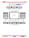
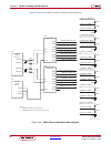
Ac701 evaluation board www.Xilinx.Com 9 ug952 (v1.3) april 7, 2015 overview the ac701 board block diagram is shown in figure 1-1 . The ac701 board schematics are available for download from the ac701 evaluation kit product page. Caution! The ac701 board can be damaged by electrostatic discharge (esd...
Page 10: Feature Descriptions
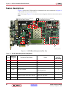
10 www.Xilinx.Com ac701 evaluation board ug952 (v1.3) april 7, 2015 chapter 1: ac701 evaluation board features feature descriptions figure 1-2 shows the ac701 board. Each numbered feature that is referenced in figure 1-2 is described in the sections that follow. Note: the image in figure 1-2 is for ...
Page 11
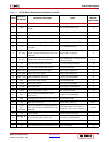
Ac701 evaluation board www.Xilinx.Com 11 ug952 (v1.3) april 7, 2015 feature descriptions 9 j25, j26 sma gtp reference clock input rosenberger 32k10k-400l5 3 10 u24 jitter attenuated clock (back side of board) silicon labs si5324-c-gm 16 11 u1 gtp transceivers embedded within fpga u1 30 12 p1 pci exp...
Page 12
12 www.Xilinx.Com ac701 evaluation board ug952 (v1.3) april 7, 2015 chapter 1: ac701 evaluation board features artix-7 fpga [ figure 1-2 , callout 1 ] the ac701 board is populated with the artix-7 xc7a200t-2fbg676c fpga. For further information on artix-7 fpgas, see 7 series fpgas overview (ds180) [...
Page 13
Ac701 evaluation board www.Xilinx.Com 13 ug952 (v1.3) april 7, 2015 feature descriptions for full details on configuring the fpga, see 7 series fpgas configuration user guide (ug470) [ref 5] . Encryption key backup circuit fpga u1 implements bitstream encryption key technology. The ac701 board provi...
Page 14
14 www.Xilinx.Com ac701 evaluation board ug952 (v1.3) april 7, 2015 chapter 1: ac701 evaluation board features ddr3 memory module [ figure 1-2 , callout 2 ] the memory module at j1 is a 1 gb ddr3 small outline dual-inline memory module (sodimm). It provides volatile synchronous dynamic random access...
Page 15
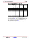
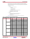
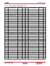
Ac701 evaluation board www.Xilinx.Com 15 ug952 (v1.3) april 7, 2015 feature descriptions k2 ddr3_a15 sstl15 78 a15 n1 ddr3_ba0 sstl15 109 ba0 m1 ddr3_ba1 sstl15 108 ba1 h2 ddr3_ba2 sstl15 79 ba2 ab6 ddr3_d0 sstl15 5 dq0 aa8 ddr3_d1 sstl15 7 dq1 y8 ddr3_d2 sstl15 15 dq2 ab5 ddr3_d3 sstl15 17 dq3 aa5 ...
Page 16
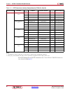
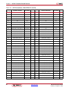
16 www.Xilinx.Com ac701 evaluation board ug952 (v1.3) april 7, 2015 chapter 1: ac701 evaluation board features w4 ddr3_d28 sstl15 56 dq28 w5 ddr3_d29 sstl15 58 dq29 w1 ddr3_d30 sstl15 68 dq30 v1 ddr3_d31 sstl15 70 dq31 g2 ddr3_d32 sstl15 129 dq32 d1 ddr3_d33 sstl15 131 dq33 e1 ddr3_d34 sstl15 141 dq...
Page 17
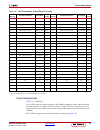
Ac701 evaluation board www.Xilinx.Com 17 ug952 (v1.3) april 7, 2015 feature descriptions g8 ddr3_d60 sstl15 180 dq60 h8 ddr3_d61 sstl15 182 dq61 d6 ddr3_d62 sstl15 192 dq62 e6 ddr3_d63 sstl15 194 dq63 ac6 ddr3_dm0 sstl15 11 dm0 ac4 ddr3_dm1 sstl15 28 dm1 aa3 ddr3_dm2 sstl15 46 dm2 u7 ddr3_dm3 sstl15...
Page 18
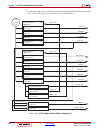
18 www.Xilinx.Com ac701 evaluation board ug952 (v1.3) april 7, 2015 chapter 1: ac701 evaluation board features the ac701 board ddr3 memory interface adheres to the constraints guidelines documented in the ddr3 design guidelines section of the 7 series fpgas memory interface solutions user guide (ug5...
Page 19
Ac701 evaluation board www.Xilinx.Com 19 ug952 (v1.3) april 7, 2015 feature descriptions quad spi flash memory [ figure 1-2 , callout 3 ] the quad spi flash memory u7 provides 256 mb of nonvolatile storage that can be used for configuration and data storage. • part number: n25q256a13esf40g (micron) ...
Page 20
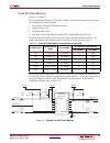
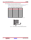
20 www.Xilinx.Com ac701 evaluation board ug952 (v1.3) april 7, 2015 chapter 1: ac701 evaluation board features spi flash memory external programming header in addition to the quad spi device fpga u1 connections shown in table 1-5 , the fpga u1 spi flash memory interface is connected to an external p...
Page 21
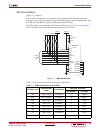
Ac701 evaluation board www.Xilinx.Com 21 ug952 (v1.3) april 7, 2015 feature descriptions sd card interface [ figure 1-2 , callout 4 ] the ac701 board includes a secure digital input/output (sdio) interface to provide user-logic access to general purpose nonvolatile sdio memory cards and peripherals....
Page 22
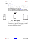
22 www.Xilinx.Com ac701 evaluation board ug952 (v1.3) april 7, 2015 chapter 1: ac701 evaluation board features usb jtag module [ figure 1-2 , callout 5 ] jtag configuration is provided through a digilent onboard usb-to-jtag configuration logic module (u26) where a host computer accesses the ac701 bo...
Page 23
Ac701 evaluation board www.Xilinx.Com 23 ug952 (v1.3) april 7, 2015 feature descriptions the jtag connectivity on the ac701 board allows a host computer to download bitstreams to the fpga using xilinx software tools. In addition, the jtag connector allows debug tools or a software debugger to access...
Page 24
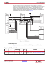
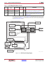
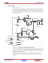
24 www.Xilinx.Com ac701 evaluation board ug952 (v1.3) april 7, 2015 chapter 1: ac701 evaluation board features the ac701 clocking diagram is shown in figure 1-10 . The fpga logic clock source circuits are detailed first after figure 1-10 , followed by the gtp clock sources circuitry descriptions in ...
Page 25
Ac701 evaluation board www.Xilinx.Com 25 ug952 (v1.3) april 7, 2015 feature descriptions system clock source [ figure 1-2 , callout 6 ] the ac701 board has a 2.5v lvds differential 200 mhz oscillator (u51) soldered onto the back side of the board and wired to an fpga mrcc clock input on bank 34. Thi...
Page 26
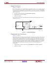
26 www.Xilinx.Com ac701 evaluation board ug952 (v1.3) april 7, 2015 chapter 1: ac701 evaluation board features the user clock circuit is shown in figure 1-12 . The silicon labs si570 data sheet is available from their website [ref 21] . User sma clock input [ figure 1-2 , callout 8 ] an external hig...
Page 27
Ac701 evaluation board www.Xilinx.Com 27 ug952 (v1.3) april 7, 2015 feature descriptions gtp transceiver clock multiplexer [ figure 1-2 , callout 35 ] the ac701 board provides flexible gtp quad 213 mgtrefclk options through the use of external multiplexer (mux) components u3 and u4 to service the gt...
Page 28
28 www.Xilinx.Com ac701 evaluation board ug952 (v1.3) april 7, 2015 chapter 1: ac701 evaluation board features clock multiplexer u3 sy89544umg drives bank 213 mgtrefclk0 pins aa13 (p) and ab13 (n). See table 1-10 for clock mux u3 connections. The multiplexer u3 clock input channel select nets are sf...
Page 29
Ac701 evaluation board www.Xilinx.Com 29 ug952 (v1.3) april 7, 2015 feature descriptions x-ref target - figure 1-15 figure 1-15: mgt clock multiplexer u3 circuit q24 nd s33 6p 460 mw s fp_mgt_clk_ s el0 mgt_clk0_ s el0 mgt_clk0_ s el1 s fp_mgt_clk0_p s fp_mgt_clk0_p 0 vcc1 vcc2 fmc1_hbc_gbtclk0_m2c_...
Page 30
30 www.Xilinx.Com ac701 evaluation board ug952 (v1.3) april 7, 2015 chapter 1: ac701 evaluation board features clock multiplexer u4 sy89544umg drives bank 213 mgtrefclk1 pins aa11 (p) and ab11(n). See table 1-11 for clock multiplexer u4 connections. The multiplexer u4 clock input channel select nets...
Page 31
Ac701 evaluation board www.Xilinx.Com 31 ug952 (v1.3) april 7, 2015 feature descriptions x-ref target - figure 1-16 figure 1-16: mgt clock multiplexer u4 circuit q2 3 nd s33 6p 460 mw pcie_mgt_clk_ s el0 mgt_clk1_ s el0 mgt_clk1_ s el1 s fp_mgt_clk1_p s fp_mgt_clk1_p 0 vcc1 vcc2 fmc1_hbc_gbtclk1_m2c...
Page 32
32 www.Xilinx.Com ac701 evaluation board ug952 (v1.3) april 7, 2015 chapter 1: ac701 evaluation board features gtp transceiver clock multiplexer input clock sources this section describes the gtp 213 multiplexer u3 and u4 input clock circuits as listed in table 1-11 . U3 in0: 125 mhz clock generator...
Page 33
Ac701 evaluation board www.Xilinx.Com 33 ug952 (v1.3) april 7, 2015 feature descriptions u3/u4 in1: jitter attenuated clock [ figure 1-2 , callout 10 ] the ac701 board includes a silicon labs si5324 jitter attenuator u24 on the back side of the board. Fpga user logic can implement a clock recovery c...
Page 34
34 www.Xilinx.Com ac701 evaluation board ug952 (v1.3) april 7, 2015 chapter 1: ac701 evaluation board features u4 in0: gtp transceiver sma clock input [ figure 1-2 , callout 9 ] the ac701 board includes a pair of sma connectors for a gtp transceiver clock that are wired to gtp quad bank 213 through ...
Page 35
Ac701 evaluation board www.Xilinx.Com 35 ug952 (v1.3) april 7, 2015 feature descriptions the gtp transceivers in 7 series fpgas are grouped into four channels described as quads. The reference clock for a quad can be sourced from the quad above or quad below the gtp quad of interest. There are two g...
Page 36
36 www.Xilinx.Com ac701 evaluation board ug952 (v1.3) april 7, 2015 chapter 1: ac701 evaluation board features for more information on the gtp transceivers see 7 series fpgas gtx/gth transceivers user guide (ug476) [ref 7] . Gtp_bank_216 gtpe2_channel_ x0y4 b7 mgtptxp0_216 pcie_tx3_p p1.A29 (2) pcie...
Page 37
Ac701 evaluation board www.Xilinx.Com 37 ug952 (v1.3) april 7, 2015 feature descriptions pci express edge connector [ figure 1-2 , callout 12 ] the 4-lane pci express edge connector performs data transfers at the rate of 2.5 gt/s for a gen1 application and 5.0 gt/s for a gen2 application. The pcie t...
Page 38
38 www.Xilinx.Com ac701 evaluation board ug952 (v1.3) april 7, 2015 chapter 1: ac701 evaluation board features sfp/sfp+ connector [ figure 1-2 , callout 13 ] the ac701 board contains a small form-factor pluggable (sfp+) connector and cage assembly (p3) that accepts sfp or sfp+ modules. Figure 1-22 s...
Page 39
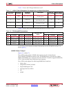
Ac701 evaluation board www.Xilinx.Com 39 ug952 (v1.3) april 7, 2015 feature descriptions table 1-13 lists the sfp+ module receive and transmit connections to the fpga. Table 1-14 lists the sfp+ module control and status connections. Table 1-13: fpga u1 to sfp+ module connections fpga pin (u1) schema...
Page 40
40 www.Xilinx.Com ac701 evaluation board ug952 (v1.3) april 7, 2015 chapter 1: ac701 evaluation board features 10/100/1000 mb/s tri-speed ethernet phy [ figure 1-2 , callout 14 ] the ac701 board uses the marvell alaska phy device (88e1116r) at u12 for ethernet communications at 10 mb/s, 100 mb/s, or...
Page 41
Ac701 evaluation board www.Xilinx.Com 41 ug952 (v1.3) april 7, 2015 feature descriptions the ethernet connections from the xc7a200t at u1 to the 88e1116r phy device at u12 are listed in table 1-16 ethernet phy connections to fpga u1. Ethernet phy clock source a 25.00 mhz, 50 ppm crystal at x1 is the...
Page 42
42 www.Xilinx.Com ac701 evaluation board ug952 (v1.3) april 7, 2015 chapter 1: ac701 evaluation board features ethernet phy user leds [ figure 1-2 , callout 20 ] the three ethernet phy user leds shown in figure 1-24 are located near the rj45 ethernet jack p4. The on/off state for each led is softwar...
Page 43
Ac701 evaluation board www.Xilinx.Com 43 ug952 (v1.3) april 7, 2015 feature descriptions table 1-17 shows the usb signal definitions at j17. Table 1-18 shows the usb connections between the fpga and the uart. See the silicon labs website for technical information on the cp2103gm and the vcp drivers ...
Page 44
44 www.Xilinx.Com ac701 evaluation board ug952 (v1.3) april 7, 2015 chapter 1: ac701 evaluation board features figure 1-25 shows the hdmi codec circuit. X-ref target - figure 1-25 figure 1-25: hdmi codec circuit ug952_c1_2 3 _100 3 12 gnd gnd vcc 3 v 3 gnd gnd oe gnd out vcc d 3 1 d 3 2 d 33 d 3 4 d...
Page 45
Ac701 evaluation board www.Xilinx.Com 45 ug952 (v1.3) april 7, 2015 feature descriptions table 1-19 lists the connections between the codec and the fpga. Table 1-19: fpga to hdmi codec connections (adv7511) fpga pin (u1) schematic net name i/o standard adv7511 (u48) pin pin name aa24 hdmi_r_d4 lvcmo...
Page 46
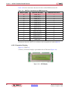
46 www.Xilinx.Com ac701 evaluation board ug952 (v1.3) april 7, 2015 chapter 1: ac701 evaluation board features table 1-20 lists the connections between the codec and the hdmi connector p2. Information about the adv7511 is available on the analog devices website [ref 16] . Lcd character display [ fig...
Page 47
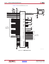
Ac701 evaluation board www.Xilinx.Com 47 ug952 (v1.3) april 7, 2015 feature descriptions the character display runs at 5.0v and is connected to the fpga 3.3v hp bank 14 through a ti txs0108e 8-bit bidirectional voltage level translator (u45). Figure 1-27 shows the lcd interface circuit. The ac701 bo...
Page 48
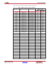
48 www.Xilinx.Com ac701 evaluation board ug952 (v1.3) april 7, 2015 chapter 1: ac701 evaluation board features table 1-21 lists the connections between the fpga and the lcd header. If the lcd is not installed, the j23 pins listed in table 1-21 can be used for gpio. For the displaytech s162dbabc lcd ...
Page 49
Ac701 evaluation board www.Xilinx.Com 49 ug952 (v1.3) april 7, 2015 feature descriptions table 1-22 lists the address for each bus. Information about the pca9548 is available on the ti semiconductor website [ref 22] . Ac701 board leds table 1-23 lists all leds on the ac701 board. Table 1-22: i2c bus...
Page 50
50 www.Xilinx.Com ac701 evaluation board ug952 (v1.3) april 7, 2015 chapter 1: ac701 evaluation board features user i/o [ figure 1-2 , callout 21 – 25 ] the ac701 board provides the following user and general purpose i/o capabilities: • four user gpio leds (callout 21 ) • gpio_led_[3-0]: ds5, ds4, d...
Page 51
Ac701 evaluation board www.Xilinx.Com 51 ug952 (v1.3) april 7, 2015 feature descriptions user gpio leds [ figure 1-2 , callout 21 ] figure 1-30 shows the user led circuits. User pushbuttons and reset switch [ figure 1-2 , callout 22 ] figure 1-31 shows the user pushbutton switch circuits. X-ref targ...
Page 52
52 www.Xilinx.Com ac701 evaluation board ug952 (v1.3) april 7, 2015 chapter 1: ac701 evaluation board features figure 1-32 shows the user cpu_reset pushbutton switch circuit. Gpio dip switch [ figure 1-2 , callout 23 ] figure 1-33 shows the gpio dip switch circuit. User rotary switch [ figure 1-2 , ...
Page 53
Ac701 evaluation board www.Xilinx.Com 53 ug952 (v1.3) april 7, 2015 feature descriptions user sma connectors [ figure 1-2 , callout 25 ] figure 1-35 shows the user sma connector circuit. Lcd connector figure 1-36 shows the lcd j23 2x7 male pin header circuit. Pmod connector figure 1-37 shows the j48...
Page 54
54 www.Xilinx.Com ac701 evaluation board ug952 (v1.3) april 7, 2015 chapter 1: ac701 evaluation board features table 1-24 lists the gpio connections to fpga u1. Table 1-24: gpio connections to fpga u1 fpga pin (u1) schematic net name i/o standard gpio component pin user leds (active high) m26 gpio_l...
Page 55
Ac701 evaluation board www.Xilinx.Com 55 ug952 (v1.3) april 7, 2015 feature descriptions switches [ figure 1-2 , callout 26 – 27 ] the ac701 board includes a power and a configuration switch: • power on/off slide switch sw15 (callout 26 ) • fpga_program_b sw14, active-low (callout 27 ) power on/off ...
Page 56
56 www.Xilinx.Com ac701 evaluation board ug952 (v1.3) april 7, 2015 chapter 1: ac701 evaluation board features fpga_prog_b pushbutton sw9 (active-low) [ figure 1-2 , callout 27 ] switch sw9 grounds the fpga program_b pin when pressed. This action initiates an fpga reconfiguration. The fpga_prog_b si...
Page 57
Ac701 evaluation board www.Xilinx.Com 57 ug952 (v1.3) april 7, 2015 feature descriptions the default mode setting is m[2:0] = 001 , which selects master spi flash memory at board power-on. See 7 series fpgas configuration user guide (ug470) [ref 5] for further details on configuring the 7 series fpg...
Page 58
58 www.Xilinx.Com ac701 evaluation board ug952 (v1.3) april 7, 2015 chapter 1: ac701 evaluation board features • 4 gtp transceivers • 2 gtp transceiver clocks • 2 differential clocks • 159 ground and 15 power connections note: the ac701 board vadj voltage for hpc connector j30 is determined by the f...
Page 59
Ac701 evaluation board www.Xilinx.Com 59 ug952 (v1.3) april 7, 2015 feature descriptions c22 fmc1_hpc_la18_cc_p lvcmos25 g20 d18 fmc1_hpc_la13_n lvcmos25 a20 c23 fmc1_hpc_la18_cc_n lvcmos25 g21 d20 fmc1_hpc_la17_cc_p lvcmos25 k21 c26 fmc1_hpc_la27_p lvcmos25 f23 d21 fmc1_hpc_la17_cc_n lvcmos25 j21 c...
Page 60
60 www.Xilinx.Com ac701 evaluation board ug952 (v1.3) april 7, 2015 chapter 1: ac701 evaluation board features e30 nc na na f29 nc na na e31 nc na na f31 nc na na e33 nc na na f32 nc na na e34 nc na na f34 nc na na e36 nc na na f35 nc na na e37 nc na na f37 nc na na e39 vcco_vadj na na f38 nc na na ...
Page 61
Ac701 evaluation board www.Xilinx.Com 61 ug952 (v1.3) april 7, 2015 feature descriptions power management [ figure 1-2 , callout 30 ] the ac701 board uses power regulators and pmbus compliant system controllers from texas instruments to supply core and auxiliary voltages. The texas instruments fusio...
Page 62
62 www.Xilinx.Com ac701 evaluation board ug952 (v1.3) april 7, 2015 chapter 1: ac701 evaluation board features the pcb layout and power system design meets the recommended criteria described in the 7 series fpgas pcb design and pin planning guide (ug483) [ref 11] . X-ref target - figure 1-42 figure ...
Page 63
Ac701 evaluation board www.Xilinx.Com 63 ug952 (v1.3) april 7, 2015 feature descriptions the ac701 board core and auxiliary voltages are listed in table 1-27 . Table 1-27: ac701 board onboard power system devices device type reference designator description power rail net name power rail voltage sch...
Page 64
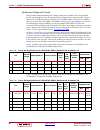
64 www.Xilinx.Com ac701 evaluation board ug952 (v1.3) april 7, 2015 chapter 1: ac701 evaluation board features monitoring voltage and current voltage and current monitoring and voltage control are available for the ti controlled power rails through the texas instruments fusion digital power designer...
Page 65
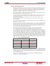
Ac701 evaluation board www.Xilinx.Com 65 ug952 (v1.3) april 7, 2015 feature descriptions vcco_vadj voltage control the fmc vcco_vadj rail is set to 2.5v. When the ac701 board is powered on, the state of the fmc_vadj_on_b signal wired to header j8 is sampled by the ti ucd90120a controller u9. If a ju...
Page 66
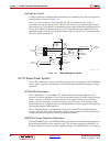
66 www.Xilinx.Com ac701 evaluation board ug952 (v1.3) april 7, 2015 chapter 1: ac701 evaluation board features cooling fan control cooling fan rpm is controlled and monitored by user-created ip in the fpga using the fan control circuit is shown in figure 1-43 . Fpga u1 can be cooled by a user-suppli...
Page 67
Ac701 evaluation board www.Xilinx.Com 67 ug952 (v1.3) april 7, 2015 feature descriptions input voltage rail between 4.5v and 14.5v and deliver an adjustable output voltage in the 0.6v to 5.5v range. This type of power solution allows as few as three external components and eliminates the loop compen...
Page 68
68 www.Xilinx.Com ac701 evaluation board ug952 (v1.3) april 7, 2015 chapter 1: ac701 evaluation board features figure 1-44 shows the power system for ucd90120a u8 controller #1 x-ref target - figure 1-44 figure 1-44: u8 controller #1 ucd90120a power system ug952_c1_41_0 3 0915 ucd90120a controller (...
Page 69
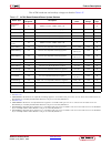
Ac701 evaluation board www.Xilinx.Com 69 ug952 (v1.3) april 7, 2015 feature descriptions table 1-32 shows the ac701 ti power system configuration for controller u9. Table 1-32: controller u9 power system configuration sequencer schematic regulator type voltage current page page contents net name #2 ...
Page 70
70 www.Xilinx.Com ac701 evaluation board ug952 (v1.3) april 7, 2015 chapter 1: ac701 evaluation board features figure 1-45 shows the power system for ucd90120a u9 controller #2 rails 1 through 5. X-ref target - figure 1-45 figure 1-45: u9 controller #2 ucd90120a power system ug952_c1_1 3 8_0 3 0615 ...
Page 71
Ac701 evaluation board www.Xilinx.Com 71 ug952 (v1.3) april 7, 2015 feature descriptions the lmz31503 and lmz31700 family adjustable voltage regulators have their output voltage set by an external resistor. The regulator topology on the ac701 board permits the ucd90120a to monitor rail voltage and c...
Page 72
72 www.Xilinx.Com ac701 evaluation board ug952 (v1.3) april 7, 2015 chapter 1: ac701 evaluation board features figure 1-46 shows the xadc external multiplexer block diagram. X-ref target - figure 1-46 figure 1-46: xadc external multiplexer block diagram ug952_c1_1 3 9_01181 3 1. ..._xadc_p/n =remote...
Page 73
Ac701 evaluation board www.Xilinx.Com 73 ug952 (v1.3) april 7, 2015 feature descriptions table 1-33 and table 1-34 list the ac701 board xadc power system voltage and current measurement details for the external muxes u14 and u13. Table 1-33: xadc measurements through mux u14 measurement type rail na...
Page 74
74 www.Xilinx.Com ac701 evaluation board ug952 (v1.3) april 7, 2015 chapter 1: ac701 evaluation board features i mgtavtt cs 0a-1.5a u23 100 0v-0.756v mgtavtt_xadc_cs_p 25 s7a 110 mgtavtt_xadc_cs_n 5 s7b not used, not connected not connected 26 s8a 111 not connected 4 s8b table 1-34: xadc measurement...
Page 75
Ac701 evaluation board www.Xilinx.Com 75 ug952 (v1.3) april 7, 2015 feature descriptions xadc header [ figure 1-2 , callout 31 ] 7 series fpgas provide an analog front end (xadc) block. The xadc block includes a dual 12-bit, 1 msps analog-to-digital convertor (adc) and on-chip sensors. See 7 series ...
Page 76
76 www.Xilinx.Com ac701 evaluation board ug952 (v1.3) april 7, 2015 chapter 1: ac701 evaluation board features for external measurements, an xadc header (j19) is provided. This header can be used to provide analog inputs to the fpga dedicated vp/vn channel, and to the vauxp[0]/ vauxn[0], vauxp[8]/va...
Page 77: Configuration Options
Ac701 evaluation board www.Xilinx.Com 77 ug952 (v1.3) april 7, 2015 configuration options configuration options the fpga on the ac701 board can be configured using these methods: • master spi flash memory (uses the quad spi flash memory u7). • jtag (uses the u26 digilent usb-to-jtag bridge or j4 dow...
Page 78
78 www.Xilinx.Com ac701 evaluation board ug952 (v1.3) april 7, 2015 chapter 1: ac701 evaluation board features figure 1-50 shows the quad spi flash memory u7 configuration circuit. X-ref target - figure 1-50 figure 1-50: ac701 board quad spi flash memory configuration circuit ug952_c1_42_07251 3 dq[...
Page 79: User Gpio Dip Switch Sw2
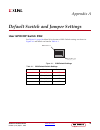
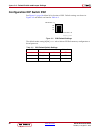
Ac701 evaluation board www.Xilinx.Com 79 ug952 (v1.3) april 7, 2015 appendix a default switch and jumper settings user gpio dip switch sw2 see figure 1-2, page 10 callout 23 for location of sw2. Default settings are shown in figure a-1 and details are listed in table a-1 . X-ref target - figure a-1 ...
Page 80
Appendix a: default switch and jumper settings 80 www.Xilinx.Com ac701 evaluation board ug952 (v1.3) april 7, 2015 configuration dip switch sw1 see figure 1-2, page 10 callout 28 for location of sw1. Default settings are shown in figure a-2 and details are listed in table a-2 . The default mode sett...
Page 81: Default Jumper Settings
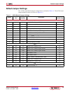
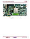
Default jumper settings ac701 evaluation board www.Xilinx.Com 81 ug952 (v1.3) april 7, 2015 default jumper settings the ac701 board default jumper configurations are listed in table a-3 . The ac701 board jumper header locations are shown in figure a-3 . Table a-3: ac701 default jumper settings callo...
Page 82
Appendix a: default switch and jumper settings 82 www.Xilinx.Com ac701 evaluation board ug952 (v1.3) april 7, 2015 x-ref target - figure a-3 figure a-3: ac701 board components (rev. 2.0) 8*bdb send feedback.
Page 83
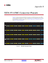
Ac701 evaluation board www.Xilinx.Com 83 ug952 (v1.3) april 7, 2015 appendix b vita 57.1 fmc connector pinouts figure b-1 shows the pinout of the fpga mezzanine card (fmc) high pin count (hpc) connector defined by the vita 57.1 fmc specification. For a description of how the ac701 board implements t...
Page 84
Appendix b: vita 57.1 fmc connector pinouts 84 www.Xilinx.Com ac701 evaluation board ug952 (v1.3) april 7, 2015 send feedback.
Page 85: Ac701 Board Xdc File Listing
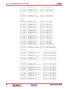
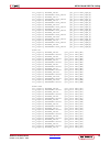
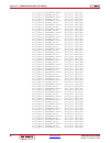
Ac701 evaluation board www.Xilinx.Com 85 ug952 (v1.3) april 7, 2015 appendix c master constraints file listing theac701 board master xilinx design constraints (xdc) file template provides for designs targeting the ac701 board. Net names in the constraints listed in the ac701 board xdc file listing c...
Page 86
Appendix c: master constraints file listing 86 www.Xilinx.Com ac701 evaluation board ug952 (v1.3) april 7, 2015 set_property package_pin d23 [get_ports rec_clock_c_p] set_property iostandard lvds_25 [get_ports rec_clock_c_p] set_property package_pin d24 [get_ports rec_clock_c_n] set_property iostand...
Page 87
Ac701 board xdc file listing ac701 evaluation board www.Xilinx.Com 87 ug952 (v1.3) april 7, 2015 set_property package_pin b1 [get_ports ddr3_dqs4_n] set_property iostandard diff_sstl15 [get_ports ddr3_dqs4_n] set_property package_pin v3 [get_ports ddr3_dqs3_p] set_property iostandard diff_sstl15 [ge...
Page 88
Appendix c: master constraints file listing 88 www.Xilinx.Com ac701 evaluation board ug952 (v1.3) april 7, 2015 set_property iostandard sstl15 [get_ports ddr3_d53] set_property package_pin k8 [get_ports ddr3_d52] set_property iostandard sstl15 [get_ports ddr3_d52] set_property package_pin k7 [get_po...
Page 89
Ac701 board xdc file listing ac701 evaluation board www.Xilinx.Com 89 ug952 (v1.3) april 7, 2015 set_property package_pin ab1 [get_ports ddr3_d23] set_property iostandard sstl15 [get_ports ddr3_d23] set_property package_pin ac1 [get_ports ddr3_d22] set_property iostandard sstl15 [get_ports ddr3_d22]...
Page 90
Appendix c: master constraints file listing 90 www.Xilinx.Com ac701 evaluation board ug952 (v1.3) april 7, 2015 set_property iostandard sstl15 [get_ports ddr3_a11] set_property package_pin n7 [get_ports ddr3_a10] set_property iostandard sstl15 [get_ports ddr3_a10] set_property package_pin k3 [get_po...
Page 91
Ac701 board xdc file listing ac701 evaluation board www.Xilinx.Com 91 ug952 (v1.3) april 7, 2015 #gpio lcd set_property package_pin l22 [get_ports lcd_db7_ls] set_property iostandard lvcmos33 [get_ports lcd_db7_ls] set_property package_pin m25 [get_ports lcd_db6_ls] set_property iostandard lvcmos33 ...
Page 92
Appendix c: master constraints file listing 92 www.Xilinx.Com ac701 evaluation board ug952 (v1.3) april 7, 2015 #gpio user sma set_property package_pin t8 [get_ports user_sma_gpio_p] set_property iostandard lvds_25 [get_ports user_sma_gpio_p] set_property package_pin t7 [get_ports user_sma_gpio_n] s...
Page 93
Ac701 board xdc file listing ac701 evaluation board www.Xilinx.Com 93 ug952 (v1.3) april 7, 2015 set_property package_pin e22 [get_ports xadc_gpio_1] set_property iostandard lvcmos25 [get_ports xadc_gpio_1] set_property package_pin h17 [get_ports xadc_gpio_0] set_property iostandard lvcmos25 [get_po...
Page 94
Appendix c: master constraints file listing 94 www.Xilinx.Com ac701 evaluation board ug952 (v1.3) april 7, 2015 set_property iostandard lvcmos25 [get_ports fmc1_hpc_la02_p] set_property package_pin h15 [get_ports fmc1_hpc_la02_n] set_property iostandard lvcmos25 [get_ports fmc1_hpc_la02_n] set_prope...
Page 95
Ac701 board xdc file listing ac701 evaluation board www.Xilinx.Com 95 ug952 (v1.3) april 7, 2015 set_property package_pin k21 [get_ports fmc1_hpc_la17_cc_p] set_property iostandard lvcmos25 [get_ports fmc1_hpc_la17_cc_p] set_property package_pin j21 [get_ports fmc1_hpc_la17_cc_n] set_property iostan...
Page 96
Appendix c: master constraints file listing 96 www.Xilinx.Com ac701 evaluation board ug952 (v1.3) april 7, 2015 set_property iostandard lvcmos25 [get_ports fmc1_hpc_la31_n] set_property package_pin h26 [get_ports fmc1_hpc_la32_p] set_property iostandard lvcmos25 [get_ports fmc1_hpc_la32_p] set_prope...
Page 97
Ac701 board xdc file listing ac701 evaluation board www.Xilinx.Com 97 ug952 (v1.3) april 7, 2015 set_property package_pin ac19 [get_ports fmc1_hpc_ha12_p] set_property iostandard lvcmos25 [get_ports fmc1_hpc_ha12_p] set_property package_pin ad19 [get_ports fmc1_hpc_ha12_n] set_property iostandard lv...
Page 98
Appendix c: master constraints file listing 98 www.Xilinx.Com ac701 evaluation board ug952 (v1.3) april 7, 2015 set_property iostandard lvcmos18 [get_ports hdmi_r_d31] set_property package_pin ab25 [get_ports hdmi_r_d30] set_property iostandard lvcmos18 [get_ports hdmi_r_d30] set_property package_pi...
Page 99
Ac701 board xdc file listing ac701 evaluation board www.Xilinx.Com 99 ug952 (v1.3) april 7, 2015 set_property package_pin v18 [get_ports phy_reset_b] set_property iostandard lvcmos18 [get_ports phy_reset_b] set_property package_pin w18 [get_ports phy_mdc] set_property iostandard lvcmos18 [get_ports ...
Page 100
Appendix c: master constraints file listing 100 www.Xilinx.Com ac701 evaluation board ug952 (v1.3) april 7, 2015 set_property iostandard lvds_25 [get_ports sfp_mgt_clk1_p] set_property package_pin ab11 [get_ports sfp_mgt_clk1_n] set_property iostandard lvds_25 [get_ports sfp_mgt_clk1_n] send feedbac...
Page 101: Board Setup
Ac701 evaluation board www.Xilinx.Com 101 ug952 (v1.3) april 7, 2015 appendix d board setup installing the ac701 board in a pc chassis installation of the ac701 board inside a computer chassis is required when developing or testing pci express® functionality. When the ac701 board is used inside a co...
Page 102
Appendix d: board setup 102 www.Xilinx.Com ac701 evaluation board ug952 (v1.3) april 7, 2015 8. Slide the ac701 board power switch sw15 to the on position. The pc can now be powered on. Send feedback.
Page 103: Board Specifications
Ac701 evaluation board www.Xilinx.Com 103 ug952 (v1.3) april 7, 2015 appendix e board specifications dimensions height 5.5 in. (14.0 cm) length 10.5 in. (26.7 cm) note: the ac701 board height exceeds the standard 4.376 in. (11.15 cm) height of a pci express card. Environmental temperature operating:...
Page 104
Appendix e: board specifications 104 www.Xilinx.Com ac701 evaluation board ug952 (v1.3) april 7, 2015 send feedback.
Page 105: Additional Resources
Ac701 evaluation board www.Xilinx.Com 105 ug952 (v1.3) april 7, 2015 appendix f additional resources xilinx resources for support resources such as answers, documentation, downloads, and forums, see the xilinx support website . To create a xilinx user account and sign up to receive automatic email n...
Page 106
106 www.Xilinx.Com ac701 evaluation board ug952 (v1.3) april 7, 2015 appendix f: additional resources 14. Ac701 si570 fixed frequencies ( xtp229 ) documents associated with other devices used by the ac701 board are available at these vendor websites: 15. Micron technology: www.Micron.Com (n25q256a13...
Page 107: Regulatory and Compliance
Ac701 evaluation board www.Xilinx.Com 107 ug952 (v1.3) april 7, 2015 appendix g regulatory and compliance information this product is designed and tested to conform to the european union directives and standards described in this section. Refer to the artix-7 fpga ac701 evaluation kit master answer ...
Page 108: Markings
108 www.Xilinx.Com ac701 evaluation board ug952 (v1.3) april 7, 2015 appendix g: regulatory and compliance information markings this product complies with directive 2002/96/ec on waste electrical and electronic equipment (weee). The affixed product label indicates that the user must not discard this...


