- DL manuals
- Xilinx
- Computer Hardware
- DS610
- Datasheet
Xilinx DS610 Datasheet
DS610 October 4, 2010
www.xilinx.com
Product Specification
1
© Copyright 2007–2010 Xilinx, Inc. XILINX, the Xilinx logo, Virtex, Spartan, ISE, and other designated brands included herein are trademarks of Xilinx in the United States and
other countries. PCI and PCI-X are trademarks of PCI-SIG and used under license. All other trademarks are the property of their respective owners.
Module 1:
Introduction and Ordering Information
DS610 (v3.0) October 4, 2010
•
Introduction
•
Features
•
Architectural Overview
•
Configuration Overview
•
General I/O Capabilities
•
Supported Packages and Package Marking
•
Ordering Information
Module 2:
Functional Description
DS610 (v3.0) October 4, 2010
The functionality of the Spartan®-3A DSP FPGA family is
described in the following documents.
•
UG331
:
Spartan-3 Generation FPGA User Guide
•
Clocking Resources
•
Digital Clock Managers (DCMs)
•
Block RAM
•
Configurable Logic Blocks (CLBs)
-
Distributed RAM
-
SRL16 Shift Registers
-
Carry and Arithmetic Logic
•
I/O Resources
•
Programmable Interconnect
•
ISE® Software Design Tools and IP Cores
•
Embedded Processing and Control Solutions
•
Pin Types and Package Overview
•
Package Drawings
•
Powering FPGAs
•
Power Management
•
UG332
:
Spartan-3 Generation Configuration User Guide
•
Configuration Overview
•
Configuration Pins and Behavior
•
Bitstream Sizes
•
Detailed Descriptions by Mode
-
Master Serial Mode using Platform Flash PROM
-
Master SPI Mode using Commodity Serial Flash
-
Master BPI Mode using Commodity Parallel Flash
-
Slave Parallel (SelectMAP) using a Processor
-
Slave Serial using a Processor
-
JTAG Mode
•
ISE iMPACT Programming Examples
•
MultiBoot Reconfiguration
•
Design Authentication using Device DNA
•
UG431
:
XtremeDSP™ DSP48A for Spartan-3A DSP
FPGAs User Guide
•
DSP48A Slice Design Considerations
•
DSP48A Architecture Highlights
-
18 x 18-Bit Multipliers
-
48-Bit Accumulator
-
18-bit Pre-Adder
•
DSP48A Application Examples
Module 3:
DC and Switching Characteristics
DS610 (v3.0) October 4, 2010
•
DC Electrical Characteristics
•
Absolute Maximum Ratings
•
Supply Voltage Specifications
•
Recommended Operating Conditions
•
Switching Characteristics
•
I/O Timing
•
Configurable Logic Block (CLB) Timing
•
Digital Clock Manager (DCM) Timing
•
Block RAM Timing
•
XtremeDSP Slice Timing
•
Configuration and JTAG Timing
Module 4:
Pinout Descriptions
DS610 (v3.0) October 4, 2010
•
Pin Descriptions
•
Package Overview
•
Pinout Tables
•
Footprint Diagrams
1
Spartan-3A DSP FPGA Family Data Sheet
DS610 October 4, 2010
Product Specification
Summary of DS610
Page 1
Ds610 october 4, 2010 www.Xilinx.Com product specification 1 © copyright 2007–2010 xilinx, inc. Xilinx, the xilinx logo, virtex, spartan, ise, and other designated brands included herein are trademarks of xilinx in the united states and other countries. Pci and pci-x are trademarks of pci-sig and us...
Page 2: Spartan-3A Dsp Fpga Family:
Ds610 (v3.0) october 4, 2010 www.Xilinx.Com product specification 2 © copyright 2007–2010 xilinx, inc. Xilinx, the xilinx logo, virtex, spartan, ise, and other designated brands included herein are trademarks of xilinx in the united states and other countries. Pci and pci-x are trademarks of pci-sig...
Page 3
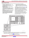
Spartan-3a dsp fpga family: introduction and ordering information ds610 (v3.0) october 4, 2010 www.Xilinx.Com product specification 3 architectural overview the spartan-3a dsp family architecture consists of five fundamental programmable functional elements: • xtremedsp™ dsp48a slice provides an 18-...
Page 4
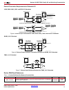
Spartan-3a dsp fpga family: introduction and ordering information ds610 (v3.0) october 4, 2010 www.Xilinx.Com product specification 4 configuration spartan-3a dsp fpgas are programmed by loading configuration data into robust, reprogrammable, static cmos configuration latches (ccls) that collectivel...
Page 5
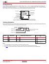
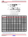
Spartan-3a dsp fpga family: introduction and ordering information ds610 (v3.0) october 4, 2010 www.Xilinx.Com product specification 5 package marking figure 2 shows the top marking for spartan-3a dsp fpgas. The “ 5c ” and “ 4i ” speed grade/temperature range part combinations may be dual marked as “...
Page 6
Spartan-3a dsp fpga family: introduction and ordering information ds610 (v3.0) october 4, 2010 www.Xilinx.Com product specification 6 revision history the following table shows the revision history for this document. Notice of disclaimer the xilinx hardware fpga and cpld devices referred to herein (...
Page 7: Spartan-3A Dsp Fpga Family:
Ds610 (v3.0) october 4, 2010 www.Xilinx.Com product specification 7 © copyright 2007–2010 xilinx, inc. Xilinx, the xilinx logo, virtex, spartan, ise, and other designated brands included herein are trademarks of xilinx in the united states and other countries. Pci and pci-x are trademarks of pci-sig...
Page 8
Spartan-3a dsp fpga family: functional description ds610 (v3.0) october 4, 2010 www.Xilinx.Com product specification 8 revision history the following table shows the revision history for this document. Notice of disclaimer the xilinx hardware fpga and cpld devices referred to herein (“products”) are...
Page 9: Spartan-3A Dsp Fpga Family:
Ds610 (v3.0) october 4, 2010 www.Xilinx.Com product specification 9 © copyright 2007–2010 xilinx, inc. Xilinx, the xilinx logo, virtex, spartan, ise, and other designated brands included herein are trademarks of xilinx in the united states and other countries. Pci and pci-x are trademarks of pci-sig...
Page 10
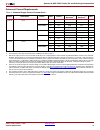
Spartan-3a dsp fpga family: dc and switching characteristics ds610 (v3.0) october 4, 2010 www.Xilinx.Com product specification 10 power supply specifications table 4: supply voltage thresholds for power-on reset symbol description min max units v ccintt threshold for the v ccint supply 0.4 1.0 v v c...
Page 11
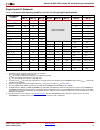
Spartan-3a dsp fpga family: dc and switching characteristics ds610 (v3.0) october 4, 2010 www.Xilinx.Com product specification 11 general recommended operating conditions table 7: general recommended operating conditions symbol description min nominal max units t j junction temperature commercial 0 ...
Page 12
Spartan-3a dsp fpga family: dc and switching characteristics ds610 (v3.0) october 4, 2010 www.Xilinx.Com product specification 12 general dc characteristics for i/o pins table 8: general dc characteristics of user i/o, dual-purpose, and dedicated pins (1) symbol description test conditions min typ m...
Page 13
Spartan-3a dsp fpga family: dc and switching characteristics ds610 (v3.0) october 4, 2010 www.Xilinx.Com product specification 13 quiescent current requirements table 9: quiescent supply current characteristics (1) symbol description device power typical (2) commercial maximum (2) industrial maximum...
Page 14
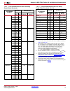
Spartan-3a dsp fpga family: dc and switching characteristics ds610 (v3.0) october 4, 2010 www.Xilinx.Com product specification 14 single-ended i/o standards table 10: recommended operating conditions for user i/os using single-ended standards iostandard attribute v cco for drivers (2) v ref v il v i...
Page 15
Spartan-3a dsp fpga family: dc and switching characteristics ds610 (v3.0) october 4, 2010 www.Xilinx.Com product specification 15 table 11: dc characteristics of user i/os using single-ended standards iostandard attribute test conditions logic level characteristics i ol (ma) i oh (ma) v ol max (v) v...
Page 16
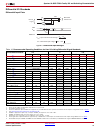
Spartan-3a dsp fpga family: dc and switching characteristics ds610 (v3.0) october 4, 2010 www.Xilinx.Com product specification 16 differential i/o standards differential input pairs x-ref target - figure 3 figure 3: differential input voltages table 12: recommended operating conditions for user i/os...
Page 17
Spartan-3a dsp fpga family: dc and switching characteristics ds610 (v3.0) october 4, 2010 www.Xilinx.Com product specification 17 differential output pairs x-ref target - figure 4 figure 4: differential output voltages table 13: dc characteristics of user i/os using differential signal standards ios...
Page 18
Spartan-3a dsp fpga family: dc and switching characteristics ds610 (v3.0) october 4, 2010 www.Xilinx.Com product specification 18 external termination requirements for differential i/o lvds, rsds, mini_lvds, and ppds i/o standards blvds_25 i/o standard tmds_33 i/o standard device dna read endurance ...
Page 19
Spartan-3a dsp fpga family: dc and switching characteristics ds610 (v3.0) october 4, 2010 www.Xilinx.Com product specification 19 switching characteristics all spartan-3a dsp fpgas ship in two speed grades: –4 and the higher performance –5. Switching characteristics in this document are designated a...
Page 20
Spartan-3a dsp fpga family: dc and switching characteristics ds610 (v3.0) october 4, 2010 www.Xilinx.Com product specification 20 i/o timing pin-to-pin clock-to-output times table 17: pin-to-pin clock-to-output times for the iob output path symbol description conditions device speed grade units -5 -...
Page 21
Spartan-3a dsp fpga family: dc and switching characteristics ds610 (v3.0) october 4, 2010 www.Xilinx.Com product specification 21 pin-to-pin setup and hold times table 18: pin-to-pin setup and hold times for the iob input path (system synchronous) symbol description conditions device speed grade uni...
Page 22
Spartan-3a dsp fpga family: dc and switching characteristics ds610 (v3.0) october 4, 2010 www.Xilinx.Com product specification 22 input setup and hold times table 19: setup and hold times for the iob input path symbol description conditions delay_ value device speed units -5 -4 min min setup times t...
Page 23
Spartan-3a dsp fpga family: dc and switching characteristics ds610 (v3.0) october 4, 2010 www.Xilinx.Com product specification 23 t ioickpd time from the active transition at the iclk input of the input flip-flop (iff) to the point where data must be held at the input pin. The input delay is program...
Page 24
Spartan-3a dsp fpga family: dc and switching characteristics ds610 (v3.0) october 4, 2010 www.Xilinx.Com product specification 24 input propagation times table 21: propagation times for the iob input path symbol description conditions delay_value device speed grade units -5 -4 max max propagation ti...
Page 25
Spartan-3a dsp fpga family: dc and switching characteristics ds610 (v3.0) october 4, 2010 www.Xilinx.Com product specification 25 t iopli the time it takes for data to travel from the input pin through the iff latch to the i output with no input delay programmed lvcmos25 (2) 0 xc3sd1800a 1.79 2.04 n...
Page 26
Spartan-3a dsp fpga family: dc and switching characteristics ds610 (v3.0) october 4, 2010 www.Xilinx.Com product specification 26 input timing adjustments table 22: input timing adjustments by iostandard convert input time from lvcmos25 to the following signal standard (iostandard) add the adjustmen...
Page 27
Spartan-3a dsp fpga family: dc and switching characteristics ds610 (v3.0) october 4, 2010 www.Xilinx.Com product specification 27 output propagation times table 23: timing for the iob output path symbol description conditions device speed grade units -5 -4 max max clock-to-output times t iockp when ...
Page 28
Spartan-3a dsp fpga family: dc and switching characteristics ds610 (v3.0) october 4, 2010 www.Xilinx.Com product specification 28 three-state output propagation times table 24: timing for the iob three-state path symbol description conditions device speed grade units -5 -4 max max synchronous output...
Page 29
Spartan-3a dsp fpga family: dc and switching characteristics ds610 (v3.0) october 4, 2010 www.Xilinx.Com product specification 29 output timing adjustments table 25: output timing adjustments for iob convert output time from lvcmos25 with 12ma drive and fast slew rate to the following signal standar...
Page 30
Spartan-3a dsp fpga family: dc and switching characteristics ds610 (v3.0) october 4, 2010 www.Xilinx.Com product specification 30 lvcmos25 slow 2 ma 5.33 5.33 ns 4 ma 2.81 2.81 ns 6 ma 2.82 2.82 ns 8 ma 1.14 1.14 ns 12 ma 1.10 1.10 ns 16 ma 0.83 0.83 ns 24 ma 2.26 (3) 2.26 (3) ns fast 2 ma 4.36 4.36...
Page 31
Spartan-3a dsp fpga family: dc and switching characteristics ds610 (v3.0) october 4, 2010 www.Xilinx.Com product specification 31 lvcmos12 slow 2 ma 7.14 7.14 ns 4 ma 4.87 4.87 ns 6 ma 5.67 5.67 ns fast 2 ma 6.77 6.77 ns 4 ma 5.02 5.02 ns 6 ma 4.09 4.09 ns quietio 2 ma 50.76 50.76 ns 4 ma 43.17 43.1...
Page 32
Spartan-3a dsp fpga family: dc and switching characteristics ds610 (v3.0) october 4, 2010 www.Xilinx.Com product specification 32 timing measurement methodology when measuring timing parameters at the programmable i/os, different signal standards call for different test conditions. Table 26 lists th...
Page 33
Spartan-3a dsp fpga family: dc and switching characteristics ds610 (v3.0) october 4, 2010 www.Xilinx.Com product specification 33 the capacitive load (c l ) is connected between the output and gnd. The output timing for all standards, as published in the speed files and the data sheet, is always bas...
Page 34
Spartan-3a dsp fpga family: dc and switching characteristics ds610 (v3.0) october 4, 2010 www.Xilinx.Com product specification 34 using ibis models to simulate load conditions in application ibis models permit the most accurate prediction of timing delays for a given application. The parameters foun...
Page 35
Spartan-3a dsp fpga family: dc and switching characteristics ds610 (v3.0) october 4, 2010 www.Xilinx.Com product specification 35 table 28: recommended simultaneously switching outputs per v cco /gnd pair (v ccaux = 3.3v) signal standard (iostandard) package type cs484, fg676 top, bottom (banks 0, 2...
Page 36
Spartan-3a dsp fpga family: dc and switching characteristics ds610 (v3.0) october 4, 2010 www.Xilinx.Com product specification 36 lvcmos25 slow 2 76 76 4 46 46 6 33 33 8 24 24 12 18 18 16 – 11 24 – 7 fast 2 18 18 4 14 14 6 6 6 8 6 6 12 3 3 16 – 3 24 – 2 quietio 2 76 76 4 60 60 6 48 48 8 36 36 12 36 ...
Page 37
Spartan-3a dsp fpga family: dc and switching characteristics ds610 (v3.0) october 4, 2010 www.Xilinx.Com product specification 37 lvcmos12 slow 2 40 40 4 – 25 6 – 18 fast 2 31 31 4 – 13 6 – 9 quietio 2 55 55 4 – 36 6 – 36 pci33_3 16 16 pci66_3 – 13 hstl_i – 20 hstl_iii – 8 hstl_i_18 17 17 hstl_ii_18...
Page 38
Spartan-3a dsp fpga family: dc and switching characteristics ds610 (v3.0) october 4, 2010 www.Xilinx.Com product specification 38 configurable logic block (clb) timing table 29: clb (slicem) timing symbol description speed grade units -5 -4 min max min max clock-to-output times t cko when reading fr...
Page 39
Spartan-3a dsp fpga family: dc and switching characteristics ds610 (v3.0) october 4, 2010 www.Xilinx.Com product specification 39 table 30: clb distributed ram switching characteristics symbol description speed grade units -5 -4 min max min max clock-to-output times t shcko time from the active edge...
Page 40
Spartan-3a dsp fpga family: dc and switching characteristics ds610 (v3.0) october 4, 2010 www.Xilinx.Com product specification 40 clock buffer/multiplexer switching characteristics table 32: clock distribution switching characteristics symbol description minimum maximum units speed grade -5 -4 t gio...
Page 41
Spartan-3a dsp fpga family: dc and switching characteristics ds610 (v3.0) october 4, 2010 www.Xilinx.Com product specification 41 block ram timing table 33: block ram timing symbol description speed grade units -5 -4 min max min max clock-to-output times t rcko_doa_nc when reading from block ram, th...
Page 42
Spartan-3a dsp fpga family: dc and switching characteristics ds610 (v3.0) october 4, 2010 www.Xilinx.Com product specification 42 dsp48a timing to reference the dsp48a block diagram, see ug431 : xtremedsp dsp48a for spartan-3a dsp fpga user guide . Table 34: setup times for the dsp48a symbol descrip...
Page 43
Spartan-3a dsp fpga family: dc and switching characteristics ds610 (v3.0) october 4, 2010 www.Xilinx.Com product specification 43 table 35: clock to out, propagation delays, and maximum frequency for the dsp48a symbol description pre-adder multiplier post-adder speed grade units -5 -4 max max clock ...
Page 44
Spartan-3a dsp fpga family: dc and switching characteristics ds610 (v3.0) october 4, 2010 www.Xilinx.Com product specification 44 digital clock manager (dcm) timing for specification purposes, the dcm consists of three key components: the delay-locked loop (dll), the digital frequency synthesizer (d...
Page 45
Spartan-3a dsp fpga family: dc and switching characteristics ds610 (v3.0) october 4, 2010 www.Xilinx.Com product specification 45 table 37: switching characteristics for the dll symbol description device speed grade units -5 -4 min max min max output frequency ranges clkout_freq_clk0 frequency for t...
Page 46
Spartan-3a dsp fpga family: dc and switching characteristics ds610 (v3.0) october 4, 2010 www.Xilinx.Com product specification 46 digital frequency synthesizer (dfs) delay lines dcm_delay_step (5) finest delay resolution, averaged over all steps all 15 35 15 35 ps notes: 1. The numbers in this table...
Page 47
Spartan-3a dsp fpga family: dc and switching characteristics ds610 (v3.0) october 4, 2010 www.Xilinx.Com product specification 47 table 39: switching characteristics for the dfs symbol description device speed grade units -5 -4 min max min max output frequency ranges clkout_freq_fx (2) frequency for...
Page 48
Spartan-3a dsp fpga family: dc and switching characteristics ds610 (v3.0) october 4, 2010 www.Xilinx.Com product specification 48 phase shifter (ps) miscellaneous dcm timing table 40: recommended operating conditions for the ps in variable phase mode symbol description speed grade units -5 -4 min ma...
Page 49
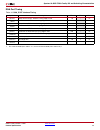
Spartan-3a dsp fpga family: dc and switching characteristics ds610 (v3.0) october 4, 2010 www.Xilinx.Com product specification 49 dna port timing table 43: dna_port interface timing symbol description min max units t dnassu setup time on shift before the rising edge of clk 1.0 – ns t dnash hold time...
Page 50
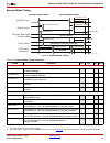
Spartan-3a dsp fpga family: dc and switching characteristics ds610 (v3.0) october 4, 2010 www.Xilinx.Com product specification 50 suspend mode timing x-ref target - figure 9 figure 9: suspend mode timing table 44: suspend mode timing parameters symbol description min typ max units entering suspend m...
Page 51
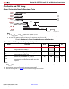
Spartan-3a dsp fpga family: dc and switching characteristics ds610 (v3.0) october 4, 2010 www.Xilinx.Com product specification 51 configuration and jtag timing general configuration power-on/reconfigure timing x-ref target - figure 10 figure 10: waveforms for power-on and the beginning of configurat...
Page 52
Spartan-3a dsp fpga family: dc and switching characteristics ds610 (v3.0) october 4, 2010 www.Xilinx.Com product specification 52 configuration clock (cclk) characteristics table 46: master mode cclk output period by configrate option setting symbol description configrate setting (1) temperature ran...
Page 53
Spartan-3a dsp fpga family: dc and switching characteristics ds610 (v3.0) october 4, 2010 www.Xilinx.Com product specification 53 table 47: master mode cclk output frequency by configrate option setting symbol description configrate setting temperature range minimum maximum units f cclk1 equivalent ...
Page 54
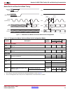
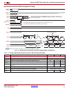
Spartan-3a dsp fpga family: dc and switching characteristics ds610 (v3.0) october 4, 2010 www.Xilinx.Com product specification 54 master serial and slave serial mode timing x-ref target - figure 11 figure 11: waveforms for master serial and slave serial configuration table 50: timing for the master ...
Page 55
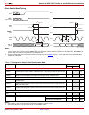
Spartan-3a dsp fpga family: dc and switching characteristics ds610 (v3.0) october 4, 2010 www.Xilinx.Com product specification 55 slave parallel mode timing x-ref target - figure 12 figure 12: waveforms for slave parallel configuration table 51: timing for the slave parallel configuration mode symbo...
Page 56
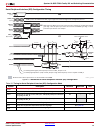
Spartan-3a dsp fpga family: dc and switching characteristics ds610 (v3.0) october 4, 2010 www.Xilinx.Com product specification 56 serial peripheral interface (spi) configuration timing x-ref target - figure 13 figure 13: waveforms for serial peripheral interface (spi) configuration table 52: timing ...
Page 57
Spartan-3a dsp fpga family: dc and switching characteristics ds610 (v3.0) october 4, 2010 www.Xilinx.Com product specification 57 table 53: configuration timing requirements for attached spi serial flash symbol description requirement units t ccs spi serial flash prom chip-select time ns t dsu spi s...
Page 58
Spartan-3a dsp fpga family: dc and switching characteristics ds610 (v3.0) october 4, 2010 www.Xilinx.Com product specification 58 byte peripheral interface (bpi) configuration timing x-ref target - figure 14 figure 14: waveforms for byte-wide peripheral interface (bpi) configuration table 54: timing...
Page 59
Spartan-3a dsp fpga family: dc and switching characteristics ds610 (v3.0) october 4, 2010 www.Xilinx.Com product specification 59 table 55: configuration timing requirements for attached parallel nor bpi flash symbol description requirement units t ce (t elqv ) parallel nor flash prom chip-select ti...
Page 60
Spartan-3a dsp fpga family: dc and switching characteristics ds610 (v3.0) october 4, 2010 www.Xilinx.Com product specification 60 ieee 1149.1/1532 jtag test access port timing x-ref target - figure 15 figure 15: jtag waveforms table 56: timing for the jtag (2) test access port symbol description all...
Page 61
Spartan-3a dsp fpga family: dc and switching characteristics ds610 (v3.0) october 4, 2010 www.Xilinx.Com product specification 61 revision history the following table shows the revision history for this document. Date version revision 04/02/07 1.0 initial xilinx release. 05/25/07 1.0.1 minor edits. ...
Page 62: Spartan-3A Dsp Fpga Family:
Ds610 (v3.0) october 4, 2010 www.Xilinx.Com product specification 62 © copyright 2007–2010 xilinx, inc. Xilinx, the xilinx logo, virtex, spartan, ise, and other designated brands included herein are trademarks of xilinx in the united states and other countries. Pci and pci-x are trademarks of pci-si...
Page 63
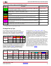
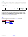
Spartan-3a dsp fpga family: pinout descriptions ds610 (v3.0) october 4, 2010 www.Xilinx.Com product specification 63 package pins by type each package has three separate voltage supply inputs—vccint, vccaux, and vcco—and a common ground return, gnd. The numbers of pins dedicated to these functions v...
Page 64
Spartan-3a dsp fpga family: pinout descriptions ds610 (v3.0) october 4, 2010 www.Xilinx.Com product specification 64 electronic versions of the package pinout tables and foot- prints are available for download from the xilinx® website. Using a spreadsheet program, the data can be sorted and reformat...
Page 65
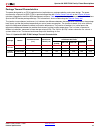
Spartan-3a dsp fpga family: pinout descriptions ds610 (v3.0) october 4, 2010 www.Xilinx.Com product specification 65 package thermal characteristics the power dissipated by an fpga application has implications on package selection and system design. The power consumed by a spartan-3a dsp fpga is rep...
Page 66
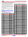
Spartan-3a dsp fpga family: pinout descriptions ds610 (v3.0) october 4, 2010 www.Xilinx.Com product specification 66 cs484: 484-ball chip-scale ball grid array the 484-ball chip-scale ball grid array, cs484, supports both the xc3sd1800a and xc3sd3400a fpgas. There are no pinout differences between t...
Page 67
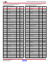
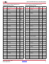
Spartan-3a dsp fpga family: pinout descriptions ds610 (v3.0) october 4, 2010 www.Xilinx.Com product specification 67 0 io_l19p_0/gclk8 f10 gclk 0 io_l17n_0/gclk5 f11 gclk 0 ip_0 f12 input 0 io_l13n_0 f13 i/o 0 io_l13p_0 f14 i/o 0 io_l05n_0 f15 i/o 0 io_l04n_0 f16 i/o 0 io_l23p_0 g8 i/o 0 vcco_0 b5 v...
Page 68
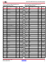
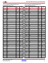
Spartan-3a dsp fpga family: pinout descriptions ds610 (v3.0) october 4, 2010 www.Xilinx.Com product specification 68 1 io_l03n_1/a1 v20 dual 1 ip_l08p_1 v22 input 1 io_l03p_1/a0 w19 dual 1 ip_l04n_1/vref_1 w20 vref 1 ip_l04p_1 w21 input 1 io_l06p_1 w22 i/o 1 io_l02p_1/ldc1 y21 dual 1 io_l06n_1 y22 i...
Page 69
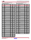
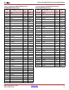
Spartan-3a dsp fpga family: pinout descriptions ds610 (v3.0) october 4, 2010 www.Xilinx.Com product specification 69 2 ip_2/vref_2 y14 vref 2 io_l24n_2/d3 y15 dual 2 io_l29n_2 y16 i/o 2 io_l29p_2 y17 i/o 2 io_l26p_2/d2 y18 dual 2 io_l26n_2/d1 y19 dual 2 vcco_2 aa5 vcco 2 vcco_2 aa9 vcco 2 vcco_2 aa1...
Page 70
Spartan-3a dsp fpga family: pinout descriptions ds610 (v3.0) october 4, 2010 www.Xilinx.Com product specification 70 3 io_l36p_3 v4 i/o 3 io_l35n_3 w1 i/o 3 io_l37n_3 w2 i/o 3 io_l37p_3 w3 i/o 3 io_l35p_3 y1 i/o 3 ip_l39p_3 y2 input 3 vcco_3 e2 vcco 3 vcco_3 j2 vcco 3 vcco_3 j5 vcco 3 vcco_3 n2 vcco...
Page 71
Spartan-3a dsp fpga family: pinout descriptions ds610 (v3.0) october 4, 2010 www.Xilinx.Com product specification 71 gnd gnd t14 gnd gnd gnd t15 gnd gnd gnd t19 gnd gnd gnd t21 gnd gnd gnd u6 gnd gnd gnd u11 gnd gnd gnd u17 gnd gnd gnd w7 gnd gnd gnd w12 gnd gnd gnd w16 gnd gnd gnd y3 gnd gnd gnd y2...
Page 72
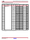
Spartan-3a dsp fpga family: pinout descriptions ds610 (v3.0) october 4, 2010 www.Xilinx.Com product specification 72 user i/os by bank table 64 and table 65 indicates how the user-i/o pins are distributed between the four i/o banks on the cs484 package. The awake pin is counted as a dual-purpose i/o...
Page 73
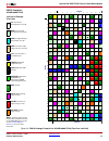
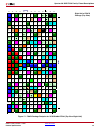
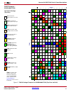
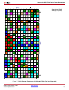
Spartan-3a dsp fpga family: pinout descriptions ds610 (v3.0) october 4, 2010 www.Xilinx.Com product specification 73 cs484 footprint left half of package (top view) 156 i/o: unrestricted, general-purpose user i/o. 41 input: unrestricted, general-purpose input pin. 51 dual: configuration pins, then p...
Page 74
Spartan-3a dsp fpga family: pinout descriptions ds610 (v3.0) october 4, 2010 www.Xilinx.Com product specification 74 right half of cs484 package (top view) figure 16: cs484 package footprint (top view–right half) 12 13 14 15 16 17 18 19 20 21 22 input i/o l11p_0 i/o l10p_0 input i/o l06p_0 vref_0 i/...
Page 75
Spartan-3a dsp fpga family: pinout descriptions ds610 (v3.0) october 4, 2010 www.Xilinx.Com product specification 75 fg676: 676-ball fine-pitch ball grid array the 676-ball fine-pitch ball grid array, fg676, supports both the xc3sd1800a and the xc3sd3400a fpgas. There are multiple pinout differences...
Page 76
Spartan-3a dsp fpga family: pinout descriptions ds610 (v3.0) october 4, 2010 www.Xilinx.Com product specification 76 0 ip_0/vref_0 d14 vref 0 io_l22p_0 d16 i/o 0 io_l21p_0 d17 i/o 0 io_l17p_0 d18 i/o 0 io_l11p_0 d20 i/o 0 io_l10n_0 d21 i/o 0 io_l05p_0 d22 i/o 0 io_l06p_0 d23 i/o 0 io_l44p_0 c5 i/o 0...
Page 77
Spartan-3a dsp fpga family: pinout descriptions ds610 (v3.0) october 4, 2010 www.Xilinx.Com product specification 77 0 vcco_0 b11 vcco 0 vcco_0 b16 vcco 0 vcco_0 b22 vcco 1 io_l01p_1/hdc y20 dual 1 io_l01n_1/ldc2 y21 dual 1 io_l13p_1 y22 i/o 1 io_l13n_1 y23 i/o 1 io_l15p_1 y24 i/o 1 io_l15n_1 y25 i/...
Page 78
Spartan-3a dsp fpga family: pinout descriptions ds610 (v3.0) october 4, 2010 www.Xilinx.Com product specification 78 1 io_l50n_1 k21 i/o 1 io_l46n_1 k22 i/o 1 io_l46p_1 k23 i/o 1 ip_l40p_1 k24 input 1 io_l41p_1 k25 i/o 1 io_l41n_1 k26 i/o 1 io_l59p_1 j19 i/o 1 io_l59n_1 j20 i/o 1 io_l62p_1/a20 j21 d...
Page 79
Spartan-3a dsp fpga family: pinout descriptions ds610 (v3.0) october 4, 2010 www.Xilinx.Com product specification 79 2 io_l46p_2 w17 i/o 2 io_l09p_2 v10 i/o 2 io_l13p_2 v11 i/o 2 io_l16p_2 v12 i/o 2 io_l20p_2 v13 i/o 2 io_l31p_2 v14 i/o 2 io_l35p_2 v15 i/o 2 io_l42p_2 v16 i/o 2 io_l46n_2 v17 i/o 2 i...
Page 80
Spartan-3a dsp fpga family: pinout descriptions ds610 (v3.0) october 4, 2010 www.Xilinx.Com product specification 80 2 io_l41n_2 ac20 i/o 2 io_l45n_2 ac21 i/o 2 io_2 ac22 i/o 2 ip_2/vref_2 ab6 vref 2 io_l14n_2 ab7 i/o 2 io_l15p_2 ab9 i/o 2 io_l21p_2 ab12 i/o 2 ip_2 ab13 input 2 io_l30n_2/mosi/csi_b ...
Page 81
Spartan-3a dsp fpga family: pinout descriptions ds610 (v3.0) october 4, 2010 www.Xilinx.Com product specification 81 3 io_l48p_3 t10 i/o 3 io_l36p_3/vref_3 r1 vref 3 io_l36n_3 r2 i/o 3 io_l37p_3 r3 i/o 3 io_l37n_3 r4 i/o 3 io_l40p_3 r5 i/o 3 io_l40n_3 r6 i/o 3 io_l45n_3 r7 i/o 3 io_l45p_3 r8 i/o 3 i...
Page 82
Spartan-3a dsp fpga family: pinout descriptions ds610 (v3.0) october 4, 2010 www.Xilinx.Com product specification 82 3 ip_l04p_3 c2 input 3 io_l02n_3 b1 i/o 3 io_l02p_3 b2 i/o 3 ip_l66p_3 ae1 input 3 ip_l66n_3/vref_3 ae2 vref 3 io_l65p_3 ad1 i/o 3 io_l65n_3 ad2 i/o 3 io_l60n_3 ac1 i/o 3 io_l64p_3 ac...
Page 83
Spartan-3a dsp fpga family: pinout descriptions ds610 (v3.0) october 4, 2010 www.Xilinx.Com product specification 83 gnd gnd f21 gnd gnd gnd f26 gnd gnd gnd c3 gnd gnd gnd c9 gnd gnd gnd c14 gnd gnd gnd c19 gnd gnd gnd c24 gnd gnd gnd af1 gnd gnd gnd af6 gnd gnd gnd af11 gnd gnd gnd af16 gnd gnd gnd...
Page 84
Spartan-3a dsp fpga family: pinout descriptions ds610 (v3.0) october 4, 2010 www.Xilinx.Com product specification 84 user i/os by bank table 67 indicates how the available user-i/o pins are distributed between the four i/o banks on the fg676 package. The awake pin is counted as a dual-purpose i/o. T...
Page 85
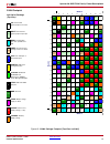
Spartan-3a dsp fpga family: pinout descriptions ds610 (v3.0) october 4, 2010 www.Xilinx.Com product specification 85 fg676 footprint – xc3sd1800a fpga left half of package (top view) 314 i/o: unrestricted, general-purpose user i/o. 82 input: unrestricted, general-purpose input pin. 51 dual: configur...
Page 86
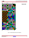
Spartan-3a dsp fpga family: pinout descriptions ds610 (v3.0) october 4, 2010 www.Xilinx.Com product specification 86 right half of fg676 package (top view) figure 17: fg676 package footprint for xc3sd1800a fpga (top view–right half) 14 15 16 17 18 19 20 21 22 23 24 25 26 i/o l26n_0 gclk7 i/o l23n_0 ...
Page 87
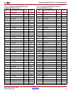
Spartan-3a dsp fpga family: pinout descriptions ds610 (v3.0) october 4, 2010 www.Xilinx.Com product specification 87 xc3sd3400a fpga table 68 lists all the fg676 package pins for the xc3sd3400a fpga. They are sorted by bank number and then by pin name. Pairs of pins that form a differential i/o pair...
Page 88
Spartan-3a dsp fpga family: pinout descriptions ds610 (v3.0) october 4, 2010 www.Xilinx.Com product specification 88 0 io_l10n_0 d21 i/o 0 io_l05p_0 d22 i/o 0 io_l06p_0 d23 i/o 0 io_l44p_0 c5 i/o 0 io_l41n_0 c6 i/o 0 io_l42n_0 c7 i/o 0 io_l40p_0 c8 i/o 0 io_l34p_0 c10 i/o 0 io_l32p_0 c11 i/o 0 io_l3...
Page 89
Spartan-3a dsp fpga family: pinout descriptions ds610 (v3.0) october 4, 2010 www.Xilinx.Com product specification 89 1 io_l12n_1 u18 i/o 1 io_l12p_1 u19 i/o 1 io_l10n_1 u20 i/o 1 io_l14p_1 u21 i/o 1 io_l21n_1 u22 i/o 1 io_l23p_1 u23 i/o 1 io_l23n_1/vref_1 u24 vref 1 ip_1/vref_1 u26 vref 1 io_l17n_1 ...
Page 90
Spartan-3a dsp fpga family: pinout descriptions ds610 (v3.0) october 4, 2010 www.Xilinx.Com product specification 90 1 ip_1/vref_1 g25 vref 1 io_l58p_1/vref_1 f22 vref 1 io_l56n_1 f23 i/o 1 io_l54n_1 f24 i/o 1 io_l54p_1 f25 i/o 1 io_l56p_1 e24 i/o 1 io_l60p_1 e26 i/o 1 io_l61n_1 d24 i/o 1 io_l61p_1 ...
Page 91
Spartan-3a dsp fpga family: pinout descriptions ds610 (v3.0) october 4, 2010 www.Xilinx.Com product specification 91 2 io_l48p_2 af23 i/o 2 io_l52p_2/d0/din/miso af24 dual 2 io_l51p_2 af25 i/o 2 io_l06p_2 ae3 i/o 2 io_l07p_2 ae4 i/o 2 io_l10n_2 ae6 i/o 2 io_l11n_2 ae7 i/o 2 io_l18p_2 ae8 i/o 2 io_l1...
Page 92
Spartan-3a dsp fpga family: pinout descriptions ds610 (v3.0) october 4, 2010 www.Xilinx.Com product specification 92 2 vcco_2 ab8 vcco 2 vcco_2 ab14 vcco 2 vcco_2 ab19 vcco 3 io_l53p_3 y1 i/o 3 io_l53n_3 y2 i/o 3 ip_3 y3 input 3 io_l57p_3 y5 i/o 3 io_l57n_3 y6 i/o 3 ip_l50p_3 w1 input 3 ip_l50n_3/vr...
Page 93
Spartan-3a dsp fpga family: pinout descriptions ds610 (v3.0) october 4, 2010 www.Xilinx.Com product specification 93 3 io_l23n_3 k2 i/o 3 io_l23p_3 k3 i/o 3 io_l22n_3 k4 i/o 3 io_l22p_3 k5 i/o 3 io_l18p_3 k6 i/o 3 io_l13p_3 k7 i/o 3 io_l05n_3 k8 i/o 3 io_l05p_3 k9 i/o 3 ip_l24p_3 j1 input 3 ip_l20n_...
Page 94
Spartan-3a dsp fpga family: pinout descriptions ds610 (v3.0) october 4, 2010 www.Xilinx.Com product specification 94 gnd gnd p12 gnd gnd gnd p16 gnd gnd gnd p19 gnd gnd gnd p24 gnd gnd gnd n3 gnd gnd gnd n8 gnd gnd gnd n11 gnd gnd gnd n15 gnd gnd gnd m12 gnd gnd gnd m14 gnd gnd gnd m16 gnd gnd gnd l...
Page 95
Spartan-3a dsp fpga family: pinout descriptions ds610 (v3.0) october 4, 2010 www.Xilinx.Com product specification 95 gnd gnd a23 gnd gnd gnd a26 gnd vccaux suspend v20 pwrmgmt vccaux done ab21 config vccaux prog_b a2 config vccaux tdi g7 jtag vccaux tdo e23 jtag vccaux tms d4 jtag vccaux tck a25 jta...
Page 96
Spartan-3a dsp fpga family: pinout descriptions ds610 (v3.0) october 4, 2010 www.Xilinx.Com product specification 96 user i/os by bank table 69 indicates how the available user-i/o pins are distributed between the four i/o banks on the fg676 package. The awake pin is counted as a dual-purpose i/o. T...
Page 97
Spartan-3a dsp fpga family: pinout descriptions ds610 (v3.0) october 4, 2010 www.Xilinx.Com product specification 97 fg676 footprint – xc3sd3400a fpga left half of package (top view) 314 i/o: unrestricted, general-purpose user i/o. 34 input: unrestricted, general-purpose input pin. 51 dual: configur...
Page 98
Spartan-3a dsp fpga family: pinout descriptions ds610 (v3.0) october 4, 2010 www.Xilinx.Com product specification 98 right half of fg676 package (top view) figure 17: fg676 package footprint for xc3sd3400a fpga (top view–right half) 14 15 16 17 18 19 20 21 22 23 24 25 26 i/o l26n_0 gclk7 i/o l23n_0 ...
Page 99
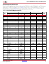
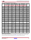
Spartan-3a dsp fpga family: pinout descriptions ds610 (v3.0) october 4, 2010 www.Xilinx.Com product specification 99 footprint migration differences there are multiple migration footprint differences between the xc3sd1800a and the xc3sd3400a in the fg676 package. These migration footprint difference...
Page 100
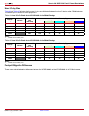
Spartan-3a dsp fpga family: pinout descriptions ds610 (v3.0) october 4, 2010 www.Xilinx.Com product specification 100 migration recommendations there are multiple pinout differences between the xc3sd1800a and the xc3sd3400a fpgas in the fg676 package. Please note the differences between the two devi...
Page 101
Spartan-3a dsp fpga family: pinout descriptions ds610 (v3.0) october 4, 2010 www.Xilinx.Com product specification 101 revision history the following table shows the revision history for this document. Date version revision 04/02/07 1.0 initial xilinx release. 05/25/07 1.1 updates to table 59 , table...

