- DL manuals
- Xilinx
- Computer Hardware
- LogiCORE IP AXI
- Product Manual
Xilinx LogiCORE IP AXI Product Manual
Summary of LogiCORE IP AXI
Page 1
Logicore ip axi bridge for pci express v2.4 product guide vivado design suite pg055 june 4, 2014.
Page 2
Axi bridge for pci express v2.4 www.Xilinx.Com 2 pg055 june 4, 2014 table of contents ip facts chapter 1: overview feature summary. . . . . . . . . . . . . . . . . . . . . . . . . . . . . . . . . . . . . . . . . . . . . . . . . . . . . . . . . . . . . . . . . . 6 unsupported features. . . . . . . . ...
Page 3
Axi bridge for pci express v2.4 www.Xilinx.Com 3 pg055 june 4, 2014 simulation . . . . . . . . . . . . . . . . . . . . . . . . . . . . . . . . . . . . . . . . . . . . . . . . . . . . . . . . . . . . . . . . . . . . . . 79 synthesis and implementation . . . . . . . . . . . . . . . . . . . . . . . . ....
Page 4: Introduction
Axi bridge for pci express v2.4 www.Xilinx.Com 4 pg055 june 4, 2014 product specification introduction the xilinx ® logicore™ ip axi root port/ endpoint (rp/ep) bridge for pci express® core is an interface between the axi4 and pci express. Definitions and references are provided in this document for...
Page 5
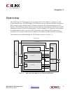
Axi bridge for pci express v2.4 www.Xilinx.Com 5 pg055 june 4, 2014 chapter 1 overview the axi bridge for pci express® core is designed for the vivado® ip integrator in the vivado design suite. The axi bridge for pci express core provides an interface between an axi4 customer user interface and pci ...
Page 6: Feature Summary
Axi bridge for pci express v2.4 www.Xilinx.Com 6 pg055 june 4, 2014 chapter 1: overview feature summary the axi bridge for pci express core is an interface between the axi4 and pci express. It contains the memory mapped axi4 to axi4-stream bridge and the axi4-stream enhanced interface block for pcie...
Page 7
Axi bridge for pci express v2.4 www.Xilinx.Com 7 pg055 june 4, 2014 chapter 1: overview licensing and ordering information this xilinx® logicore™ ip module is provided at no additional cost with the xilinx vivado design suite under the terms of the xilinx end user license. Information about this and...
Page 8
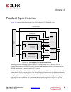
Axi bridge for pci express v2.4 www.Xilinx.Com 8 pg055 june 4, 2014 chapter 2 product specification figure 2-1 shows the architecture of the axi bridge for pci express® core. The register block contains registers used in the axi bridge for pci express core for dynamically mapping the axi4 memory map...
Page 9: Standards
Axi bridge for pci express v2.4 www.Xilinx.Com 9 pg055 june 4, 2014 chapter 2: product specification configured max payload size setting, which are passed to the integrated block for pci express. A second remote axi master initiated write request write address and qualifiers can then be captured and...
Page 10: Performance
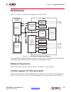
Axi bridge for pci express v2.4 www.Xilinx.Com 10 pg055 june 4, 2014 chapter 2: product specification performance figure 2-2 shows a configuration diagram for a target fpga. The target fpga is filled with logic to drive the lookup table (lut) and block ram utilization to approximately 70% and the i/...
Page 11: Resource Utilization
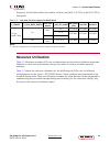
Axi bridge for pci express v2.4 www.Xilinx.Com 11 pg055 june 4, 2014 chapter 2: product specification frequency, the axi data width, the number of lanes, and gen1 (2.5 gt/s) or gen2 (5.0 gt/s) link speed. Resource utilization table 2-2 illustrates a subset of ip core configurations and the device ut...
Page 12: Port Descriptions
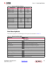
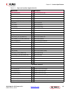
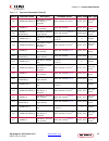
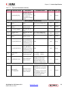
Axi bridge for pci express v2.4 www.Xilinx.Com 12 pg055 june 4, 2014 chapter 2: product specification port descriptions the interface signals for the axi bridge for pci express are described in table 2-3 . Table 2-2: resource utilization summary configuration slice registers slice luts endpoint x1 g...
Page 13
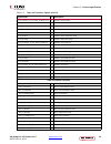
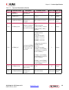
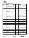
Axi bridge for pci express v2.4 www.Xilinx.Com 13 pg055 june 4, 2014 chapter 2: product specification s_axi_awburst[1:0] i slave write burst type s_axi_awvalid i slave address write valid s_axi_awready o slave address write ready s_axi_wdata[c_s_axi_data_width-1:0] i slave write data s_axi_wstrb[c_s...
Page 14
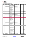
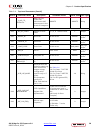
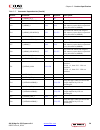
Axi bridge for pci express v2.4 www.Xilinx.Com 14 pg055 june 4, 2014 chapter 2: product specification m_axi_wstrb[c_m_axi_data_width/8-1:0] o master write strobe m_axi_wlast o master write last m_axi_wvalid o master write valid m_axi_wready i master write ready m_axi_bresp[1:0] i master write respon...
Page 15: Bridge Parameters
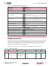
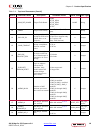
Axi bridge for pci express v2.4 www.Xilinx.Com 15 pg055 june 4, 2014 chapter 2: product specification bridge parameters because many features in the axi bridge for pci express core design can be parameterized, you are able to uniquely tailor the implementation of the core using only the resources re...
Page 16
Axi bridge for pci express v2.4 www.Xilinx.Com 16 pg055 june 4, 2014 chapter 2: product specification c_xlnx_ref_board target fpga board none kc705_reva kc705_revb kc705_revc vc707 none string g1 c_family target fpga family kintex7, virtex7, artix7, zynq string g2 c_include_rc configures the axi bri...
Page 17
Axi bridge for pci express v2.4 www.Xilinx.Com 17 pg055 june 4, 2014 chapter 2: product specification g10 c_axibar2pciebar_0 pcie bar to which axi bar_0 is mapped valid address for pcie (2) 0xffff_ffff std_logic_ vector g11 c_axibar_1 axi bar_1 aperture low address valid axi address (1)(3)(4) 0xffff...
Page 18
Axi bridge for pci express v2.4 www.Xilinx.Com 18 pg055 june 4, 2014 chapter 2: product specification g28 c_axibar_ highaddr_5 axi bar_5 aperture high address valid axi address (1)(3)(4) 0x0000_0000 std_logic_ vector g29 c_axibar_as_5 axi bar_5 address size 0: 32 bit 1: 64 bit 0 integer g30 c_axibar...
Page 19
Axi bridge for pci express v2.4 www.Xilinx.Com 19 pg055 june 4, 2014 chapter 2: product specification c_pciebar2axibar_0 _sec defines the axibar memory space (pcie bar_0) (accessible from pcie) to be either secure or non-secure memory mapped. 0: denotes a non-secure memory space 1: marks the axi mem...
Page 20
Axi bridge for pci express v2.4 www.Xilinx.Com 20 pg055 june 4, 2014 chapter 2: product specification c_s_axi_ctl_ protocol axi4-lite port connection definition to axi interconnect in the vivado ip integrator. Axi4lite axi4lite string core for pcie configuration parameters g41 c_no_of_lanes number o...
Page 21
Axi bridge for pci express v2.4 www.Xilinx.Com 21 pg055 june 4, 2014 chapter 2: product specification c_num_msi_req specifies the size of the msi request vector for selecting the number of requested message values. 0-5 0 integer memory mapped axi4 parameters g50 c_m_axi_data_ width axi master bus da...
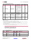
Page 22: Parameter Dependencies
Axi bridge for pci express v2.4 www.Xilinx.Com 22 pg055 june 4, 2014 chapter 2: product specification parameter dependencies table 2-5 lists the parameter dependencies. G58 num_read_ outstanding axi interconnect slave port read pipeline depth 1: only one active axi araddr can be accepted in axi slav...
Page 23
Axi bridge for pci express v2.4 www.Xilinx.Com 23 pg055 june 4, 2014 chapter 2: product specification g4 c_include_baroffset_reg g10 , g14 , g18 , g22 , g26 , g30 g6 if g4 = 0, then g10, g14, g18, g22, g26 and g30 have no meaning. The number of registers included is set by g6. G5 c_supports_narrow_ ...
Page 24
Axi bridge for pci express v2.4 www.Xilinx.Com 24 pg055 june 4, 2014 chapter 2: product specification g21 c_axibar_as_3 g6 g22 c_axibar2pciebar_3 g4 , g6 meaningful when g4 = 1. G23 c_axibar_4 g24 g24 g23 and g24 define the range in axi-memory space that is responded to by this device (axibar) g24 c...
Page 25
Axi bridge for pci express v2.4 www.Xilinx.Com 25 pg055 june 4, 2014 chapter 2: product specification table 2-6 summarizes the relationship between the ip design parameters, c_family and c_pcie_use_mode. The c_pcie_use_mode is used to specify the 7 series (and derivative fpga technology) serial tran...
Page 26: Memory Map
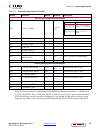
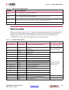
Axi bridge for pci express v2.4 www.Xilinx.Com 26 pg055 june 4, 2014 chapter 2: product specification memory map the memory map shown in table 2-7 shows the address mapping for the axi bridge for pci express core. These registers are described in more detail in the following section. All registers a...
Page 27
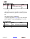
Axi bridge for pci express v2.4 www.Xilinx.Com 27 pg055 june 4, 2014 chapter 2: product specification pcie configuration space header the pcie configuration space header is a memory aperture for accessing the core for pcie configuration space. For 7 series devices, this area is read-only when config...
Page 28
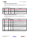
Axi bridge for pci express v2.4 www.Xilinx.Com 28 pg055 june 4, 2014 chapter 2: product specification vsec header register (offset 0x12c) the vsec header register (described in table 2-9 ) provides a unique (within a given vendor) identifier for the layout and contents of the vsec structure, as well...
Page 29
Axi bridge for pci express v2.4 www.Xilinx.Com 29 pg055 june 4, 2014 chapter 2: product specification bridge status and control register (offset 0x134) the bridge status and control register (described in table 2-11 ) provides information about the current state of the axi4-stream bridge. It also pr...
Page 30
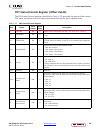
Axi bridge for pci express v2.4 www.Xilinx.Com 30 pg055 june 4, 2014 chapter 2: product specification table 2-12: interrupt decode register bits name core access reset value description 0 link down rw1c 0 indicates that link-up on the pci express link was lost. Not asserted unless link-up had previo...
Page 31
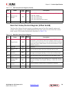
Axi bridge for pci express v2.4 www.Xilinx.Com 31 pg055 june 4, 2014 chapter 2: product specification interrupt mask register (offset 0x13c) the interrupt mask register controls whether each individual interrupt source can cause the interrupt line to be asserted. A one in any location allows the int...
Page 32
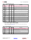
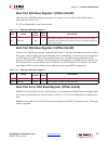
Axi bridge for pci express v2.4 www.Xilinx.Com 32 pg055 june 4, 2014 chapter 2: product specification bus location register (offset 0x140) the bus location register reports the bus, device, and function number, and the port number for the pcie port ( table 2-14 ). 16 intx interrupt received ro 0 ena...
Page 33
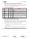
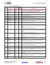
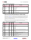
Axi bridge for pci express v2.4 www.Xilinx.Com 33 pg055 june 4, 2014 chapter 2: product specification phy status/control register (offset 0x144) the phy status/control register (described in table 2-15 ) provides the status of the current phy state, as well as control of speed and rate switching for...
Page 34
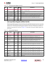
Axi bridge for pci express v2.4 www.Xilinx.Com 34 pg055 june 4, 2014 chapter 2: product specification root port status/control register (offset 0x148) the root port status/control register provides access to root port specific status and control. This register is only implemented for root port cores...
Page 35
Axi bridge for pci express v2.4 www.Xilinx.Com 35 pg055 june 4, 2014 chapter 2: product specification root port msi base register 1 (offset 0x14c) the root port msi base register contains the upper 32-bits of the 64-bit msi address (described in table 2-17 ). For ep configurations, read returns zero...
Page 36
Axi bridge for pci express v2.4 www.Xilinx.Com 36 pg055 june 4, 2014 chapter 2: product specification root port interrupt fifo read register 1 (offset 0x158) reads from this location return queued interrupt messages. Data from each read follows the format shown in table 2-20 . For msi interrupts, th...
Page 37
Axi bridge for pci express v2.4 www.Xilinx.Com 37 pg055 june 4, 2014 chapter 2: product specification root port interrupt fifo read register 2 (offset 0x15c) reads from this location return queued interrupt messages. Data from each read follows the format shown in table 2-21 . For msi interrupts, th...
Page 38: 0X208 - 0X234)
Axi bridge for pci express v2.4 www.Xilinx.Com 38 pg055 june 4, 2014 chapter 2: product specification axi base address translation configuration registers (offset 0x208 - 0x234) the axi base address translation configuration registers and their offsets are shown in table 2-24 and the register bits a...
Page 39
Axi bridge for pci express v2.4 www.Xilinx.Com 39 pg055 june 4, 2014 chapter 2: product specification table 2-25: axi base address translation configuration register bit definitions bits name core access reset value description 31-0 lower address r/w c_axibar2pciebar_0(31 to 0) to create the address...
Page 40
Axi bridge for pci express v2.4 www.Xilinx.Com 40 pg055 june 4, 2014 chapter 2: product specification enhanced configuration access when the axi bridge for pci express core is configured as a root port, configuration traffic is generated by using the pci express enhanced configuration access mechani...
Page 41: Unsupported Memory Space
Axi bridge for pci express v2.4 www.Xilinx.Com 41 pg055 june 4, 2014 chapter 2: product specification (c_include_rc = 0), the underlying integrated block configuration space and the core memory map are available at the beginning of the memory space. The memory space looks like a simple pci express c...
Page 42: General Design Guidelines
Axi bridge for pci express v2.4 www.Xilinx.Com 42 pg055 june 4, 2014 chapter 3 designing with the core this chapter includes guidelines and additional information to make designing with the core easier. General design guidelines the xilinx® vivado® design suite has been optimized to provide a starti...
Page 43: Resets
Axi bridge for pci express v2.4 www.Xilinx.Com 43 pg055 june 4, 2014 chapter 3: designing with the core the refclk input must be provided at the frequency selected by the value of c_ref_clk_freq . This clock is used to generate the two output clocks and is also the clock used to drive the axi4 bus. ...
Page 44: Shared Logic
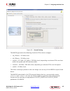
Axi bridge for pci express v2.4 www.Xilinx.Com 44 pg055 june 4, 2014 chapter 3: designing with the core shared logic this new feature allows you to share common blocks across multiple instantiations. It minimizes the amount of required hdl modifications. You can use your own system-level clocking or...
Page 45
Axi bridge for pci express v2.4 www.Xilinx.Com 45 pg055 june 4, 2014 chapter 3: designing with the core the mmcm generates the following clocks for pcie solution wrapper: • clk_125mhz - 125 mhz clock. • clk_250mhz - 250 mhz clock. • userclk - 62.5 mhz / 125 mhz / 250 mhz clock, depending on selected...
Page 46: Shared Gt_Common
Axi bridge for pci express v2.4 www.Xilinx.Com 46 pg055 june 4, 2014 chapter 3: designing with the core tip: sharing the mmcm between pcie and other cores in your design saves fpga resources and eases output clock path routing. Limitations • reference clock input to mmcm is restricted to 100 mhz in ...
Page 47
Axi bridge for pci express v2.4 www.Xilinx.Com 47 pg055 june 4, 2014 chapter 3: designing with the core limitations • the reset logic in the pipe wrapper resets the qpll when the pcie block performs a rate change. When sharing is enabled, the core/logic which is sharing the qpll must be able to hand...
Page 48
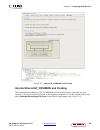
Axi bridge for pci express v2.4 www.Xilinx.Com 48 pg055 june 4, 2014 chapter 3: designing with the core internal shared gt_common and clocking this feature allows sharing of gt_common and clocks while these modules are still internal to the core (not brought up to the support wrapper). It can be ena...
Page 49
Axi bridge for pci express v2.4 www.Xilinx.Com 49 pg055 june 4, 2014 chapter 3: designing with the core x-ref target - figure 3-6 figure 3-6: internal shared logic send feedback.
Page 50: Clocking Interface
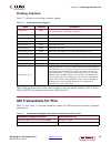
Axi bridge for pci express v2.4 www.Xilinx.Com 50 pg055 june 4, 2014 chapter 3: designing with the core clocking interface table 3-2 defines the clocking interface signals. The clocking architecture is described in detail in the use model chapter of the 7 series fpgas gtx/gth transceivers user guide...
Page 51
Axi bridge for pci express v2.4 www.Xilinx.Com 51 pg055 june 4, 2014 chapter 3: designing with the core transaction ordering for pcie the axi bridge for pci express core conforms to strict pcie transaction ordering rules. See the pcie v2.1 specification [ref 5] for the complete rule set. The followi...
Page 52: Address Translation
Axi bridge for pci express v2.4 www.Xilinx.Com 52 pg055 june 4, 2014 chapter 3: designing with the core the read data being returned on the axi bus. Timing is based off the axi awvalid signal timing relative to the axi rvalid assertion. Any axi write transaction in which awvalid was asserted before ...
Page 53
Axi bridge for pci express v2.4 www.Xilinx.Com 53 pg055 june 4, 2014 chapter 3: designing with the core example 1 (32-bit pcie address mapping) this example shows the generic settings to set up four independent 32-bit axi bars and address translation of axi addresses to a remote address space for pc...
Page 54
Axi bridge for pci express v2.4 www.Xilinx.Com 54 pg055 june 4, 2014 chapter 3: designing with the core example 2 (64-bit pcie address mapping) this example shows the generic settings to set up to three independent 64-bit axi bars and address translation of axi addresses to a remote address space fo...
Page 55
Axi bridge for pci express v2.4 www.Xilinx.Com 55 pg055 june 4, 2014 chapter 3: designing with the core • accessing bridge pciebar_1 with address 0xa00000001235fedc on the bus for pcie yields 0xfe35fedc on the axi bus. Example 4 this example shows the generic settings to set up a combination of two ...
Page 56: Interrupts
Axi bridge for pci express v2.4 www.Xilinx.Com 56 pg055 june 4, 2014 chapter 3: designing with the core • accessing the bridge axibar_0 with address 0x12340abc on the axi bus yields 0x56710abc on the bus for pcie. • accessing the bridge axibar_1 with address 0xabcdf123 on the axi bus yields 0x500000...
Page 57: Msi Interrupt
Axi bridge for pci express v2.4 www.Xilinx.Com 57 pg055 june 4, 2014 chapter 3: designing with the core msi interrupt when the msi_enable output pin indicates that the bridge has endpoint msi functionality enabled ( msi_enable = ‘1’), the intx_msi_request input pin is defined as msi_request and can ...
Page 58: Legacy Interrupts
Axi bridge for pci express v2.4 www.Xilinx.Com 58 pg055 june 4, 2014 chapter 3: designing with the core additional ip is required in the endpoint pcie system to create the prioritization scheme for the msi vectors on the pcie interface. Legacy interrupts the bridge supports legacy interrupts for pci...
Page 59
Axi bridge for pci express v2.4 www.Xilinx.Com 59 pg055 june 4, 2014 chapter 3: designing with the core illegal burst type the slave bridge monitors axi read and write burst type inputs to ensure that only the incr (incrementing burst) type is requested. Any other value on these inputs is treated as...
Page 60
Axi bridge for pci express v2.4 www.Xilinx.Com 60 pg055 june 4, 2014 chapter 3: designing with the core poison bit received on completion packet an error poison occurs when the completion tlp ep bit is set, indicating that there is poisoned data in the payload. When the slave bridge detects the pois...
Page 61
Axi bridge for pci express v2.4 www.Xilinx.Com 61 pg055 june 4, 2014 chapter 3: designing with the core axi decerr response when the master bridge receives a decerr response from the axi bus, the request is discarded and the master decerr (mde) interrupt is asserted. If the request was non-posted, a...
Page 62: Link Down Behavior
Axi bridge for pci express v2.4 www.Xilinx.Com 62 pg055 june 4, 2014 chapter 3: designing with the core link down behavior the normal operation of the axi bridge for pci express core is dependent on the integrated block for pcie establishing and maintaining the point-to-point link with an external d...
Page 63: Power Limit Message Tlp
Axi bridge for pci express v2.4 www.Xilinx.Com 63 pg055 june 4, 2014 chapter 3: designing with the core power limit message tlp the axi bridge for pci express core automatically sends a power limit message tlp when the master enable bit of the command register is set. The software must set the reque...
Page 64
Axi bridge for pci express v2.4 www.Xilinx.Com 64 pg055 june 4, 2014 chapter 3: designing with the core configuration transaction timeout configuration transactions are non-posted transactions. The axi bridge for pci express core has a timer for timeout termination of configuration transactions that...
Page 65
Axi bridge for pci express v2.4 www.Xilinx.Com 65 pg055 june 4, 2014 chapter 4 design flow steps this chapter describes customizing and generating the core, constraining the core, and the simulation, synthesis and implementation steps that are specific to this ip core. More detailed information abou...
Page 66: Customizing The Core
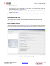
Axi bridge for pci express v2.4 www.Xilinx.Com 66 pg055 june 4, 2014 chapter 4: design flow steps for further details, see: • “working with ip” and “customizing ip for the design” in the vivado design suite user guide: designing with ip (ug896) [ref 9] . • “working with the vivado ide” section in th...
Page 67
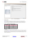
Axi bridge for pci express v2.4 www.Xilinx.Com 67 pg055 june 4, 2014 chapter 4: design flow steps component name base name of the output f iles generated for the core. The name must begin with a letter and can be composed of these characters: a to z, 0 to 9, and “_.” pcie device / port type indicate...
Page 68
Axi bridge for pci express v2.4 www.Xilinx.Com 68 pg055 june 4, 2014 chapter 4: design flow steps number of lanes the axi bridge for pci express® core requires the selection of the initial lane width. Table 4-1 defines the available widths and associated generated core. Wider lane width cores can tr...
Page 69
Axi bridge for pci express v2.4 www.Xilinx.Com 69 pg055 june 4, 2014 chapter 4: design flow steps pcie block location the axi bridge for pci express core allows the selection of the pci express hard block within xilinx fpgas. Pcie id settings the identity settings pages are shown in figure 4-3 . The...
Page 70
Axi bridge for pci express v2.4 www.Xilinx.Com 70 pg055 june 4, 2014 chapter 4: design flow steps unique. The default value, 10eeh , is the vendor id for xilinx. Enter your vendor identification number here. Ffffh is reserved. • device id : a unique identifier for the application; the default value,...
Page 71
Axi bridge for pci express v2.4 www.Xilinx.Com 71 pg055 june 4, 2014 chapter 4: design flow steps base address register overview the axi bridge for pci express core in endpoint configuration supports up to three 32-bit bars or three 64-bit bars. The axi memory mapped to pci express® in root port con...
Page 72
Axi bridge for pci express v2.4 www.Xilinx.Com 72 pg055 june 4, 2014 chapter 4: design flow steps all bar registers share these options: • checkbox : click the checkbox to enable the bar; deselect the checkbox to disable the bar. • type : bars can be memory apertures only. ° memory : memory bars can...
Page 73
Axi bridge for pci express v2.4 www.Xilinx.Com 73 pg055 june 4, 2014 chapter 4: design flow steps interrupt pin indicates the usage of legacy interrupts.The axi bridge for pci express core implements inta only. Msi vectors requested indicates the number of msi vectors requested by the core. Completi...
Page 74
Axi bridge for pci express v2.4 www.Xilinx.Com 74 pg055 june 4, 2014 chapter 4: design flow steps axi base address registers the axi base address registers (bars) screen shown in figure 4-6 sets the axi base address registers and the translation between axi memory space and pci express memory space....
Page 75
Axi bridge for pci express v2.4 www.Xilinx.Com 75 pg055 june 4, 2014 chapter 4: design flow steps aperture high address sets the upper address threshold for the address range associated to the bar. You should edit this parameter to fit design requirements. Axi to pcie translation configures the tran...
Page 76
Axi bridge for pci express v2.4 www.Xilinx.Com 76 pg055 june 4, 2014 chapter 4: design flow steps baseaddr sets the axi base address for the device. You should edit this parameter to fit design requirements. Highaddr sets the axi high address threshold for the device. You should edit this parameter ...
Page 77: Output Generation
Axi bridge for pci express v2.4 www.Xilinx.Com 77 pg055 june 4, 2014 chapter 4: design flow steps output generation for details, see “generating ip output products” in the vivado design suite user guide: designing with ip (ug896) [ref 9] . For information regarding the example design, see example de...
Page 78: Placement Constraints
Axi bridge for pci express v2.4 www.Xilinx.Com 78 pg055 june 4, 2014 chapter 4: design flow steps placement constraints the axi bridge for pci express core provides a xilinx design constraint (xdc) file for all supported pcie, part, and package permutations. You can find the generated xdc file in th...
Page 79: Clock Frequencies
Axi bridge for pci express v2.4 www.Xilinx.Com 79 pg055 june 4, 2014 chapter 4: design flow steps set_property loc gtpe2_channel_x*y* [get_cells {u0/comp_axi_enhanced_pcie/ comp_enhanced_core_top_wrap/axi_pcie_enhanced_core_top_i/pcie_7x_v2_0_inst/ gt_ges.Gt_top_i/pipe_wrapper_i/pipe_lane[0].Gt_wrap...
Page 80: Overview
Axi bridge for pci express v2.4 www.Xilinx.Com 80 pg055 june 4, 2014 chapter 5 example design this chapter contains information about the example design provided in the vivado® design suite. Overview the example simulation design for the endpoint configuration of the axi-pcie block consists of two d...
Page 81
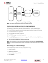
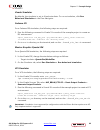
Axi bridge for pci express v2.4 www.Xilinx.Com 81 pg055 june 4, 2014 chapter 5: example design note: the example design supports verilog as the target language. Customizing and generating the example design in customize ip dialog box, make the following selections for the example design. 1. In the p...
Page 82
Axi bridge for pci express v2.4 www.Xilinx.Com 82 pg055 june 4, 2014 chapter 5: example design vivado simulator by defaults, the simulator is set to vivado simulator. To run a simulation, click run behavioral simulation in the flow navigator. Cadence ies for a cadence ies simulation, the following s...
Page 83: Example Design Elements
Axi bridge for pci express v2.4 www.Xilinx.Com 83 pg055 june 4, 2014 chapter 5: example design implementation design overview for implementation design, the axi-bram controller can be used as a scratch pad memory to write and read to block ram locations. Example design elements the core wrapper incl...
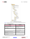
Page 84
Axi bridge for pci express v2.4 www.Xilinx.Com 84 pg055 june 4, 2014 chapter 5: example design table 5-1 provides a descriptions of the contents of the example design directories. Table 5-1: example design structure x-ref target - figure 5-2 figure 5-2: example design output structure directory desc...
Page 85
Axi bridge for pci express v2.4 www.Xilinx.Com 85 pg055 june 4, 2014 chapter 5: example design project_1/axi_pcie_0_example/ axi_pcie_0_example.Srcs/sim_1/imports/ simulation/functional contains the test bench file. Project_1/axi_pcie_0_example/ axi_pcie_0_example.Srcs/constrs_1/imports/ example_des...
Page 86
Axi bridge for pci express v2.4 www.Xilinx.Com 86 pg055 june 4, 2014 chapter 6 test bench for information about the test bench for the example design, see chapter 5, example design . Send feedback.
Page 87: Parameter Changes
Axi bridge for pci express v2.4 www.Xilinx.Com 87 pg055 june 4, 2014 appendix a migrating and upgrading this appendix contains information about migrating a design from ise ® design suite to the vivado ® design suite, and for upgrading to a more recent version of the ip core. For customers upgrading...
Page 88: Finding Help On Xilinx.Com
Axi bridge for pci express v2.4 www.Xilinx.Com 88 pg055 june 4, 2014 appendix b debugging this appendix provides information for using the resources available on the xilinx® support website, debug tools, and other step-by-step processes for debugging designs that use the axi bridge for pci express c...
Page 89: Contacting Technical Support
Axi bridge for pci express v2.4 www.Xilinx.Com 89 pg055 june 4, 2014 appendix b: debugging answer records are created and maintained daily ensuring that users have access to the most accurate information available. Answer records for this core are listed below, and can be located by using the search...
Page 90: Debug Tools
Axi bridge for pci express v2.4 www.Xilinx.Com 90 pg055 june 4, 2014 appendix b: debugging debug tools there are many tools available to address axi bridge for pci express design issues. It is important to know which tools are useful for debugging various situations. Vivado lab tool vivado® lab tool...
Page 91: Third-Party Tools
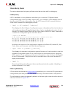
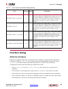
Axi bridge for pci express v2.4 www.Xilinx.Com 91 pg055 june 4, 2014 appendix b: debugging third-party tools this section describes third-party software tools that can be useful in debugging. Lspci (linux) lspci is available on linux platforms and allows you to view the pci express device configurat...
Page 92
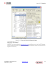
Axi bridge for pci express v2.4 www.Xilinx.Com 92 pg055 june 4, 2014 appendix b: debugging hwdirect (windows) hwdirect can be purchased at www.Eprotek.Com and allows you to view the pci express device configuration space as well as the extended configuration space (including the aer registers on the...
Page 93
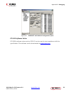
Axi bridge for pci express v2.4 www.Xilinx.Com 93 pg055 june 4, 2014 appendix b: debugging pci-sig software suites pci-sig® software suites such as pcie-cv can be used to test compliance with the specification. This software can be downloaded at www.Pcisig.Com . X-ref target - figure b-2 figure b-2:...
Page 94: Simulation Debug
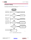
Axi bridge for pci express v2.4 www.Xilinx.Com 94 pg055 june 4, 2014 appendix b: debugging simulation debug the simulation debug flow for mentor graphics questa® sim is illustrated in figure b-3 . A similar approach can be used with other simulators. X-ref target - figure b-3 figure b-3: questa sim ...
Page 95: Hardware Debug
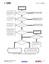
Axi bridge for pci express v2.4 www.Xilinx.Com 95 pg055 june 4, 2014 appendix b: debugging hardware debug hardware issues can range from device recognition issues to problems seen after hours of testing. This section provides debug flow diagrams for some of the most common issues. Endpoints that are...
Page 96
Axi bridge for pci express v2.4 www.Xilinx.Com 96 pg055 june 4, 2014 appendix b: debugging x-ref target - figure b-4 figure b-4: design fails in hardware debug flow diagram design fails in hardware does a soft reset fix the problem? (user_lnk_up = 1) no is user_reset deasserted? (user_reset = 0) no ...
Page 97: Link Is Training Debug
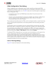
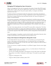
Axi bridge for pci express v2.4 www.Xilinx.Com 97 pg055 june 4, 2014 appendix b: debugging fpga configuration time debug device initialization and configuration issues can be caused by not having the fpga configured fast enough to enter link training and be recognized by the system. Section 6.6 of p...
Page 98
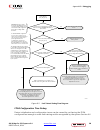
Axi bridge for pci express v2.4 www.Xilinx.Com 98 pg055 june 4, 2014 appendix b: debugging fpga configuration time debug device initialization and configuration issues can be caused by not having the fpga configured fast enough to enter link training and be recognized by the system. Section 6.6 x-re...
Page 99
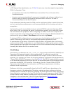
Axi bridge for pci express v2.4 www.Xilinx.Com 99 pg055 june 4, 2014 appendix b: debugging of pci express base specification, rev. 2.1 [ref 5] states two rules that might be impacted by fpga configuration time: • a component must enter the ltssm detect state within 20 ms of the end of the fundamenta...
Page 100
Axi bridge for pci express v2.4 www.Xilinx.Com 100 pg055 june 4, 2014 appendix b: debugging debugging pci configuration space parameters often, a user application fails to be recognized by the system, but the xilinx pio example design works. In these cases, the user application is often using a pci ...
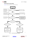
Page 101: Data Transfer Failing Debug
Axi bridge for pci express v2.4 www.Xilinx.Com 101 pg055 june 4, 2014 appendix b: debugging data transfer failing debug figure b-6 shows the flowchart for data transfer debug. X-ref target - figure b-6 figure b-6: data transfer debug flow diagram )sthesystemfreezingorhanging )suse?Lnk?Uptoggling .O ...
Page 102: Identifying Errors
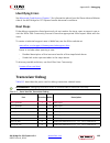
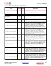
Axi bridge for pci express v2.4 www.Xilinx.Com 102 pg055 june 4, 2014 appendix b: debugging identifying errors see abnormal conditions in chapter 3 for information about how the slave side and master side of the axi bridge for pci express handle abnormal conditions. Next steps if the debug suggestio...
Page 103
Axi bridge for pci express v2.4 www.Xilinx.Com 103 pg055 june 4, 2014 appendix b: debugging pipe_sync_fsm_tx o should be examined if pipe_rst_fsm stuck at 11'b10000000000, or pipe_rate_fsm stuck at 24'b000100000000000000000000. Pipe_sync_fsm_rx o deprecated. Pipe_drp_fsm o should be examined if pipe...
Page 104: Interface Debug
Axi bridge for pci express v2.4 www.Xilinx.Com 104 pg055 june 4, 2014 appendix b: debugging interface debug axi4-lite interfaces read from a register that does not have all 0s as a default to verify that the interface is functional. Output s_axi_arready asserts when the read address is valid and out...
Page 105: Xilinx Resources
Axi bridge for pci express v2.4 www.Xilinx.Com 105 pg055 june 4, 2014 appendix c additional resources and legal notices xilinx resources for support resources such as answers, documentation, downloads, and forums, see xilinx support . For a glossary of technical terms used in xilinx documentation, s...
Page 106: Revision History
Axi bridge for pci express v2.4 www.Xilinx.Com 106 pg055 june 4, 2014 appendix c: additional resources and legal notices revision history the following table shows the revision history for this document. Please read: important legal notices the information disclosed to you hereunder (the "materials"...
Page 107
Axi bridge for pci express v2.4 www.Xilinx.Com 107 pg055 june 4, 2014 appendix c: additional resources and legal notices updates to the materials or to product specifications. You may not reproduce, modify, distribute, or publicly display the materials without prior written consent. Certain products...

