- DL manuals
- Xilinx
- Processor
- Zynq-7000
- User Manual
Xilinx Zynq-7000 User Manual - Core Architecture
Zynq-7000 AP SoC and 7 Series FPGAs MIS v4.1
90
UG586 November 30, 2016
Chapter 1: DDR3 and DDR2 SDRAM Memory Interface Solution
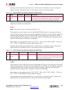
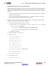
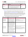
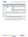
10. Run implementation flow with the Vivado tool. For details about implementation, see
the Vivado Design Suite User Guide: Designing with IP (UG896)
.
Note:
Similar steps can be followed for the user design using appropriate .dcp and .xdc files.
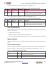
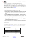
Core Architecture
This section describes the architecture of the 7 series FPGAs memory interface solutions
core, providing an overview of the core modules and interfaces.
Overview
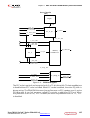
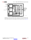
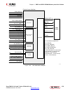
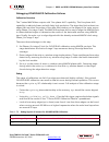
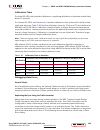
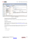
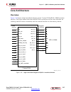
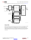
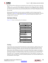
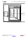
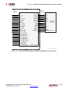
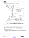
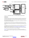
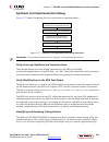
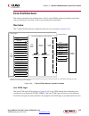
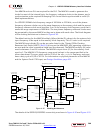
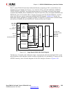
The 7 series FPGAs memory interface solutions core is shown in
.
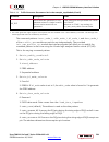
X-Ref Target - Figure 1-51
Figure 1-51:
7 Series FPGAs Memory Interface Solution
rst
clk
app_addr
app_cmd
app_en
app_hi_pri
app_wdf_data
app_wdf_end
app_wdf_mask
app_wdf_wren
app_rdy
app_rd_data
app_rd_data_end
app_rd_data_valid
app_wdf_rdy
app_sr_req
app_sr_active
app_ref_req
app_ref_ack
app_zq_req
app_zq_ack
ddr_ad dr
ddr_ba
ddr_cas_n
ddr_ck
ddr_cke
ddr_cs_n
ddr_dm
ddr_o dt
ddr_ra s_n
ddr_reset_n
ddr we n
ddr_dq
ddr_dqs_n
ddr_dqs
User
FPGA
Logic
DDR2/DDR3
SDRAM
User
Interface
Block
Memory
Controller
Physical
Layer
7 Series FPGAs Memory Interface Solution
User Interface
(1)
Physical Interface
7 Series FPGAs
Native Interface
MC/PHY Interface
ddr_ck_n
ddr_parity
IOB
1. System clock (sys_clk_p and sys_clk_n/sys_clk_i), Reference clock (clk_ref_p and clk_ref_n/clk_ref_i), and system reset (sys_rst_n) port
connections are not shown in block diagram.
Summary of Zynq-7000
Page 1
Zynq-7000 ap soc and 7 series devices memory interface solutions v4.1 user guide ug586 november 30, 2016.
Page 2
Zynq-7000 ap soc and 7 series fpgas mis v4.1 2 ug586 november 30, 2016 www.Xilinx.Com date version revision 11/30/2016 4.1 • renamed questasim to questa advanced simulator. Qdr ii+ • updated qdr_k_n/p directions in physical interface signals table. • updated in qdr_k_n/p directions i/o standards tab...
Page 3
Zynq-7000 ap soc and 7 series fpgas mis v4.1 3 ug586 november 30, 2016 www.Xilinx.Com 11/18/2015 2.4 • added asynchronous to sys_rst in all sections. • added note to relaxed mode in ddr3/ddr2 and lddr2 sections. • updated code in all configuration sections • added important jitter note in pinout req...
Page 4
Zynq-7000 ap soc and 7 series fpgas mis v4.1 4 ug586 november 30, 2016 www.Xilinx.Com 04/01/2015 2.3 • updated description in all configuration sections. • updated sim_bypass_init_cal. Chapter 1 • added description in setting ddr3 memory parameter option section. • added note to answer record: 54025...
Page 5
Zynq-7000 ap soc and 7 series fpgas mis v4.1 5 ug586 november 30, 2016 www.Xilinx.Com 11/19/2014 2.3 chapter 1 • updated description in round-robin section. • updated rtt_wr in table 1-92: 7 series fpga memory solution configuration parameters. • updated description in debugging oclkdelayed calibrat...
Page 6
Zynq-7000 ap soc and 7 series fpgas mis v4.1 6 ug586 november 30, 2016 www.Xilinx.Com 06/04/2014 2.1 chapter 1 • added reference to data sheet in features section. • added important note about data mask in controller options section. • added note in precharge policy section. • added prbs_saddr_ mask...
Page 7
Zynq-7000 ap soc and 7 series fpgas mis v4.1 7 ug586 november 30, 2016 www.Xilinx.Com 04/02/2014 2.0 chapter 1 • updated book to dqs. • updated table 1-4: files in example_design/sim directory. • updated file description in simulation flow using ies and vcs script files section. • added no buffer de...
Page 8
Zynq-7000 ap soc and 7 series fpgas mis v4.1 8 ug586 november 30, 2016 www.Xilinx.Com 12/18/2013 2.0 • vivado design suite release only for mig v2.0. Chapter 1 • added out of context content. • updated table 1-4: modules in example_design/sim directory. • updated /user_design section. • updated fig....
Page 9
Zynq-7000 ap soc and 7 series fpgas mis v4.1 9 ug586 november 30, 2016 www.Xilinx.Com 10/02/2013 2.0 • vivado design suite release only for mig v2.0. • removed ise content throughout book and updated screenshots to v2.0. Chapter 1 • updated memory part bullet description. • updated table 1-4 sim.Do ...
Page 10
Zynq-7000 ap soc and 7 series fpgas mis v4.1 10 ug586 november 30, 2016 www.Xilinx.Com 06/19/2013 2.0 • vivado design suite release only for mig v2.0. Revision number advanced to 2.0 to align with core version number. Chapter 1 • updated chipscope to vivado logic analyzer, vio, and ila. • updated ui...
Page 11
Zynq-7000 ap soc and 7 series fpgas mis v4.1 11 ug586 november 30, 2016 www.Xilinx.Com continued • updated table 3-27 debug_port signal with dbg_rd_stage1_rtr_error[n_data_lanes - 1:0] and dbg_rd_stage1_error[n_data_lanes - 1:0]. • updated tables 3-31 and 3-32 read stage 1 and stage 2 debug signal m...
Page 12
Zynq-7000 ap soc and 7 series fpgas mis v4.1 12 ug586 november 30, 2016 www.Xilinx.Com continued chapter 2 • added no buffer option description in fpga options section. • added pinout description in verify pin changes and update design section. • updated fig. 2-15 fpga options. • updated refclk_freq...
Page 13
Zynq-7000 ap soc and 7 series fpgas mis v4.1 13 ug586 november 30, 2016 www.Xilinx.Com 12/18/2012 1.8 • ise 14.4 and vivado 2012.4 design suite releases for mig v1.8. Chapter 1 • updated table 1-2 to 1-9 with new table note and.V name. • updated fig. 1-16 fpga options gui. • added xadc instantiation...
Page 14
Zynq-7000 ap soc and 7 series fpgas mis v4.1 14 ug586 november 30, 2016 www.Xilinx.Com 10/16/2012 1.7 • mig 1.7 release. Updated ise design suite version to 14.3. • chapter 1: added axi4-lite slave control/status register interface block section. Updated figures (1-32 and 1-37) and added prbs and te...
Page 15
Zynq-7000 ap soc and 7 series fpgas mis v4.1 15 ug586 november 30, 2016 www.Xilinx.Com 04/24/2012 1.4 • mig 1.5 release. Updated ise design suite version to 14.1. Updated gui screen captures throughout document. Replaced iodelayctrl with idelayctrl throughout. • chapter 1: added i/o power reduction ...
Page 16
Zynq-7000 ap soc and 7 series fpgas mis v4.1 16 ug586 november 30, 2016 www.Xilinx.Com 10/19/2011 1.2 • mig 1.3 release. Updated ise design suite version to 13.3. • chapter 1: added step 2 to mig output options, page 26. Added note about optional use of the memory controller to controller options, p...
Page 17
Zynq-7000 ap soc and 7 series fpgas mis v4.1 17 ug586 november 30, 2016 www.Xilinx.Com 06/22/2011 1.1 • mig 1.2 release. Updated ise design suite version to 13.2. Updated gui screen captures throughout document. • chapter 1: added verify pin changes and update design, simulating the example design (...
Page 18
Zynq-7000 ap soc and 7 series fpgas mis v4.1 18 ug586 november 30, 2016 www.Xilinx.Com table of contents chapter 1: ddr3 and ddr2 sdram memory interface solution introduction . . . . . . . . . . . . . . . . . . . . . . . . . . . . . . . . . . . . . . . . . . . . . . . . . . . . . . . . . . . . . . ....
Page 19
Zynq-7000 ap soc and 7 series fpgas mis v4.1 19 ug586 november 30, 2016 www.Xilinx.Com designing with the core . . . . . . . . . . . . . . . . . . . . . . . . . . . . . . . . . . . . . . . . . . . . . . . . . . . . . . . . . . 611 interfacing to the core. . . . . . . . . . . . . . . . . . . . . . . ...
Page 20: Introduction
Zynq-7000 ap soc and 7 series fpgas mis v4.1 20 ug586 november 30, 2016 www.Xilinx.Com chapter 1 ddr3 and ddr2 sdram memory interface solution introduction the xilinx ® 7 series fpgas memory interface solutions (mis) core is a combined pre-engineered controller and physical layer (phy) for interfaci...
Page 21
Zynq-7000 ap soc and 7 series fpgas mis v4.1 21 ug586 november 30, 2016 www.Xilinx.Com chapter 1: ddr3 and ddr2 sdram memory interface solution using mig in the vivado design suite this section provides the steps to generate the memory interface generator (mig) ip core using the vivado design suite ...
Page 22
Zynq-7000 ap soc and 7 series fpgas mis v4.1 22 ug586 november 30, 2016 www.Xilinx.Com chapter 1: ddr3 and ddr2 sdram memory interface solution 3. Click next to proceed to the project name page ( figure 1-3 ). Enter the project name and project location. Based on the details provided, the project is...
Page 23
Zynq-7000 ap soc and 7 series fpgas mis v4.1 23 ug586 november 30, 2016 www.Xilinx.Com chapter 1: ddr3 and ddr2 sdram memory interface solution 4. Click next to proceed to the project type page ( figure 1-4 ). Select the project type as rtl project because mig deliverables are rtl files. 5. Click ne...
Page 24
Zynq-7000 ap soc and 7 series fpgas mis v4.1 24 ug586 november 30, 2016 www.Xilinx.Com chapter 1: ddr3 and ddr2 sdram memory interface solution 6. Click next to open the add existing ip (optional) page ( figure 1-6 ). If the ip is already created, the xci file generated by the ip can be added to the...
Page 25
Zynq-7000 ap soc and 7 series fpgas mis v4.1 25 ug586 november 30, 2016 www.Xilinx.Com chapter 1: ddr3 and ddr2 sdram memory interface solution 8. Click next to proceed to the default part page ( figure 1-8 ) where the device that needs to be targeted can be selected. The default part page appears a...
Page 26
Zynq-7000 ap soc and 7 series fpgas mis v4.1 26 ug586 november 30, 2016 www.Xilinx.Com chapter 1: ddr3 and ddr2 sdram memory interface solution select the target family, package, and speed grade. The valid devices are displayed in the same page, and the device can be selected based on the targeted d...
Page 27
Zynq-7000 ap soc and 7 series fpgas mis v4.1 27 ug586 november 30, 2016 www.Xilinx.Com chapter 1: ddr3 and ddr2 sdram memory interface solution 9. Click next to open the new project summary page ( figure 1-11 ). This includes the summary of selected project details. 10. Click finish to complete the ...
Page 28
Zynq-7000 ap soc and 7 series fpgas mis v4.1 28 ug586 november 30, 2016 www.Xilinx.Com chapter 1: ddr3 and ddr2 sdram memory interface solution 11. Click ip catalog on the project manager window to open the ip catalog window. The vivado ip catalog window appears on the right side panel (see figure 1...
Page 29
Zynq-7000 ap soc and 7 series fpgas mis v4.1 29 ug586 november 30, 2016 www.Xilinx.Com chapter 1: ddr3 and ddr2 sdram memory interface solution 13. Select mig 7 series to open the mig tool ( figure 1-13 ). 14. Click next to display the output options page. Customizing and generating the core caution...
Page 30
Zynq-7000 ap soc and 7 series fpgas mis v4.1 30 ug586 november 30, 2016 www.Xilinx.Com chapter 1: ddr3 and ddr2 sdram memory interface solution mig outputs are generated with the folder name . Important: only alphanumeric characters can be used for . Special characters cannot be used. This name shou...
Page 31
Zynq-7000 ap soc and 7 series fpgas mis v4.1 31 ug586 november 30, 2016 www.Xilinx.Com chapter 1: ddr3 and ddr2 sdram memory interface solution xilinx 7 series devices using stacked silicon interconnect (ssi) technology have super logic regions (slrs). Memory interfaces cannot span across slrs. If t...
Page 32
Zynq-7000 ap soc and 7 series fpgas mis v4.1 32 ug586 november 30, 2016 www.Xilinx.Com chapter 1: ddr3 and ddr2 sdram memory interface solution creating 7 series fpga ddr3 memory controller block design memory selection this page displays all memory types that are supported by the selected fpga fami...
Page 33
Zynq-7000 ap soc and 7 series fpgas mis v4.1 33 ug586 november 30, 2016 www.Xilinx.Com chapter 1: ddr3 and ddr2 sdram memory interface solution controller options this page shows the various controller options that can be selected ( figure 1-17 ). Tip: the use of the memory controller is optional. T...
Page 34
Zynq-7000 ap soc and 7 series fpgas mis v4.1 34 ug586 november 30, 2016 www.Xilinx.Com chapter 1: ddr3 and ddr2 sdram memory interface solution • frequency – this feature indicates the operating frequency for all of the controllers. The frequency block is limited by factors such as the selected fpga...
Page 35
Zynq-7000 ap soc and 7 series fpgas mis v4.1 35 ug586 november 30, 2016 www.Xilinx.Com chapter 1: ddr3 and ddr2 sdram memory interface solution important: the data mask (dm) option is always selected for axi designs and is grayed out (you cannot select it). For axi interfaces, read modify write (rmw...
Page 36
Zynq-7000 ap soc and 7 series fpgas mis v4.1 36 ug586 november 30, 2016 www.Xilinx.Com chapter 1: ddr3 and ddr2 sdram memory interface solution the create custom part page includes all the specifications of the memory component selected in the select base part pull-down menu. 3. Enter the appropriat...
Page 37
Zynq-7000 ap soc and 7 series fpgas mis v4.1 37 ug586 november 30, 2016 www.Xilinx.Com chapter 1: ddr3 and ddr2 sdram memory interface solution axi parameter options this feature allows the selection of axi parameters for the controller ( figure 1-20 ). These are standard axi parameters or parameter...
Page 38
Zynq-7000 ap soc and 7 series fpgas mis v4.1 38 ug586 november 30, 2016 www.Xilinx.Com chapter 1: ddr3 and ddr2 sdram memory interface solution x-ref target - figure 1-20 figure 1-20: setting axi parameter options ug586_c1_22_090511 send feedback.
Page 39
Zynq-7000 ap soc and 7 series fpgas mis v4.1 39 ug586 november 30, 2016 www.Xilinx.Com chapter 1: ddr3 and ddr2 sdram memory interface solution setting ddr3 memory parameter option this feature allows the selection of various memory mode register values, as supported by the controller specification ...
Page 40
Zynq-7000 ap soc and 7 series fpgas mis v4.1 40 ug586 november 30, 2016 www.Xilinx.Com chapter 1: ddr3 and ddr2 sdram memory interface solution the desired input clock period is selected from the list. These values are determined by the memory clock period chosen and the allowable limits of the para...
Page 41
Zynq-7000 ap soc and 7 series fpgas mis v4.1 41 ug586 november 30, 2016 www.Xilinx.Com chapter 1: ddr3 and ddr2 sdram memory interface solution • system clock – this option selects the clock type (single-ended, differential, or no buffer) for the sys_clk signal pair. When the no buffer option is sel...
Page 42
Zynq-7000 ap soc and 7 series fpgas mis v4.1 42 ug586 november 30, 2016 www.Xilinx.Com chapter 1: ddr3 and ddr2 sdram memory interface solution • i/o power reduction – this option reduces the average i/o power by disabling dq and dqs ibufs automatically whenever the controller is in the idle state. ...
Page 43
Zynq-7000 ap soc and 7 series fpgas mis v4.1 43 ug586 november 30, 2016 www.Xilinx.Com chapter 1: ddr3 and ddr2 sdram memory interface solution • dci cascade – this selection enables the vrn/vrp pins that are available in high performance banks to allocate for the address/control and reset_n ports. ...
Page 44
Zynq-7000 ap soc and 7 series fpgas mis v4.1 44 ug586 november 30, 2016 www.Xilinx.Com chapter 1: ddr3 and ddr2 sdram memory interface solution bank selection this feature allows the selection of bytes for the memory interface. Bytes can be selected for different classes of memory signals, such as: ...
Page 45
Zynq-7000 ap soc and 7 series fpgas mis v4.1 45 ug586 november 30, 2016 www.Xilinx.Com chapter 1: ddr3 and ddr2 sdram memory interface solution for devices implemented with ssi technology, the slrs are indicated by a number in the header in each bank, for example, slr 1. Interfaces cannot span acros...
Page 46
Zynq-7000 ap soc and 7 series fpgas mis v4.1 46 ug586 november 30, 2016 www.Xilinx.Com chapter 1: ddr3 and ddr2 sdram memory interface solution • clk_ref – this is the reference frequency input for the idelay control. The clk_ref input can be generated internally or connected to an external source. ...
Page 47
Zynq-7000 ap soc and 7 series fpgas mis v4.1 47 ug586 november 30, 2016 www.Xilinx.Com chapter 1: ddr3 and ddr2 sdram memory interface solution memory model license the mig tool can output a chosen vendor’s memory model for simulation purposes for memories such as ddr2 or ddr3 sdrams. To access the ...
Page 48
Zynq-7000 ap soc and 7 series fpgas mis v4.1 48 ug586 november 30, 2016 www.Xilinx.Com chapter 1: ddr3 and ddr2 sdram memory interface solution click next to move to pcb information page. Pcb information this page displays the pcb-related information to be considered while designing the board that u...
Page 49
Zynq-7000 ap soc and 7 series fpgas mis v4.1 49 ug586 november 30, 2016 www.Xilinx.Com chapter 1: ddr3 and ddr2 sdram memory interface solution vivado integrated design flow for mig 1. After clicking generate, the generate output products window appears. This window has the out-of-context settings a...
Page 50
Zynq-7000 ap soc and 7 series fpgas mis v4.1 50 ug586 november 30, 2016 www.Xilinx.Com chapter 1: ddr3 and ddr2 sdram memory interface solution 2. Click out-of-context settings to configure generation of synthesized checkpoints. To enable the out-of-context flow, enable the check box. To disable the...
Page 51
Zynq-7000 ap soc and 7 series fpgas mis v4.1 51 ug586 november 30, 2016 www.Xilinx.Com chapter 1: ddr3 and ddr2 sdram memory interface solution 4. After generating the mig core design, the project window appears as shown in figure 1-31 . 5. After project creation, the xci file is added to the projec...
Page 52
Zynq-7000 ap soc and 7 series fpgas mis v4.1 52 ug586 november 30, 2016 www.Xilinx.Com chapter 1: ddr3 and ddr2 sdram memory interface solution design generation from the mig tool can be generated using the create design flow or the verify pin changes and update design flows. There is no difference ...
Page 53
Zynq-7000 ap soc and 7 series fpgas mis v4.1 53 ug586 november 30, 2016 www.Xilinx.Com chapter 1: ddr3 and ddr2 sdram memory interface solution 7. Clicking the generate output products option brings up the manage outputs window ( figure 1-34 ). X-ref target - figure 1-33 figure 1-33: generate rtl an...
Page 54
Zynq-7000 ap soc and 7 series fpgas mis v4.1 54 ug586 november 30, 2016 www.Xilinx.Com chapter 1: ddr3 and ddr2 sdram memory interface solution 8. All user-design rtl files and constraints files (xdc files) can be viewed in the sources > libraries tab ( figure 1-35 ). 9. The vivado design suite supp...
Page 55
Zynq-7000 ap soc and 7 series fpgas mis v4.1 55 ug586 november 30, 2016 www.Xilinx.Com chapter 1: ddr3 and ddr2 sdram memory interface solution 10. This option creates a new vivado project. Selecting the menu brings up a dialog box, which guides you to the directory for a new design project. Select ...
Page 56
Zynq-7000 ap soc and 7 series fpgas mis v4.1 56 ug586 november 30, 2016 www.Xilinx.Com chapter 1: ddr3 and ddr2 sdram memory interface solution 11. Click generate bitstream under project manager > program and debug to generate the bit file for the generated design. The /.Runs/ impl_1 directory inclu...
Page 57
Zynq-7000 ap soc and 7 series fpgas mis v4.1 57 ug586 november 30, 2016 www.Xilinx.Com chapter 1: ddr3 and ddr2 sdram memory interface solution directory structure and file descriptions output directory structure the output directory structure of the selected memory controller (mc) design from the m...
Page 58
Zynq-7000 ap soc and 7 series fpgas mis v4.1 58 ug586 november 30, 2016 www.Xilinx.Com chapter 1: ddr3 and ddr2 sdram memory interface solution mig_7series_v4_1 docs example_design par rtl traffic_gen sim synth user_design rtl clocking controller ip_top phy ui xdc directory and file contents the 7 s...
Page 59
Zynq-7000 ap soc and 7 series fpgas mis v4.1 59 ug586 november 30, 2016 www.Xilinx.Com chapter 1: ddr3 and ddr2 sdram memory interface solution example_design/rtl/traffic_gen this directory contains the traffic generator that provides the stimulus to the 7 series fpgas memory controller ( table 1-2 ...
Page 60
Zynq-7000 ap soc and 7 series fpgas mis v4.1 60 ug586 november 30, 2016 www.Xilinx.Com chapter 1: ddr3 and ddr2 sdram memory interface solution /example_design/sim table 1-4 lists the modules in the example_design/sim directory. /user_design the user_design folder contains the following: • rtl and x...
Page 61
Zynq-7000 ap soc and 7 series fpgas mis v4.1 61 ug586 november 30, 2016 www.Xilinx.Com chapter 1: ddr3 and ddr2 sdram memory interface solution user_design/rtl/clocking this directory contains the user design ( table 1-5 ). User_design/rtl/controller this directory contains the memory controller tha...
Page 62
Zynq-7000 ap soc and 7 series fpgas mis v4.1 62 ug586 november 30, 2016 www.Xilinx.Com chapter 1: ddr3 and ddr2 sdram memory interface solution user_design/rtl/ip_top this directory contains the user design ( table 1-7 ). User_design/rtl/phy this directory contains the 7 series fpga memory interface...
Page 63
Zynq-7000 ap soc and 7 series fpgas mis v4.1 63 ug586 november 30, 2016 www.Xilinx.Com chapter 1: ddr3 and ddr2 sdram memory interface solution user_design/rtl/ui this directory contains the user interface code that mediates between the native interface of the memory controller and user applications...
Page 64
Zynq-7000 ap soc and 7 series fpgas mis v4.1 64 ug586 november 30, 2016 www.Xilinx.Com chapter 1: ddr3 and ddr2 sdram memory interface solution verify pin changes and update design this feature verifies the input xdc for bank selections, byte selections, and pin allocation. It also generates errors ...
Page 65: Quick Start Example Design
Zynq-7000 ap soc and 7 series fpgas mis v4.1 65 ug586 november 30, 2016 www.Xilinx.Com chapter 1: ddr3 and ddr2 sdram memory interface solution ° an fpga byte lane should not contain pins related to two different strobe sets. ° v ref i/o can be used only when the internal v ref is chosen. • verified...
Page 66
Zynq-7000 ap soc and 7 series fpgas mis v4.1 66 ug586 november 30, 2016 www.Xilinx.Com chapter 1: ddr3 and ddr2 sdram memory interface solution implementing the example design for more information on using an ip example design, see the vivado design suite user guide: designing with ip (ug896) [ref 7...
Page 67
Zynq-7000 ap soc and 7 series fpgas mis v4.1 67 ug586 november 30, 2016 www.Xilinx.Com chapter 1: ddr3 and ddr2 sdram memory interface solution traffic generator operation the traffic generator module contained within the synthesizable test bench can be parameterized to create various stimulus patte...
Page 68: Modifying The Example Design
Zynq-7000 ap soc and 7 series fpgas mis v4.1 68 ug586 november 30, 2016 www.Xilinx.Com chapter 1: ddr3 and ddr2 sdram memory interface solution the read data returning from the memory device is accessed by the traffic generator through the user interface read data port and compared against internall...
Page 69
Zynq-7000 ap soc and 7 series fpgas mis v4.1 69 ug586 november 30, 2016 www.Xilinx.Com chapter 1: ddr3 and ddr2 sdram memory interface solution prbs_eaddr_mask_pos sets the 32-bit and mask position. This parameter is used with the prbs address generator to shift random addresses down into the port a...
Page 70
Zynq-7000 ap soc and 7 series fpgas mis v4.1 70 ug586 november 30, 2016 www.Xilinx.Com chapter 1: ddr3 and ddr2 sdram memory interface solution data_pattern this parameter sets the data pattern circuits to be generated through rtl logic. For larger devices, the data_pattern can be set to “dgen_all,”...
Page 71
Zynq-7000 ap soc and 7 series fpgas mis v4.1 71 ug586 november 30, 2016 www.Xilinx.Com chapter 1: ddr3 and ddr2 sdram memory interface solution the command patterns instr_mode_i, addr_mode_i, bl_mode_i, and data_mode_i of the traffic_gen module can each be set independently. The provided init_mem_pa...
Page 72
Zynq-7000 ap soc and 7 series fpgas mis v4.1 72 ug586 november 30, 2016 www.Xilinx.Com chapter 1: ddr3 and ddr2 sdram memory interface solution 5: dgen_walking1. Walking 1s are on the dq pins. The starting position of 1 depends on the address value. 6: dgen_walking0. Walking 0s are on the dq pins. T...
Page 73
Zynq-7000 ap soc and 7 series fpgas mis v4.1 73 ug586 november 30, 2016 www.Xilinx.Com chapter 1: ddr3 and ddr2 sdram memory interface solution traffic generator signal description traffic generator signals are described in table 1-13 . 0x2000 0xafff 0x00002000 0xffff0000 0x2000 0xbfff 0x00002000 0x...
Page 74
Zynq-7000 ap soc and 7 series fpgas mis v4.1 74 ug586 november 30, 2016 www.Xilinx.Com chapter 1: ddr3 and ddr2 sdram memory interface solution vio_modify_enable input allow vio_xxxx_mode_value to alter traffic pattern. Vio_data_mode_value[3:0] input valid settings for this signal are: • 0x0: reserv...
Page 75
Zynq-7000 ap soc and 7 series fpgas mis v4.1 75 ug586 november 30, 2016 www.Xilinx.Com chapter 1: ddr3 and ddr2 sdram memory interface solution vio_instr_mode_value[3:0] input valid settings for this signal are: • 0x1: command type (read/write) as defined by fixed_instr_i. • 0x2: random read/write c...
Page 76
Zynq-7000 ap soc and 7 series fpgas mis v4.1 76 ug586 november 30, 2016 www.Xilinx.Com chapter 1: ddr3 and ddr2 sdram memory interface solution memory initialization and traffic test flow after power-up, the init memory control block directs the traffic generator to initialize the memory with the se...
Page 77
Zynq-7000 ap soc and 7 series fpgas mis v4.1 77 ug586 november 30, 2016 www.Xilinx.Com chapter 1: ddr3 and ddr2 sdram memory interface solution 2. The cmd_seed_i and data_seed_i input values are set for the internal prbs generator. This step is not required for other patterns. 3. The instr_mode_i in...
Page 78
Zynq-7000 ap soc and 7 series fpgas mis v4.1 78 ug586 november 30, 2016 www.Xilinx.Com chapter 1: ddr3 and ddr2 sdram memory interface solution figure 1-42 shows the simple write transaction being performed on the axi4 interface. This transaction consists of a command phase, a data phase, and a resp...
Page 79
Zynq-7000 ap soc and 7 series fpgas mis v4.1 79 ug586 november 30, 2016 www.Xilinx.Com chapter 1: ddr3 and ddr2 sdram memory interface solution figure 1-43 shows a simple read transaction being performed on the axi4 interface. This transaction consists of a command phase and data phase. This follows...
Page 80
Zynq-7000 ap soc and 7 series fpgas mis v4.1 80 ug586 november 30, 2016 www.Xilinx.Com chapter 1: ddr3 and ddr2 sdram memory interface solution the initialization and the calibration sequence remain the same as that indicated in simulating the example design (for designs with the standard user inter...
Page 81
Zynq-7000 ap soc and 7 series fpgas mis v4.1 81 ug586 november 30, 2016 www.Xilinx.Com chapter 1: ddr3 and ddr2 sdram memory interface solution the status generated for a read transaction is shown in figure 1-45 . 5:2 response id for the write response 1:0 write response received for axi table 1-15:...
Page 82
Zynq-7000 ap soc and 7 series fpgas mis v4.1 82 ug586 november 30, 2016 www.Xilinx.Com chapter 1: ddr3 and ddr2 sdram memory interface solution calibration and other ddr data read and write transactions are similar to what is described in simulating the example design (for designs with the standard ...
Page 83
Zynq-7000 ap soc and 7 series fpgas mis v4.1 83 ug586 november 30, 2016 www.Xilinx.Com chapter 1: ddr3 and ddr2 sdram memory interface solution simulation flow using vivado simulator 1. In the open ip example design vivado project, under flow navigator, select simulation settings ( figure 1-46 ). 2....
Page 84
Zynq-7000 ap soc and 7 series fpgas mis v4.1 84 ug586 november 30, 2016 www.Xilinx.Com chapter 1: ddr3 and ddr2 sdram memory interface solution 3. In the flow navigator window, select run simulation and select run behavioral simulation as shown in figure 1-47 . Simulation flow using questa advanced ...
Page 85
Zynq-7000 ap soc and 7 series fpgas mis v4.1 85 ug586 november 30, 2016 www.Xilinx.Com chapter 1: ddr3 and ddr2 sdram memory interface solution 4. In the flow navigator window, select run simulation and select run behavioral simulation as shown in figure 1-47 . 5. Vivado invokes questa advanced simu...
Page 86
Zynq-7000 ap soc and 7 series fpgas mis v4.1 86 ug586 november 30, 2016 www.Xilinx.Com chapter 1: ddr3 and ddr2 sdram memory interface solution a. Browse to the compiled libraries location and set the path on compiles libraries location option. B. Under the compilation tab, set the vcs.Compile.Vloga...
Page 87
Zynq-7000 ap soc and 7 series fpgas mis v4.1 87 ug586 november 30, 2016 www.Xilinx.Com chapter 1: ddr3 and ddr2 sdram memory interface solution 5. Vivado invokes vcs and simulations are run in the vcs tool. For more information, see the vivado design suite user guide: logic simulation (ug900) [ref 8...
Page 88
Zynq-7000 ap soc and 7 series fpgas mis v4.1 88 ug586 november 30, 2016 www.Xilinx.Com chapter 1: ddr3 and ddr2 sdram memory interface solution 3. Apply the settings and select ok. 4. In the flow navigator window, select run simulation and select run behavioral simulation as shown in figure 1-47 . 5...
Page 89
Zynq-7000 ap soc and 7 series fpgas mis v4.1 89 ug586 november 30, 2016 www.Xilinx.Com chapter 1: ddr3 and ddr2 sdram memory interface solution synplify pro black box testing using the synopsys ® synplify pro ® flow for example_design, follow these steps to run black box synthesis with synplify pro ...
Page 90: Core Architecture
Zynq-7000 ap soc and 7 series fpgas mis v4.1 90 ug586 november 30, 2016 www.Xilinx.Com chapter 1: ddr3 and ddr2 sdram memory interface solution 10. Run implementation flow with the vivado tool. For details about implementation, see the vivado design suite user guide: designing with ip (ug896) [ref 7...
Page 91
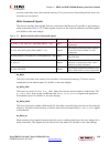
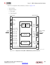
Zynq-7000 ap soc and 7 series fpgas mis v4.1 91 ug586 november 30, 2016 www.Xilinx.Com chapter 1: ddr3 and ddr2 sdram memory interface solution user fpga logic the user fpga logic block shown in figure 1-51 is any fpga design that requires to be connected to an external ddr2 or ddr3 sdram. The user ...
Page 92: User Interface
Zynq-7000 ap soc and 7 series fpgas mis v4.1 92 ug586 november 30, 2016 www.Xilinx.Com chapter 1: ddr3 and ddr2 sdram memory interface solution when a user creates a multicontroller design on their own, each mig output has the component instantiated with the primitive. This violates the rules for id...
Page 93
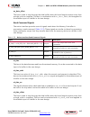
Zynq-7000 ap soc and 7 series fpgas mis v4.1 93 ug586 november 30, 2016 www.Xilinx.Com chapter 1: ddr3 and ddr2 sdram memory interface solution app_addr[addr_width – 1:0] this input indicates the address for the request currently being submitted to the ui. The ui aggregates all the address fields of...
Page 94
Zynq-7000 ap soc and 7 series fpgas mis v4.1 94 ug586 november 30, 2016 www.Xilinx.Com chapter 1: ddr3 and ddr2 sdram memory interface solution app_en this input strobes in a request. You must apply the desired values to app_addr[], app_cmd [2:0], and app_hi_pri, and then assert app_en to submit the...
Page 95
Zynq-7000 ap soc and 7 series fpgas mis v4.1 95 ug586 november 30, 2016 www.Xilinx.Com chapter 1: ddr3 and ddr2 sdram memory interface solution - a write is requested and no write buffer pointers are available ° a periodic read is being inserted app_rd_data[app_data_width – 1:0] this output contains...
Page 96: Axi4 Slave Interface Block
Zynq-7000 ap soc and 7 series fpgas mis v4.1 96 ug586 november 30, 2016 www.Xilinx.Com chapter 1: ddr3 and ddr2 sdram memory interface solution ui_clk_sync_rst this is the reset from the ui which is in synchronous with ui_clk. Ui_clk this is the output clock from the ui. It must be a half or quarter...
Page 97
Zynq-7000 ap soc and 7 series fpgas mis v4.1 97 ug586 november 30, 2016 www.Xilinx.Com chapter 1: ddr3 and ddr2 sdram memory interface solution axi4 slave interface parameters table 1-19 lists the axi4 slave interface parameters. Table 1-19: axi4 slave interface parameters parameter name default val...
Page 98
Zynq-7000 ap soc and 7 series fpgas mis v4.1 98 ug586 november 30, 2016 www.Xilinx.Com chapter 1: ddr3 and ddr2 sdram memory interface solution axi4 slave interface signals table 1-20 lists the axi4 slave interface specific signal. All of the axi interface signals are synchronous to ui_clk. C_s_axi_...
Page 99
Zynq-7000 ap soc and 7 series fpgas mis v4.1 99 ug586 november 30, 2016 www.Xilinx.Com chapter 1: ddr3 and ddr2 sdram memory interface solution s_axi_awready 1 output high write address ready. This signal indicates that the slave is ready to accept an address and associated control signals. S_axi_wd...
Page 100: Arbitration In Axi Shim
Zynq-7000 ap soc and 7 series fpgas mis v4.1 100 ug586 november 30, 2016 www.Xilinx.Com chapter 1: ddr3 and ddr2 sdram memory interface solution arbitration in axi shim the axi4 protocol calls for independent read and write address channels. The memory controller has one address channel. The followi...
Page 101
Zynq-7000 ap soc and 7 series fpgas mis v4.1 101 ug586 november 30, 2016 www.Xilinx.Com chapter 1: ddr3 and ddr2 sdram memory interface solution write priority (write_priority, write_priority_reg) write address channel is always given priority in this mode. The requests from the read address channel...
Page 102
Zynq-7000 ap soc and 7 series fpgas mis v4.1 102 ug586 november 30, 2016 www.Xilinx.Com chapter 1: ddr3 and ddr2 sdram memory interface solution there can be between 0 and c_nck_per_clk × 2 errors per cycle with each data beat signaled by one of the vector bits. Multiple bits of the vector can be si...
Page 103
Zynq-7000 ap soc and 7 series fpgas mis v4.1 103 ug586 november 30, 2016 www.Xilinx.Com chapter 1: ddr3 and ddr2 sdram memory interface solution axi4-lite slave control/status register interface signals table 1-22 lists the axi4 slave interface specific signals. Clock/reset to the interface is provi...
Page 104
Zynq-7000 ap soc and 7 series fpgas mis v4.1 104 ug586 november 30, 2016 www.Xilinx.Com chapter 1: ddr3 and ddr2 sdram memory interface solution axi4-lite slave control/status register map ecc register map is shown in table 1-23 . The register map is little endian. Write accesses to read-only or res...
Page 105
Zynq-7000 ap soc and 7 series fpgas mis v4.1 105 ug586 november 30, 2016 www.Xilinx.Com chapter 1: ddr3 and ddr2 sdram memory interface solution axi4-lite slave control/status register map detailed descriptions ecc_status this register holds information on the occurrence of correctable and uncorrect...
Page 106
Zynq-7000 ap soc and 7 series fpgas mis v4.1 106 ug586 november 30, 2016 www.Xilinx.Com chapter 1: ddr3 and ddr2 sdram memory interface solution ue_en_irq are set to 1 (enabled), the value of the interrupt signal is the logical or between the ce_status and ue_status bits. Ecc_on_off the ecc on/off c...
Page 107
Zynq-7000 ap soc and 7 series fpgas mis v4.1 107 ug586 november 30, 2016 www.Xilinx.Com chapter 1: ddr3 and ddr2 sdram memory interface solution ce_ffa[31:0] this register stores the address (bits[31:0]) of the first occurrence of an access with a correctable error. When the ce_status bit in the ecc...
Page 108
Zynq-7000 ap soc and 7 series fpgas mis v4.1 108 ug586 november 30, 2016 www.Xilinx.Com chapter 1: ddr3 and ddr2 sdram memory interface solution this register is re-enabled to store the data of the next correctable error. Storing of the failing data is enabled after reset. Ce_ffd[95:64] note: this r...
Page 109
Zynq-7000 ap soc and 7 series fpgas mis v4.1 109 ug586 november 30, 2016 www.Xilinx.Com chapter 1: ddr3 and ddr2 sdram memory interface solution table 1-34 describes the register bit usage when dq_width = 72. Table 1-35 describes the register bit usage when dq_width = 144. Ue_ffa[31:0] this register...
Page 110
Zynq-7000 ap soc and 7 series fpgas mis v4.1 110 ug586 november 30, 2016 www.Xilinx.Com chapter 1: ddr3 and ddr2 sdram memory interface solution ue_ffd[31:0] this register stores the (uncorrected) failing data (bits[31:0]) of the first occurrence of an access with an uncorrectable error. When the ue...
Page 111
Zynq-7000 ap soc and 7 series fpgas mis v4.1 111 ug586 november 30, 2016 www.Xilinx.Com chapter 1: ddr3 and ddr2 sdram memory interface solution ue_ffd[127:96] note: this register is only used when the dq_width == 144. This register stores the (uncorrected) failing data (bits[127:96]) of the first o...
Page 112
Zynq-7000 ap soc and 7 series fpgas mis v4.1 112 ug586 november 30, 2016 www.Xilinx.Com chapter 1: ddr3 and ddr2 sdram memory interface solution the register is only implemented if c_ecc_test = “on” or ecc_test_fi_xor = “on” and ecc = “on” in a mig design in the vivado ip catalog. Injecting faults s...
Page 113
Zynq-7000 ap soc and 7 series fpgas mis v4.1 113 ug586 november 30, 2016 www.Xilinx.Com chapter 1: ddr3 and ddr2 sdram memory interface solution injecting faults should be performed in a critical region in software; that is, writing this register and the subsequent write to the memory must not be in...
Page 114: User Interface Block
Zynq-7000 ap soc and 7 series fpgas mis v4.1 114 ug586 november 30, 2016 www.Xilinx.Com chapter 1: ddr3 and ddr2 sdram memory interface solution table 1-48 describes the register bit usage when dq_width = 72. Table 1-49 describes the register bit usage when dq_width = 144. User interface block the u...
Page 115
Zynq-7000 ap soc and 7 series fpgas mis v4.1 115 ug586 november 30, 2016 www.Xilinx.Com chapter 1: ddr3 and ddr2 sdram memory interface solution the bank, row, and column comprise a target address on the memory device for read and write operations. Commands are specified using the cmd[2:0] input to ...
Page 116
Zynq-7000 ap soc and 7 series fpgas mis v4.1 116 ug586 november 30, 2016 www.Xilinx.Com chapter 1: ddr3 and ddr2 sdram memory interface solution receives read data from the external memory. The core echoes this address back when the requests are processed. Write command signals the native interface ...
Page 117
Zynq-7000 ap soc and 7 series fpgas mis v4.1 117 ug586 november 30, 2016 www.Xilinx.Com chapter 1: ddr3 and ddr2 sdram memory interface solution wr_data_offset this bus is used to step through the data buffer when the burst length requires more than a single cycle to complete. This bus, in combinati...
Page 118
Zynq-7000 ap soc and 7 series fpgas mis v4.1 118 ug586 november 30, 2016 www.Xilinx.Com chapter 1: ddr3 and ddr2 sdram memory interface solution native interface maintenance command signals table 1-54 lists the native interface maintenance command signals. App_ref_req when asserted, this active-high...
Page 119: Clocking Architecture
Zynq-7000 ap soc and 7 series fpgas mis v4.1 119 ug586 november 30, 2016 www.Xilinx.Com chapter 1: ddr3 and ddr2 sdram memory interface solution clocking architecture the phy design requires that a pll module be used to generate various clocks, and both global and local clock networks are used to di...
Page 120
Zynq-7000 ap soc and 7 series fpgas mis v4.1 120 ug586 november 30, 2016 www.Xilinx.Com chapter 1: ddr3 and ddr2 sdram memory interface solution • when hr banks are selected for memory interface pins in gui and the memory frequencies ≥ 400 mhz, the phase is 337.5°. • when hr banks are selected for m...
Page 121
Zynq-7000 ap soc and 7 series fpgas mis v4.1 121 ug586 november 30, 2016 www.Xilinx.Com chapter 1: ddr3 and ddr2 sdram memory interface solution write path (output) i/o logic clock the output path comprising both data and controls is clocked by phaser_out. The phaser_out provides synchronized clocks...
Page 122: Memory Controller
Zynq-7000 ap soc and 7 series fpgas mis v4.1 122 ug586 november 30, 2016 www.Xilinx.Com chapter 1: ddr3 and ddr2 sdram memory interface solution memory controller in the core default configuration, the memory controller (mc) resides between the ui block and the physical layer. This is depicted in fi...
Page 123
Zynq-7000 ap soc and 7 series fpgas mis v4.1 123 ug586 november 30, 2016 www.Xilinx.Com chapter 1: ddr3 and ddr2 sdram memory interface solution bank machines most of the memory controller logic resides in the bank machines. Bank machines correspond to dram banks. A given bank machine manages a sing...
Page 124
Zynq-7000 ap soc and 7 series fpgas mis v4.1 124 ug586 november 30, 2016 www.Xilinx.Com chapter 1: ddr3 and ddr2 sdram memory interface solution column commands can be reordered for the purpose of optimizing memory interface throughput. The ordering algorithm nominally ensures data coherence. The re...
Page 125
Zynq-7000 ap soc and 7 series fpgas mis v4.1 125 ug586 november 30, 2016 www.Xilinx.Com chapter 1: ddr3 and ddr2 sdram memory interface solution not all requests require an activate. If a preceding request has activated the same rank, bank, or row, a subsequent request might inherit the bank machine...
Page 126: Error Correcting Code
Zynq-7000 ap soc and 7 series fpgas mis v4.1 126 ug586 november 30, 2016 www.Xilinx.Com chapter 1: ddr3 and ddr2 sdram memory interface solution precharge policy the controller implements an aggressive precharge policy. The controller examines the input queue of requests as each transaction complete...
Page 127
Zynq-7000 ap soc and 7 series fpgas mis v4.1 127 ug586 november 30, 2016 www.Xilinx.Com chapter 1: ddr3 and ddr2 sdram memory interface solution the ecc mode is optional and supported only for a 72-bit data width. The data mask feature is disabled when ecc mode is enabled. When ecc mode is enabled, ...
Page 128
Zynq-7000 ap soc and 7 series fpgas mis v4.1 128 ug586 november 30, 2016 www.Xilinx.Com chapter 1: ddr3 and ddr2 sdram memory interface solution the ecc functionality is implemented as three functional blocks. A write data merge and ecc generate block. A read data ecc decode and correct block and a ...
Page 129
Zynq-7000 ap soc and 7 series fpgas mis v4.1 129 ug586 november 30, 2016 www.Xilinx.Com chapter 1: ddr3 and ddr2 sdram memory interface solution when the wr_bytes command is given, the memory controller performs a read-modify-write (rmw) cycle. When a wr_bytes command is at the head of the queue, it...
Page 130
Zynq-7000 ap soc and 7 series fpgas mis v4.1 130 ug586 november 30, 2016 www.Xilinx.Com chapter 1: ddr3 and ddr2 sdram memory interface solution ecc self-test functionality under normal operating conditions, the ecc part of the data written to the dram array is not visible at the user interface. Thi...
Page 131: Phy
Zynq-7000 ap soc and 7 series fpgas mis v4.1 131 ug586 november 30, 2016 www.Xilinx.Com chapter 1: ddr3 and ddr2 sdram memory interface solution phy the phy provides a physical interface to an external ddr2 or ddr3 sdram. The phy generates the signal timing and sequencing required to interface to th...
Page 132
Zynq-7000 ap soc and 7 series fpgas mis v4.1 132 ug586 november 30, 2016 www.Xilinx.Com chapter 1: ddr3 and ddr2 sdram memory interface solution the memory controller and calibration logic communicate with this dedicated phy in the slow frequency clock domain, which is either a divided by 4 or divid...
Page 133
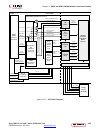
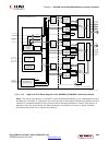
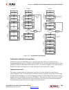
Zynq-7000 ap soc and 7 series fpgas mis v4.1 133 ug586 november 30, 2016 www.Xilinx.Com chapter 1: ddr3 and ddr2 sdram memory interface solution x-ref target - figure 1-56 figure 1-56: phy block diagram )/,/')# )3%2$%3 /3%2$%3 /$$2 )$%,!9 $$2 $$2 3$2!- )/ &)&/s &0'! $$2$$2 &0'! 0(9 #ontrol "lock 0(!...
Page 134
Zynq-7000 ap soc and 7 series fpgas mis v4.1 134 ug586 november 30, 2016 www.Xilinx.Com chapter 1: ddr3 and ddr2 sdram memory interface solution memory initialization and calibration sequence after deassertion of system reset, the phy performs the required power-on initialization sequence for the me...
Page 135
Zynq-7000 ap soc and 7 series fpgas mis v4.1 135 ug586 november 30, 2016 www.Xilinx.Com chapter 1: ddr3 and ddr2 sdram memory interface solution the calibration stages in figure 1-57 correspond to these sections: • memory initialization, page 144 • phaser_in phase lock, page 145 • phaser_in dqsfound...
Page 136
Zynq-7000 ap soc and 7 series fpgas mis v4.1 136 ug586 november 30, 2016 www.Xilinx.Com chapter 1: ddr3 and ddr2 sdram memory interface solution the phy control interface is used by the calibration logic or the memory controller to write phy control words to the phy. The signals in this interface ar...
Page 137
Zynq-7000 ap soc and 7 series fpgas mis v4.1 137 ug586 november 30, 2016 www.Xilinx.Com chapter 1: ddr3 and ddr2 sdram memory interface solution • control offset – this field is used to control when the address and command in/out_fifos are read and transferred to the iois. The control offset is in u...
Page 138
Zynq-7000 ap soc and 7 series fpgas mis v4.1 138 ug586 november 30, 2016 www.Xilinx.Com chapter 1: ddr3 and ddr2 sdram memory interface solution table 1-59: auxiliary output attributes attribute type description mc_ao_wrlvl_en vector[3:0] this attribute specifies whether or not the related aux_outpu...
Page 139
Zynq-7000 ap soc and 7 series fpgas mis v4.1 139 ug586 november 30, 2016 www.Xilinx.Com chapter 1: ddr3 and ddr2 sdram memory interface solution the phy control block has several counters that are not enabled because the synchronous mode is used where phy_clk is either 1/4 or 1/2 the frequency of th...
Page 140
Zynq-7000 ap soc and 7 series fpgas mis v4.1 140 ug586 november 30, 2016 www.Xilinx.Com chapter 1: ddr3 and ddr2 sdram memory interface solution command path a command requested by the calibration logic or memory controller is sent out as a phy control word to the phy control block and a simultaneou...
Page 141
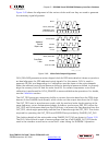
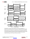
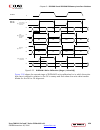
Zynq-7000 ap soc and 7 series fpgas mis v4.1 141 ug586 november 30, 2016 www.Xilinx.Com chapter 1: ddr3 and ddr2 sdram memory interface solution the timing diagram of the address/command path from the output of the out_fifo to the fpga pins is shown in figure 1-59 . X-ref target - figure 1-58 figure...
Page 142
Zynq-7000 ap soc and 7 series fpgas mis v4.1 142 ug586 november 30, 2016 www.Xilinx.Com chapter 1: ddr3 and ddr2 sdram memory interface solution datapath the datapath comprises the write and read datapaths. The datapath in the 7 series fpga is completely implemented in dedicated logic with in/out_fi...
Page 143
Zynq-7000 ap soc and 7 series fpgas mis v4.1 143 ug586 november 30, 2016 www.Xilinx.Com chapter 1: ddr3 and ddr2 sdram memory interface solution each in/out_fifo has a storage array of memory elements arranged as 10 groups eight bits wide and eight entries deep. During a write, the out_fifo receives...
Page 144
Zynq-7000 ap soc and 7 series fpgas mis v4.1 144 ug586 november 30, 2016 www.Xilinx.Com chapter 1: ddr3 and ddr2 sdram memory interface solution the out_fifo serializes from eight bits to four bits and outputs the 4-bit data to the oserdes in the oclkdiv domain that is half the frequency of the ddr2...
Page 145
Zynq-7000 ap soc and 7 series fpgas mis v4.1 145 ug586 november 30, 2016 www.Xilinx.Com chapter 1: ddr3 and ddr2 sdram memory interface solution phaser_in phase lock phaser_in is placed in the read calibration mode to phase align its free-running frequency reference clock to the associated read dqs....
Page 146
Zynq-7000 ap soc and 7 series fpgas mis v4.1 146 ug586 november 30, 2016 www.Xilinx.Com chapter 1: ddr3 and ddr2 sdram memory interface solution each byte group can be read out of the in_fifo on different phy_clk cycles due to fly-by routing and delay differences within each group. Therefore, the in...
Page 147
Zynq-7000 ap soc and 7 series fpgas mis v4.1 147 ug586 november 30, 2016 www.Xilinx.Com chapter 1: ddr3 and ddr2 sdram memory interface solution the timing diagram for write leveling is shown in figure 1-63 . Periodic dqs pulses are output by the fpga memory interface to detect the level of the ck c...
Page 148
Zynq-7000 ap soc and 7 series fpgas mis v4.1 148 ug586 november 30, 2016 www.Xilinx.Com chapter 1: ddr3 and ddr2 sdram memory interface solution implementation details the write_calib_n signal indicating the start of write leveling mode is input to the phy control block after twldqsen to ensure that...
Page 149
Zynq-7000 ap soc and 7 series fpgas mis v4.1 149 ug586 november 30, 2016 www.Xilinx.Com chapter 1: ddr3 and ddr2 sdram memory interface solution multi-purpose register read leveling at this stage of calibration, the write dqs is not centered in the write dq window nor is the read dqs centered in the...
Page 150
Zynq-7000 ap soc and 7 series fpgas mis v4.1 150 ug586 november 30, 2016 www.Xilinx.Com chapter 1: ddr3 and ddr2 sdram memory interface solution • when second edge is not found, second_edge_taps are set to zero. However, the algorithm computes the midpoint of the data window using 63 as the second e...
Page 151
Zynq-7000 ap soc and 7 series fpgas mis v4.1 151 ug586 november 30, 2016 www.Xilinx.Com chapter 1: ddr3 and ddr2 sdram memory interface solution the stage 3 start tap value places the dqs anywhere between 90° and 225° with respect to dq . The number of edges detected depends on the write level taps ...
Page 152
Zynq-7000 ap soc and 7 series fpgas mis v4.1 152 ug586 november 30, 2016 www.Xilinx.Com chapter 1: ddr3 and ddr2 sdram memory interface solution during the centering substage the write dqs is centered in the write dq window based on the edges found during the edge detection stage. At the end of this...
Page 153
Zynq-7000 ap soc and 7 series fpgas mis v4.1 153 ug586 november 30, 2016 www.Xilinx.Com chapter 1: ddr3 and ddr2 sdram memory interface solution figure 1-68 shows an initial dqs to ck alignment case for component interfaces. The assumption is that component interfaces also use the fly-by topology, t...
Page 154
Zynq-7000 ap soc and 7 series fpgas mis v4.1 154 ug586 november 30, 2016 www.Xilinx.Com chapter 1: ddr3 and ddr2 sdram memory interface solution implementation details a write command is issued with a known write data pattern (ff 00 aa 55 55 aa 99 66) to a specific location. This is followed by a re...
Page 155
Zynq-7000 ap soc and 7 series fpgas mis v4.1 155 ug586 november 30, 2016 www.Xilinx.Com chapter 1: ddr3 and ddr2 sdram memory interface solution a phaser_in provides two clock outputs namely iclk and iclkdiv. Iclk is the stage 2 delay output and iclkdiv is the rising edge aligned divided by 2 versio...
Page 156
Zynq-7000 ap soc and 7 series fpgas mis v4.1 156 ug586 november 30, 2016 www.Xilinx.Com chapter 1: ddr3 and ddr2 sdram memory interface solution the first two scenarios would result in the left data window edge being detected with a tap count less than 1/2 the bit time and the second window edge mig...
Page 157
Zynq-7000 ap soc and 7 series fpgas mis v4.1 157 ug586 november 30, 2016 www.Xilinx.Com chapter 1: ddr3 and ddr2 sdram memory interface solution prbs read leveling this stage of read calibration follows the read leveling calibration stage. The dqs phaser_in fine tap setting determined during the rea...
Page 158
Zynq-7000 ap soc and 7 series fpgas mis v4.1 158 ug586 november 30, 2016 www.Xilinx.Com chapter 1: ddr3 and ddr2 sdram memory interface solution important: customers using the phy only design must include the periodic read logic within the custom controller. If the periodic reads are not included, t...
Page 159
Zynq-7000 ap soc and 7 series fpgas mis v4.1 159 ug586 november 30, 2016 www.Xilinx.Com chapter 1: ddr3 and ddr2 sdram memory interface solution the second module, ddr_phy_tempmon, resides in the top-level calibration module, calib_top . It receives the device_temp[11:0] from the tempmon module and ...
Page 160
Zynq-7000 ap soc and 7 series fpgas mis v4.1 160 ug586 november 30, 2016 www.Xilinx.Com chapter 1: ddr3 and ddr2 sdram memory interface solution sync_pulse 1 input – this is the synchronization pulse output by the pll. Pll_lock 1 input – the locked output of the pll instantiated in the infrastructur...
Page 161
Zynq-7000 ap soc and 7 series fpgas mis v4.1 161 ug586 november 30, 2016 www.Xilinx.Com chapter 1: ddr3 and ddr2 sdram memory interface solution mc_cke [nck_per_clk – 1:0] input – mc_cke [nck_per_clk – 1:0] is the cke associated with the dram interface. This signal is valid when the cke_odt_aux para...
Page 162: Designing With The Core
Zynq-7000 ap soc and 7 series fpgas mis v4.1 162 ug586 november 30, 2016 www.Xilinx.Com chapter 1: ddr3 and ddr2 sdram memory interface solution designing with the core the core is bundled with an example design that can be simulated. The example design can be used as a starting point for the user d...
Page 163: Interfacing To The Core
Zynq-7000 ap soc and 7 series fpgas mis v4.1 163 ug586 november 30, 2016 www.Xilinx.Com chapter 1: ddr3 and ddr2 sdram memory interface solution interfacing to the core the memory controller can be connected using either the axi4 slave interface, the ui, or the native interface. The axi4 slave inter...
Page 164: Upsizing
Zynq-7000 ap soc and 7 series fpgas mis v4.1 164 ug586 november 30, 2016 www.Xilinx.Com chapter 1: ddr3 and ddr2 sdram memory interface solution upsizing when the data width on the user interface side is wider than that on the axi interface side, upsizing is performed in the axi shim interface. Data...
Page 165
Zynq-7000 ap soc and 7 series fpgas mis v4.1 165 ug586 november 30, 2016 www.Xilinx.Com chapter 1: ddr3 and ddr2 sdram memory interface solution figure 1-72 and figure 1-73 show that the address map is controlled by the string parameter mem_addr_order. This parameter can take the following values: •...
Page 166
Zynq-7000 ap soc and 7 series fpgas mis v4.1 166 ug586 november 30, 2016 www.Xilinx.Com chapter 1: ddr3 and ddr2 sdram memory interface solution example (2) – when the selected option in the mig gui is row_bank_column and the address to the controller is mapped accordingly. Command path when the use...
Page 167
Zynq-7000 ap soc and 7 series fpgas mis v4.1 167 ug586 november 30, 2016 www.Xilinx.Com chapter 1: ddr3 and ddr2 sdram memory interface solution a non back-to-back write command can be issued as shown in figure 1-75 . This figure depicts three scenarios for the app_wdf_data, app_wdf_wren, and app_wd...
Page 168
Zynq-7000 ap soc and 7 series fpgas mis v4.1 168 ug586 november 30, 2016 www.Xilinx.Com chapter 1: ddr3 and ddr2 sdram memory interface solution write path the write data is registered in the write fifo when app_wdf_wren is asserted and app_wdf_rdy is high ( figure 1-76 ). If app_wdf_rdy is deassert...
Page 169
Zynq-7000 ap soc and 7 series fpgas mis v4.1 169 ug586 november 30, 2016 www.Xilinx.Com chapter 1: ddr3 and ddr2 sdram memory interface solution the data values at different clock edges are as shown in table 1-63 . For a 2:1 memory controller to dram clock ratio, the application data width is 32 bit...
Page 170
Zynq-7000 ap soc and 7 series fpgas mis v4.1 170 ug586 november 30, 2016 www.Xilinx.Com chapter 1: ddr3 and ddr2 sdram memory interface solution read path the read data is returned by the ui in the requested order and is valid when app_rd_data_valid is asserted ( figure 1-81 and figure 1-82 ). The a...
Page 171
Zynq-7000 ap soc and 7 series fpgas mis v4.1 171 ug586 november 30, 2016 www.Xilinx.Com chapter 1: ddr3 and ddr2 sdram memory interface solution a user-refresh operation can be performed any time provided the handshake defined above is followed. There are no additional interfacing requirements with ...
Page 172: Native Interface
Zynq-7000 ap soc and 7 series fpgas mis v4.1 172 ug586 november 30, 2016 www.Xilinx.Com chapter 1: ddr3 and ddr2 sdram memory interface solution to account for the worst case, subtract trcd, cl, the data transit time and trp for each bank machine to ensure that all transactions can complete before t...
Page 173
Zynq-7000 ap soc and 7 series fpgas mis v4.1 173 ug586 november 30, 2016 www.Xilinx.Com chapter 1: ddr3 and ddr2 sdram memory interface solution in figure 1-86 , requests 1 and 2 are accepted normally. The first time request 3 is presented, accept is driven low, and the request is not accepted. The ...
Page 174
Zynq-7000 ap soc and 7 series fpgas mis v4.1 174 ug586 november 30, 2016 www.Xilinx.Com chapter 1: ddr3 and ddr2 sdram memory interface solution transfers can be isolated with gaps of non-activity, or there can be long bursts with no gaps. The user design can identify when a request is being process...
Page 175
Zynq-7000 ap soc and 7 series fpgas mis v4.1 175 ug586 november 30, 2016 www.Xilinx.Com chapter 1: ddr3 and ddr2 sdram memory interface solution a detailed description of the phy architecture and the various stages of calibration are provided in phy, page 131 . The signals required for the memory co...
Page 176
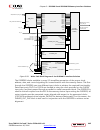
Zynq-7000 ap soc and 7 series fpgas mis v4.1 176 ug586 november 30, 2016 www.Xilinx.Com chapter 1: ddr3 and ddr2 sdram memory interface solution x-ref target - figure 1-88 figure 1-88: phy interface example $$2 3$2!- 0hysical -#?2!3?. -#?#!3?. -#?7%?. -#?#3?. -#?"!;= -#?!$$2%33;= &2%1?2%,+ -#?#-$;= ...
Page 177
Zynq-7000 ap soc and 7 series fpgas mis v4.1 177 ug586 november 30, 2016 www.Xilinx.Com chapter 1: ddr3 and ddr2 sdram memory interface solution the data offset field (mc_data_offset) in the phy control word for read commands is determined during phaser_in dqsfound calibration. It is provided by the...
Page 178
Zynq-7000 ap soc and 7 series fpgas mis v4.1 178 ug586 november 30, 2016 www.Xilinx.Com chapter 1: ddr3 and ddr2 sdram memory interface solution important: bits[31:27, 24:23, 14:12, and 7:3] in table 1-58, page 136 are not used in this example. The write waveform shown in figure 1-90 illustrates an ...
Page 179
Zynq-7000 ap soc and 7 series fpgas mis v4.1 179 ug586 november 30, 2016 www.Xilinx.Com chapter 1: ddr3 and ddr2 sdram memory interface solution important: bits[31:27, 24:23, 14:12, and 7:3] in table 1-58, page 136 are not used in this example. The phy calibration operates with additive latency al) ...
Page 180: Customizing The Core
Zynq-7000 ap soc and 7 series fpgas mis v4.1 180 ug586 november 30, 2016 www.Xilinx.Com chapter 1: ddr3 and ddr2 sdram memory interface solution customizing the core the 7 series fpgas memory interface solution supports several configurations for ddr2 or ddr3 sdram devices. The specific configuratio...
Page 181
Zynq-7000 ap soc and 7 series fpgas mis v4.1 181 ug586 november 30, 2016 www.Xilinx.Com chapter 1: ddr3 and ddr2 sdram memory interface solution ck_width this is the number of ck/ck# outputs to memory. This option is based on the selected mig tool configuration. Cke_width this is the number of cke o...
Page 182
Zynq-7000 ap soc and 7 series fpgas mis v4.1 182 ug586 november 30, 2016 www.Xilinx.Com chapter 1: ddr3 and ddr2 sdram memory interface solution wrlvl this option enables write leveling calibration in ddr3 designs. This parameter must always be “on” for ddr3 and “off” for ddr2. This parameter should...
Page 183
Zynq-7000 ap soc and 7 series fpgas mis v4.1 183 ug586 november 30, 2016 www.Xilinx.Com chapter 1: ddr3 and ddr2 sdram memory interface solution the parameters listed in table 1-65 depend on the selected memory clock frequency, memory device, memory configuration, and fpga speed grade. The values fo...
Page 184
Zynq-7000 ap soc and 7 series fpgas mis v4.1 184 ug586 november 30, 2016 www.Xilinx.Com chapter 1: ddr3 and ddr2 sdram memory interface solution trcd this is the active-to-read or -write command delay. This value, in picoseconds, is based on the device selection in the mig tool. Trefi this is the av...
Page 185
Zynq-7000 ap soc and 7 series fpgas mis v4.1 185 ug586 november 30, 2016 www.Xilinx.Com chapter 1: ddr3 and ddr2 sdram memory interface solution trcd this is the active-to-read or -write command delay. This value, in picoseconds, is based on the device selection in the mig tool. Trefi this is the av...
Page 186
Zynq-7000 ap soc and 7 series fpgas mis v4.1 186 ug586 november 30, 2016 www.Xilinx.Com chapter 1: ddr3 and ddr2 sdram memory interface solution data_io_prim_type this option instantiates ibuf primitives for data (dq) and strobe (dqs) as per banks selected for the interface and also depends on the i...
Page 187
Zynq-7000 ap soc and 7 series fpgas mis v4.1 187 ug586 november 30, 2016 www.Xilinx.Com chapter 1: ddr3 and ddr2 sdram memory interface solution clkout0_phase – phase of pll output clkout0. This value is set by the mig tool based on the banks selected for memory interface pins and the frequency of o...
Page 188
Zynq-7000 ap soc and 7 series fpgas mis v4.1 188 ug586 november 30, 2016 www.Xilinx.Com chapter 1: ddr3 and ddr2 sdram memory interface solution table 1-66 contains parameters set up by the mig tool based on the pinout selected. When making pinout changes, xilinx recommends rerunning the mig tool to...
Page 189
Zynq-7000 ap soc and 7 series fpgas mis v4.1 189 ug586 november 30, 2016 www.Xilinx.Com chapter 1: ddr3 and ddr2 sdram memory interface solution phy_0_bitlanes, phy_1_bitlanes, phy_2_bitlanes 12-bit parameter per byte lane used to determine which i/o locations are used to generate the necessary phy ...
Page 190
Zynq-7000 ap soc and 7 series fpgas mis v4.1 190 ug586 november 30, 2016 www.Xilinx.Com chapter 1: ddr3 and ddr2 sdram memory interface solution addr_map bank and byte lane position information for the address. 12-bit parameter provided per pin. • [11:8] – bank position. Values of 0, 1, or 2 are sup...
Page 191
Zynq-7000 ap soc and 7 series fpgas mis v4.1 191 ug586 november 30, 2016 www.Xilinx.Com chapter 1: ddr3 and ddr2 sdram memory interface solution odt_map bank and byte lane position information for the odt. This parameter is referred to as one of the address/control byte groups. See addr_map descript...
Page 192: Design Guidelines
Zynq-7000 ap soc and 7 series fpgas mis v4.1 192 ug586 november 30, 2016 www.Xilinx.Com chapter 1: ddr3 and ddr2 sdram memory interface solution design guidelines guidelines for ddr2 and ddr3 sdram designs are covered in this section. For general pcb routing guidelines, see appendix a, general memor...
Page 193
Zynq-7000 ap soc and 7 series fpgas mis v4.1 193 ug586 november 30, 2016 www.Xilinx.Com chapter 1: ddr3 and ddr2 sdram memory interface solution bank and pin selection guides for ddr3 designs the mig tool generates pin assignments for a memory interface based on physical layer rules. Xilinx 7 series...
Page 194
Zynq-7000 ap soc and 7 series fpgas mis v4.1 194 ug586 november 30, 2016 www.Xilinx.Com chapter 1: ddr3 and ddr2 sdram memory interface solution ° an unused pin exists in the adjacent byte group (t0/t3) or the ck output is contained in the adjacent byte group. • no more than three vertical banks fro...
Page 195
Zynq-7000 ap soc and 7 series fpgas mis v4.1 195 ug586 november 30, 2016 www.Xilinx.Com chapter 1: ddr3 and ddr2 sdram memory interface solution through the frequency backbone to the pll. The system clock input to the pll must come from clock capable i/o. The system clock input can only be used for ...
Page 196
Zynq-7000 ap soc and 7 series fpgas mis v4.1 196 ug586 november 30, 2016 www.Xilinx.Com chapter 1: ddr3 and ddr2 sdram memory interface solution power system and plane discontinuities see 7 series fpgas pcb design and pin planning guide (ug483) [ref 12] . Termination these rules apply to termination...
Page 197
Zynq-7000 ap soc and 7 series fpgas mis v4.1 197 ug586 november 30, 2016 www.Xilinx.Com chapter 1: ddr3 and ddr2 sdram memory interface solution • differential signals should be terminated with the memory device internal termination or an 80Ω differential termination at the load ( figure 1-93 ). For...
Page 198
Zynq-7000 ap soc and 7 series fpgas mis v4.1 198 ug586 november 30, 2016 www.Xilinx.Com chapter 1: ddr3 and ddr2 sdram memory interface solution • dci (hp banks) or in_term (hr banks) is required at the fpga to meet the specified performance. • the reset_n signal is not terminated. This signal shoul...
Page 199
Zynq-7000 ap soc and 7 series fpgas mis v4.1 199 ug586 november 30, 2016 www.Xilinx.Com chapter 1: ddr3 and ddr2 sdram memory interface solution • the maximum electrical delay between any address and control signals and the corresponding ck/ck# must be ≤ ±25 ps, with 8 ps being the optimal target. •...
Page 200
Zynq-7000 ap soc and 7 series fpgas mis v4.1 200 ug586 november 30, 2016 www.Xilinx.Com chapter 1: ddr3 and ddr2 sdram memory interface solution for example, if an 1,866 rated –3 fpga operates at 1,600 mb/s with a 1,600 rated ddr3 component, the dq to dqs skew limit is ±31.3 ps. If the interface ope...
Page 201
Zynq-7000 ap soc and 7 series fpgas mis v4.1 201 ug586 november 30, 2016 www.Xilinx.Com chapter 1: ddr3 and ddr2 sdram memory interface solution for example, if an 1,863 mb/s rated fpga operates at 1600 mb/s with a 1,600 rated ddr3 component, the ck to address/control skew limit is ±94.1 ps. If a 1,...
Page 202
Zynq-7000 ap soc and 7 series fpgas mis v4.1 202 ug586 november 30, 2016 www.Xilinx.Com chapter 1: ddr3 and ddr2 sdram memory interface solution • sys_rst – this is the main system reset (asynchronous). The reset signal must be applied for a minimum pulse width of 5 ns. • init_calib_complete – this ...
Page 203: Ddr2 Sdram
Zynq-7000 ap soc and 7 series fpgas mis v4.1 203 ug586 november 30, 2016 www.Xilinx.Com chapter 1: ddr3 and ddr2 sdram memory interface solution consult the constraints guide for more information. For ddr3 sdram interfaces that have the memory system input clock (sys_clk_p/sys_clk_n) placed on ccio ...
Page 204
Zynq-7000 ap soc and 7 series fpgas mis v4.1 204 ug586 november 30, 2016 www.Xilinx.Com chapter 1: ddr3 and ddr2 sdram memory interface solution associated i/os. In a typical ddr2 configuration, eight of these 10 i/os are used for the dqs: one is used for the data mask (dm), and one remains for othe...
Page 205
Zynq-7000 ap soc and 7 series fpgas mis v4.1 205 ug586 november 30, 2016 www.Xilinx.Com chapter 1: ddr3 and ddr2 sdram memory interface solution • for data widths of 16 with a x8 part, only one set of ck/ck#, cs, odt ports is generated to fit the design in a single bank. • vrn and vrp are used for t...
Page 206
Zynq-7000 ap soc and 7 series fpgas mis v4.1 206 ug586 november 30, 2016 www.Xilinx.Com chapter 1: ddr3 and ddr2 sdram memory interface solution system clock, pll location, and constraints the pll is required to be in the bank that supplies the clock to the memory to meet the specified interface per...
Page 207
Zynq-7000 ap soc and 7 series fpgas mis v4.1 207 ug586 november 30, 2016 www.Xilinx.Com chapter 1: ddr3 and ddr2 sdram memory interface solution these signals are all set to lvcmos25 and can be altered as needed for the system design. They can be generated and used internally instead of being brough...
Page 208
Zynq-7000 ap soc and 7 series fpgas mis v4.1 208 ug586 november 30, 2016 www.Xilinx.Com chapter 1: ddr3 and ddr2 sdram memory interface solution source can be connected directly to the diff_sstl18_ii ccio pins. For more details on usage and required circuitry for lvds and lvds_25 i/o standards, see ...
Page 209
Zynq-7000 ap soc and 7 series fpgas mis v4.1 209 ug586 november 30, 2016 www.Xilinx.Com chapter 1: ddr3 and ddr2 sdram memory interface solution • dm should be pulled to gnd if odt is used but dm is not driven by the fpga (for scenarios where the data mask is not used or is disabled). I/o standards ...
Page 210: Clocking
Zynq-7000 ap soc and 7 series fpgas mis v4.1 210 ug586 november 30, 2016 www.Xilinx.Com chapter 1: ddr3 and ddr2 sdram memory interface solution these rules indicate the maximum electrical delays between ddr2 sdram signals: • the maximum electrical delay between any dq or dm and its associated dqs/d...
Page 211
Zynq-7000 ap soc and 7 series fpgas mis v4.1 211 ug586 november 30, 2016 www.Xilinx.Com chapter 1: ddr3 and ddr2 sdram memory interface solution • the clock input (sys_clk) can be input on any ccio in the column where the memory interface is located; this includes ccio in banks that do not contain t...
Page 212
Zynq-7000 ap soc and 7 series fpgas mis v4.1 212 ug586 november 30, 2016 www.Xilinx.Com chapter 1: ddr3 and ddr2 sdram memory interface solution provides the 100Ω differential receiver termination because the internal diff_term is set to false. To maximize the input noise margin, all rbias resistors...
Page 213: Ddr3 Pinout Examples
Zynq-7000 ap soc and 7 series fpgas mis v4.1 213 ug586 november 30, 2016 www.Xilinx.Com chapter 1: ddr3 and ddr2 sdram memory interface solution information on sharing bufg clock (phy_clk) the mig 7 series ddr3 design includes an mmcm which outputs the phy_clk on a bufg route. It is not possible to ...
Page 214
Zynq-7000 ap soc and 7 series fpgas mis v4.1 214 ug586 november 30, 2016 www.Xilinx.Com chapter 1: ddr3 and ddr2 sdram memory interface solution 1 dqs1_n d_06 n 43 dqs-n 1 dq11 d_05 p 42 – 1 dq10 d_04 n 41 – 1 dq9 d_03 p 40 – 1 dq8 d_02 n 39 – 1 dm1 d_01 p 38 – 1 – d_00 n 37 – 1 dq7 c_11 p 36 – 1 dq...
Page 215
Zynq-7000 ap soc and 7 series fpgas mis v4.1 215 ug586 november 30, 2016 www.Xilinx.Com chapter 1: ddr3 and ddr2 sdram memory interface solution table 1-70 shows an example of a 32-bit ddr3 interface contained within two banks. This example uses 2 gb x8 components. 1 a8 a_08 n 9 – 1 a7 a_07 p 8 dqs-...
Page 216
Zynq-7000 ap soc and 7 series fpgas mis v4.1 216 ug586 november 30, 2016 www.Xilinx.Com chapter 1: ddr3 and ddr2 sdram memory interface solution 1 – c_06 n 31 dqs-n 1 – c_05 p 30 – 1 – c_04 n 29 – 1 – c_03 p 28 ccio-p 1 – c_02 n 27 ccio-n 1 cke c_01 p 26 ccio-p 1 odt c_00 n 25 ccio-n 1 ras_n b_11 p ...
Page 217
Zynq-7000 ap soc and 7 series fpgas mis v4.1 217 ug586 november 30, 2016 www.Xilinx.Com chapter 1: ddr3 and ddr2 sdram memory interface solution 2 dq30 d_10 n 47 – 2 dq29 d_09 p 46 – 2 dq28 d_08 n 45 – 2 dqs3_p d_07 p 44 dqs-p 2 dqs3_n d_06 n 43 dqs-n 2 dq27 d_05 p 42 – 2 dq26 d_04 n 41 – 2 dq25 d_0...
Page 218
Zynq-7000 ap soc and 7 series fpgas mis v4.1 218 ug586 november 30, 2016 www.Xilinx.Com chapter 1: ddr3 and ddr2 sdram memory interface solution table 1-71 shows an example of a 64-bit ddr3 interface contained within three banks. This example uses four 2 gb x16 components. 2 – b_00 n 13 – 2 dq7 a_11...
Page 219
Zynq-7000 ap soc and 7 series fpgas mis v4.1 219 ug586 november 30, 2016 www.Xilinx.Com chapter 1: ddr3 and ddr2 sdram memory interface solution 1 dq54 c_10 n 35 – 1 dq53 c_09 p 34 – 1 dq52 c_08 n 33 – 1 dqs6_p c_07 p 32 dqs-p 1 dqs6_n c_06 n 31 dqs-n 1 dq51 c_05 p 30 – 1 dq50 c_04 n 29 – 1 dq49 c_0...
Page 220
Zynq-7000 ap soc and 7 series fpgas mis v4.1 220 ug586 november 30, 2016 www.Xilinx.Com chapter 1: ddr3 and ddr2 sdram memory interface solution 1 – a_00 n 1 – 1 vrn – se 0 – 2 vrp – se 49 – 2 – d_11 p 48 – 2 – d_10 n 47 – 2 – d_09 p 46 – 2 – d_08 n 45 – 2 – d_07 p 44 dqs-p 2 – d_06 n 43 dqs-n 2 – d...
Page 221
Zynq-7000 ap soc and 7 series fpgas mis v4.1 221 ug586 november 30, 2016 www.Xilinx.Com chapter 1: ddr3 and ddr2 sdram memory interface solution 2 ba0 b_04 n 17 – 2 cs_n b_03 p 16 – 2 cke b_02 n 15 – 2 a13 b_01 p 14 – 2 a12 b_00 n 13 – 2 a11 a_11 p 12 – 2 a10 a_10 n 11 – 2 a9 a_09 p 10 – 2 a8 a_08 n...
Page 222
Zynq-7000 ap soc and 7 series fpgas mis v4.1 222 ug586 november 30, 2016 www.Xilinx.Com chapter 1: ddr3 and ddr2 sdram memory interface solution 3 dq20 c_08 n 33 – 3 dqs2_p c_07 p 32 dqs-p 3 dqs2_n c_06 n 31 dqs-n 3 dq19 c_05 p 30 – 3 dq18 c_04 n 29 – 3 dq17 c_03 p 28 ccio-p 3 dq16 c_02 n 27 ccio-n ...
Page 223
Zynq-7000 ap soc and 7 series fpgas mis v4.1 223 ug586 november 30, 2016 www.Xilinx.Com chapter 1: ddr3 and ddr2 sdram memory interface solution table 1-72 shows an example of a 72-bit ddr3 interface contained within three banks. This example is for a 4 gb udimm using nine 4 gb x8 components. The se...
Page 224
Zynq-7000 ap soc and 7 series fpgas mis v4.1 224 ug586 november 30, 2016 www.Xilinx.Com chapter 1: ddr3 and ddr2 sdram memory interface solution 1 dqs5_p b_07 p 20 dqs-p 1 dqs5_n b_06 n 19 dqs-n 1 dq43 b_05 p 18 – 1 dq42 b_04 n 17 – 1 dq41 b_03 p 16 – 1 dq40 b_02 n 15 – 1 dm5 b_01 p 14 – 1 – b_00 n ...
Page 225
Zynq-7000 ap soc and 7 series fpgas mis v4.1 225 ug586 november 30, 2016 www.Xilinx.Com chapter 1: ddr3 and ddr2 sdram memory interface solution 2 – c_11 p 36 – 2 – c_10 n 35 – 2 – c_09 p 34 – 2 – c_08 n 33 – 2 – c_07 p 32 dqs-p 2 – c_06 n 31 dqs-n 2 – c_05 p 30 – 2 – c_04 n 29 – 2 – c_03 p 28 ccio-...
Page 226
Zynq-7000 ap soc and 7 series fpgas mis v4.1 226 ug586 november 30, 2016 www.Xilinx.Com chapter 1: ddr3 and ddr2 sdram memory interface solution 2 a1 a_01 p 2 – 2 a0 a_00 n 1 – 2 vrn – se 0 – 3 vrp – se 49 – 3 dq31 d_11 p 48 – 3 dq30 d_10 n 47 – 3 dq29 d_09 p 46 – 3 dq28 d_08 n 45 – 3 dqs3_p d_07 p ...
Page 227
Zynq-7000 ap soc and 7 series fpgas mis v4.1 227 ug586 november 30, 2016 www.Xilinx.Com chapter 1: ddr3 and ddr2 sdram memory interface solution 3 dq11 b_05 p 18 – 3 dq10 b_04 n 17 – 3 dq9 b_03 p 16 – 3 dq8 b_02 n 15 – 3 dm1 b_01 p 14 – 3 – b_00 n 13 – 3 dq7 a_11 p 12 – 3 dq6 a_10 n 11 – 3 dq5 a_09 ...
Page 228: Debugging Ddr3/ddr2 Designs
Zynq-7000 ap soc and 7 series fpgas mis v4.1 228 ug586 november 30, 2016 www.Xilinx.Com chapter 1: ddr3 and ddr2 sdram memory interface solution debugging ddr3/ddr2 designs calibration failures and data errors can occur for many reasons and the debug of these errors can be time consuming. This secti...
Page 229: Debug Tools
Zynq-7000 ap soc and 7 series fpgas mis v4.1 229 ug586 november 30, 2016 www.Xilinx.Com chapter 1: ddr3 and ddr2 sdram memory interface solution answer records for this core can also be located by using the search support box on the main xilinx support web page . To maximize your search results, use...
Page 230
Zynq-7000 ap soc and 7 series fpgas mis v4.1 230 ug586 november 30, 2016 www.Xilinx.Com chapter 1: ddr3 and ddr2 sdram memory interface solution debug signals the mig 7 series tool includes a debug signals control option on the fpga options screen. Enabling this feature allows calibration, tap delay...
Page 231: Hardware Debug
Zynq-7000 ap soc and 7 series fpgas mis v4.1 231 ug586 november 30, 2016 www.Xilinx.Com chapter 1: ddr3 and ddr2 sdram memory interface solution reference boards various xilinx development boards support mig ip core that include fpga interfaces to a ddr sodimm. These boards can be used to prototype ...
Page 232
Zynq-7000 ap soc and 7 series fpgas mis v4.1 232 ug586 november 30, 2016 www.Xilinx.Com chapter 1: ddr3 and ddr2 sdram memory interface solution many of these common issues can also be applied to debugging design simulations. Details are provided on: • general checks • calibration stages • determine...
Page 233
Zynq-7000 ap soc and 7 series fpgas mis v4.1 233 ug586 november 30, 2016 www.Xilinx.Com chapter 1: ddr3 and ddr2 sdram memory interface solution • check the reset to ensure the polarity is correct and the signal is clean. The reset signal must be applied for a minimum pulse width of 5 ns. • check te...
Page 234
Zynq-7000 ap soc and 7 series fpgas mis v4.1 234 ug586 november 30, 2016 www.Xilinx.Com chapter 1: ddr3 and ddr2 sdram memory interface solution calibration stages memory initialization the phy executes a jedec-compliant ddr2 or ddr3 initialization sequence following the deassertion of system reset....
Page 235
Zynq-7000 ap soc and 7 series fpgas mis v4.1 235 ug586 november 30, 2016 www.Xilinx.Com chapter 1: ddr3 and ddr2 sdram memory interface solution determine the failing calibration stage using the vivado logic analyzer feature, configure the device along with debug_nets.Ltx file. This file can be foun...
Page 236
Zynq-7000 ap soc and 7 series fpgas mis v4.1 236 ug586 november 30, 2016 www.Xilinx.Com chapter 1: ddr3 and ddr2 sdram memory interface solution debug signals table 1-74: ddr2/ddr3 debug signals signal name description ila signals (status) dbg_init_calib_complete signifies memory initialization and ...
Page 237
Zynq-7000 ap soc and 7 series fpgas mis v4.1 237 ug586 november 30, 2016 www.Xilinx.Com chapter 1: ddr3 and ddr2 sdram memory interface solution dbg_rddata_r read data read out of the in_fifo for the dqs group selected through dbg_dqs on the vio. This is a 64-bit bus. This debug port does not captur...
Page 238
Zynq-7000 ap soc and 7 series fpgas mis v4.1 238 ug586 november 30, 2016 www.Xilinx.Com chapter 1: ddr3 and ddr2 sdram memory interface solution dbg_wl_po_fine_cnt_by_dqs phaser_out fine taps found during write leveling. Byte capture based on vio dbg_dqs setting. Dbg_wl_po_coarse_cnt_by_dqs phaser_o...
Page 239
Zynq-7000 ap soc and 7 series fpgas mis v4.1 239 ug586 november 30, 2016 www.Xilinx.Com chapter 1: ddr3 and ddr2 sdram memory interface solution dbg_pi_phase_locked_phy4lanes signifies which of the phaser_in lanes has achieved lock. It is a 12-bit bus, three nibble data. Each nibble corresponds to a...
Page 240
Zynq-7000 ap soc and 7 series fpgas mis v4.1 240 ug586 november 30, 2016 www.Xilinx.Com chapter 1: ddr3 and ddr2 sdram memory interface solution dbg_mux_rd_valid_r asserts when the valid pattern is detected on dbg_mux_rd_rise0_r, dbg_mux_rd_fall0_r, dbg_mux_rd_rise1_r, dbg_mux_rd_fall1_r, dbg_mux_rd...
Page 241
Zynq-7000 ap soc and 7 series fpgas mis v4.1 241 ug586 november 30, 2016 www.Xilinx.Com chapter 1: ddr3 and ddr2 sdram memory interface solution dbg_wcal_mux_rd_rise0_r data pattern received on the write calibration stage mux on rising edge 0. Dbg_wcal_mux_rd_fall0_r data pattern received on the wri...
Page 242
Zynq-7000 ap soc and 7 series fpgas mis v4.1 242 ug586 november 30, 2016 www.Xilinx.Com chapter 1: ddr3 and ddr2 sdram memory interface solution vio_instr_mode_value see table 1-83 . Vio_bl_mode_value see table 1-83 . Vio_fixed_bl_value see table 1-83 . Vio_data_mask_gen enables traffic generator da...
Page 243
Zynq-7000 ap soc and 7 series fpgas mis v4.1 243 ug586 november 30, 2016 www.Xilinx.Com chapter 1: ddr3 and ddr2 sdram memory interface solution debugging phaser_in phaselocked calibration failures (dbg_pi_phaselock_err = 1) calibration overview during this stage of calibration, each phaser_in is pl...
Page 244
Zynq-7000 ap soc and 7 series fpgas mis v4.1 244 ug586 november 30, 2016 www.Xilinx.Com chapter 1: ddr3 and ddr2 sdram memory interface solution debug • if the dqsfound stage fails, probe dqs at the memory. Sets of four back-to-back reads should be seen. Read dqs(s) is required by the phaser_in(s) t...
Page 245
Zynq-7000 ap soc and 7 series fpgas mis v4.1 245 ug586 november 30, 2016 www.Xilinx.Com chapter 1: ddr3 and ddr2 sdram memory interface solution look at dbg_rd_data_offset, dbg_calib_rd_data_offest_1, and dbg_calib_rd_data_offest _2 , these values should vary by one at the most. Next, compare these ...
Page 246
Zynq-7000 ap soc and 7 series fpgas mis v4.1 246 ug586 november 30, 2016 www.Xilinx.Com chapter 1: ddr3 and ddr2 sdram memory interface solution expected vivado logic analyzer tool results debugging write leveling failures (dbg_wrlvl_err = 1) calibration overview write leveling, a new feature in ddr...
Page 247
Zynq-7000 ap soc and 7 series fpgas mis v4.1 247 ug586 november 30, 2016 www.Xilinx.Com chapter 1: ddr3 and ddr2 sdram memory interface solution debug • verify dqs is toggling on the board. The fpga sends dqs during write leveling. If dqs is not toggling, something is wrong with the setup and the ge...
Page 248
Zynq-7000 ap soc and 7 series fpgas mis v4.1 248 ug586 november 30, 2016 www.Xilinx.Com chapter 1: ddr3 and ddr2 sdram memory interface solution note: the tap variance across dqs byte groups is quite different due to fly-by routing. Expected vivado logic analyzer tool results table 1-76: debug signa...
Page 249
Zynq-7000 ap soc and 7 series fpgas mis v4.1 249 ug586 november 30, 2016 www.Xilinx.Com chapter 1: ddr3 and ddr2 sdram memory interface solution debugging mpr read leveling failures – ddr3 only (dbg_rdlvl_err[1] = 1) calibration overview at this stage of calibration, the write dqs is not centered in...
Page 250
Zynq-7000 ap soc and 7 series fpgas mis v4.1 250 ug586 november 30, 2016 www.Xilinx.Com chapter 1: ddr3 and ddr2 sdram memory interface solution debug • if this stage of calibration failed with the assertion of dbg_rdlvl_err[1], set the ila trigger to dbg_rdlvl_err[1]. • if this stage of calibration...
Page 251
Zynq-7000 ap soc and 7 series fpgas mis v4.1 251 ug586 november 30, 2016 www.Xilinx.Com chapter 1: ddr3 and ddr2 sdram memory interface solution the mig design only looks at dq[0]. If there is an issue with dq[0], the mpr calibration stage would fail. • if a dqs byte group failed this stage of calib...
Page 252
Zynq-7000 ap soc and 7 series fpgas mis v4.1 252 ug586 november 30, 2016 www.Xilinx.Com chapter 1: ddr3 and ddr2 sdram memory interface solution debugging oclkdelayed calibration failures calibration overview the 7 series mmcm has outputs with "fine phase shift" capability. This fine phase shift cap...
Page 253
Zynq-7000 ap soc and 7 series fpgas mis v4.1 253 ug586 november 30, 2016 www.Xilinx.Com chapter 1: ddr3 and ddr2 sdram memory interface solution debugging write calibration failures (dbg_wrcal_err = 1) calibration overview write calibration is required to align dqs to the correct ck edge. During wri...
Page 254
Zynq-7000 ap soc and 7 series fpgas mis v4.1 254 ug586 november 30, 2016 www.Xilinx.Com chapter 1: ddr3 and ddr2 sdram memory interface solution • two ck early write pattern read back – 55aa9966bb11ee44 • one ck late write pattern read back – xxxxff00aa5555aa ° calibration cannot correct for this pa...
Page 255
Zynq-7000 ap soc and 7 series fpgas mis v4.1 255 ug586 november 30, 2016 www.Xilinx.Com chapter 1: ddr3 and ddr2 sdram memory interface solution 1. The number on wrcal_dqs_cnt when dbg_wrcal_err asserts signifies the byte that failed write calibration. Debug should be focused on this byte group. 2. ...
Page 256
Zynq-7000 ap soc and 7 series fpgas mis v4.1 256 ug586 november 30, 2016 www.Xilinx.Com chapter 1: ddr3 and ddr2 sdram memory interface solution c. Using high quality scope and probes, verify the expected pattern (ff00aa5555aa9966) is being written to the dram during a write and that the expected pa...
Page 257
Zynq-7000 ap soc and 7 series fpgas mis v4.1 257 ug586 november 30, 2016 www.Xilinx.Com chapter 1: ddr3 and ddr2 sdram memory interface solution expected vivado logic analyzer tool results x-ref target - figure 1-103 figure 1-103: trigger = dbg_wrcal_done send feedback.
Page 258
Zynq-7000 ap soc and 7 series fpgas mis v4.1 258 ug586 november 30, 2016 www.Xilinx.Com chapter 1: ddr3 and ddr2 sdram memory interface solution debugging read leveling failures (dbg_rdlvl_err[0] = 1) for memory clock frequencies of 400 mhz and above, read leveling is performed after write calibrati...
Page 259
Zynq-7000 ap soc and 7 series fpgas mis v4.1 259 ug586 november 30, 2016 www.Xilinx.Com chapter 1: ddr3 and ddr2 sdram memory interface solution • if this stage of calibration was successful and the results need to be analyzed, set the ila trigger to dbg_rdlvl_done[0] = r. • set the vio dbg_dqs for ...
Page 260
Zynq-7000 ap soc and 7 series fpgas mis v4.1 260 ug586 november 30, 2016 www.Xilinx.Com chapter 1: ddr3 and ddr2 sdram memory interface solution • look at how many edges (up to two) were found. Less than two edges can be found when running around or below 400 mhz. Otherwise, two edges should always ...
Page 261
Zynq-7000 ap soc and 7 series fpgas mis v4.1 261 ug586 november 30, 2016 www.Xilinx.Com chapter 1: ddr3 and ddr2 sdram memory interface solution debugging prbs read leveling failures calibration overview this stage of calibration was added in mig 7 series v1.7 and determines the read data valid wind...
Page 262
Zynq-7000 ap soc and 7 series fpgas mis v4.1 262 ug586 november 30, 2016 www.Xilinx.Com chapter 1: ddr3 and ddr2 sdram memory interface solution ref_bit signifies that reference bit of the byte which has largest left edge phaser_in tap value. Complex_victim_inc indicates the victim increment for int...
Page 263
Zynq-7000 ap soc and 7 series fpgas mis v4.1 263 ug586 november 30, 2016 www.Xilinx.Com chapter 1: ddr3 and ddr2 sdram memory interface solution calibration times for initial es (ies) with extended calibration, completing calibration in hardware should take about 30 seconds. For general es (ges) and...
Page 264
Zynq-7000 ap soc and 7 series fpgas mis v4.1 264 ug586 november 30, 2016 www.Xilinx.Com chapter 1: ddr3 and ddr2 sdram memory interface solution table 1-83: debug signals used for configuring the traffic generator signal name description vio_modify_enable set to 1 to vary the command traffic generat...
Page 265
Zynq-7000 ap soc and 7 series fpgas mis v4.1 265 ug586 november 30, 2016 www.Xilinx.Com chapter 1: ddr3 and ddr2 sdram memory interface solution vio_data_mode_value valid settings for this signal are: • 0x0 = reserved • 0x1 = fixed – 32 bits of fixed_data as defined through fixed_data_i inputs. (1) ...
Page 266
Zynq-7000 ap soc and 7 series fpgas mis v4.1 266 ug586 november 30, 2016 www.Xilinx.Com chapter 1: ddr3 and ddr2 sdram memory interface solution isolating the data error using either the mig 7 series traffic generator or the user design, the first step in data error debug is to isolate when and wher...
Page 267
Zynq-7000 ap soc and 7 series fpgas mis v4.1 267 ug586 november 30, 2016 www.Xilinx.Com chapter 1: ddr3 and ddr2 sdram memory interface solution b. Observe the dbg_rddata_r and cmp_data_r signals in vivado logic analyzer feature. - are errors seen on a data bit/s belonging to a certain dqs group(s)?...
Page 268
Zynq-7000 ap soc and 7 series fpgas mis v4.1 268 ug586 november 30, 2016 www.Xilinx.Com chapter 1: ddr3 and ddr2 sdram memory interface solution determining if a data error is due to the write or read determining whether a data error is due to the write or the read can be difficult because if writes...
Page 269
Zynq-7000 ap soc and 7 series fpgas mis v4.1 269 ug586 november 30, 2016 www.Xilinx.Com chapter 1: ddr3 and ddr2 sdram memory interface solution vio_fixed_instr_value = 1 (read only) vio_pause_traffic = 0 5. Observe the dbg_rddata_r and cmp_data_r signals in vivado logic analyzer feature. This can a...
Page 270
Zynq-7000 ap soc and 7 series fpgas mis v4.1 270 ug586 november 30, 2016 www.Xilinx.Com chapter 1: ddr3 and ddr2 sdram memory interface solution • check the idelay values after calibration. Look for variations between idelay values. Idelay values should be very similar for dqs in the same dqs group....
Page 271
Zynq-7000 ap soc and 7 series fpgas mis v4.1 271 ug586 november 30, 2016 www.Xilinx.Com chapter 1: ddr3 and ddr2 sdram memory interface solution win_byte_select can be used to select between each byte groups measured results and display them to the vivado logic analyzer feature waveform window. To c...
Page 272: Interface Debug
Zynq-7000 ap soc and 7 series fpgas mis v4.1 272 ug586 november 30, 2016 www.Xilinx.Com chapter 1: ddr3 and ddr2 sdram memory interface solution interface debug axi4-lite interfaces the axi4 slave interface follows the axi4 memory-mapped slave protocol specification as described in the arm amba open...
Page 273
Zynq-7000 ap soc and 7 series fpgas mis v4.1 273 ug586 november 30, 2016 www.Xilinx.Com chapter 1: ddr3 and ddr2 sdram memory interface solution clock_dedicated_route constraints system clock if the srcc/mrcc i/o pin and pll are not allocated in the same bank, the clock_dedicated_route constraint mu...
Page 274: Introduction
Zynq-7000 ap soc and 7 series fpgas mis v4.1 274 ug586 november 30, 2016 www.Xilinx.Com chapter 2 qdr ii+ memory interface solution introduction the qdr ii+ sram memory interface solution (mis) is a physical layer for interfacing xilinx ® 7 series fpgas user designs to qdr ii+ sram devices. Qdr ii+ ...
Page 275
Zynq-7000 ap soc and 7 series fpgas mis v4.1 275 ug586 november 30, 2016 www.Xilinx.Com chapter 2: qdr ii+ memory interface solution important: memory interface solutions v4.1 only supports the vivado ® design suite. The ise ® design suite is not supported in this version. Using mig in the vivado de...
Page 276
Zynq-7000 ap soc and 7 series fpgas mis v4.1 276 ug586 november 30, 2016 www.Xilinx.Com chapter 2: qdr ii+ memory interface solution 3. Click next to proceed to the project name page ( figure 2-3 ). Enter the project name and project location. Based on the details provided, the project is saved in t...
Page 277
Zynq-7000 ap soc and 7 series fpgas mis v4.1 277 ug586 november 30, 2016 www.Xilinx.Com chapter 2: qdr ii+ memory interface solution 4. Click next to proceed to the project type page ( figure 2-4 ). Select the project type as rtl project because mig deliverables are rtl files. X-ref target - figure ...
Page 278
Zynq-7000 ap soc and 7 series fpgas mis v4.1 278 ug586 november 30, 2016 www.Xilinx.Com chapter 2: qdr ii+ memory interface solution 5. Click next to proceed to the add sources page ( figure 2-5 ). Rtl files can be added to the project in this page. If the project was not created earlier, proceed to...
Page 279
Zynq-7000 ap soc and 7 series fpgas mis v4.1 279 ug586 november 30, 2016 www.Xilinx.Com chapter 2: qdr ii+ memory interface solution 6. Click next to open the add existing ip (optional) page ( figure 2-6 ). If the ip is already created, the xci file generated by the ip can be added to the project an...
Page 280
Zynq-7000 ap soc and 7 series fpgas mis v4.1 280 ug586 november 30, 2016 www.Xilinx.Com chapter 2: qdr ii+ memory interface solution 7. Click next to open the add constraints (optional) page ( figure 2-7 ). If the constraints file exists in the repository, it can be added to the project. Proceed to ...
Page 281
Zynq-7000 ap soc and 7 series fpgas mis v4.1 281 ug586 november 30, 2016 www.Xilinx.Com chapter 2: qdr ii+ memory interface solution 8. Click next to proceed to the default part page ( figure 2-8 ) where the device that needs to be targeted can be selected. The default part page appears as shown in ...
Page 282
Zynq-7000 ap soc and 7 series fpgas mis v4.1 282 ug586 november 30, 2016 www.Xilinx.Com chapter 2: qdr ii+ memory interface solution select the target family, package,and speed grade. The valid devices are displayed in the same page, and the device can be selected based on the targeted device ( figu...
Page 283
Zynq-7000 ap soc and 7 series fpgas mis v4.1 283 ug586 november 30, 2016 www.Xilinx.Com chapter 2: qdr ii+ memory interface solution 9. Click next to open the new project summary page ( figure 2-11 ). This includes the summary of selected project details. 10. Click finish to complete the project cre...
Page 284
Zynq-7000 ap soc and 7 series fpgas mis v4.1 284 ug586 november 30, 2016 www.Xilinx.Com chapter 2: qdr ii+ memory interface solution 11. Click ip catalog on the project manager window to open the vivado ip catalog window. The ip catalog window appears on the right side panel (see figure 2-12 , highl...
Page 285
Zynq-7000 ap soc and 7 series fpgas mis v4.1 285 ug586 november 30, 2016 www.Xilinx.Com chapter 2: qdr ii+ memory interface solution 14. Click next to display the output options page. Customizing and generating the core caution! The windows operating system has a 260-character limit for path lengths...
Page 286
Zynq-7000 ap soc and 7 series fpgas mis v4.1 286 ug586 november 30, 2016 www.Xilinx.Com chapter 2: qdr ii+ memory interface solution mig outputs are generated with the folder name . Important: only alphanumeric characters can be used for . Special characters cannot be used. This name should always s...
Page 287
Zynq-7000 ap soc and 7 series fpgas mis v4.1 287 ug586 november 30, 2016 www.Xilinx.Com chapter 2: qdr ii+ memory interface solution 1. Select any of the compatible fpgas in the list. Only the common pins between the target and selected fpgas are used by the mig tool. The name in the text box signif...
Page 288
Zynq-7000 ap soc and 7 series fpgas mis v4.1 288 ug586 november 30, 2016 www.Xilinx.Com chapter 2: qdr ii+ memory interface solution qdr ii+ sram designs do not support memory-mapped axi4 interfaces. X-ref target - figure 2-16 figure 2-16: memory selection page send feedback.
Page 289
Zynq-7000 ap soc and 7 series fpgas mis v4.1 289 ug586 november 30, 2016 www.Xilinx.Com chapter 2: qdr ii+ memory interface solution controller options this page shows the various controller options that can be selected. • frequency – this feature indicates the operating frequency for all the contro...
Page 290
Zynq-7000 ap soc and 7 series fpgas mis v4.1 290 ug586 november 30, 2016 www.Xilinx.Com chapter 2: qdr ii+ memory interface solution • latency mode – if fixed latency through the core is needed, the fixed latency mode option allows you to select the desired latency. This option can be used if the us...
Page 291
Zynq-7000 ap soc and 7 series fpgas mis v4.1 291 ug586 november 30, 2016 www.Xilinx.Com chapter 2: qdr ii+ memory interface solution the create custom part page includes all of the specifications of the memory component selected in the select base part pull-down menu. 1. Enter the appropriate memory...
Page 292
Zynq-7000 ap soc and 7 series fpgas mis v4.1 292 ug586 november 30, 2016 www.Xilinx.Com chapter 2: qdr ii+ memory interface solution • input clock period – the desired input clock period is selected from the list. These values are determined by the chosen memory clock period and the allowable limits...
Page 293
Zynq-7000 ap soc and 7 series fpgas mis v4.1 293 ug586 november 30, 2016 www.Xilinx.Com chapter 2: qdr ii+ memory interface solution • reference clock – this option selects the clock type (single-ended, differential, no buffer, or use system clock) for the clk_ref signal pair. The use system clock o...
Page 294
Zynq-7000 ap soc and 7 series fpgas mis v4.1 294 ug586 november 30, 2016 www.Xilinx.Com chapter 2: qdr ii+ memory interface solution extended fpga options figure 2-22 shows the extended fpga options page. • digitally controlled impedance (dci) – when selected, this option internally terminates the s...
Page 295
Zynq-7000 ap soc and 7 series fpgas mis v4.1 295 ug586 november 30, 2016 www.Xilinx.Com chapter 2: qdr ii+ memory interface solution i/o planning options figure 2-23 shows the i/o planning options page. • pin/bank selection mode – this allows you to specify an existing pinout and generate the rtl fo...
Page 296
Zynq-7000 ap soc and 7 series fpgas mis v4.1 296 ug586 november 30, 2016 www.Xilinx.Com chapter 2: qdr ii+ memory interface solution bank selection this feature allows the selection of bytes for the memory interface. Bytes can be selected for different classes of memory signals, such as: • address a...
Page 297
Zynq-7000 ap soc and 7 series fpgas mis v4.1 297 ug586 november 30, 2016 www.Xilinx.Com chapter 2: qdr ii+ memory interface solution x-ref target - figure 2-25 figure 2-25: bank selection page send feedback.
Page 298
Zynq-7000 ap soc and 7 series fpgas mis v4.1 298 ug586 november 30, 2016 www.Xilinx.Com chapter 2: qdr ii+ memory interface solution system pins selection select the pins for the system signals on this page. The mig tool allows the selection of either external pins or internal connections, as desire...
Page 299
Zynq-7000 ap soc and 7 series fpgas mis v4.1 299 ug586 november 30, 2016 www.Xilinx.Com chapter 2: qdr ii+ memory interface solution • sys_rst – this is the asynchronous system reset input that can be generated internally or driven from a pin. The mig tool selects an appropriate i/o standard for the...
Page 300
Zynq-7000 ap soc and 7 series fpgas mis v4.1 300 ug586 november 30, 2016 www.Xilinx.Com chapter 2: qdr ii+ memory interface solution click next to move to the pcb information page. Pcb information this page displays the pcb-related information to be considered while designing the board that uses the...
Page 301
Zynq-7000 ap soc and 7 series fpgas mis v4.1 301 ug586 november 30, 2016 www.Xilinx.Com chapter 2: qdr ii+ memory interface solution vivado integrated design flow for mig 1. After clicking generate, the generate output products window appears. This window has the out-of-context settings as shown in ...
Page 302
Zynq-7000 ap soc and 7 series fpgas mis v4.1 302 ug586 november 30, 2016 www.Xilinx.Com chapter 2: qdr ii+ memory interface solution 2. Click out-of-context settings to configure generation of synthesized checkpoints. To enable the out-of-context flow, enable the check box. To disable the out-of-con...
Page 303
Zynq-7000 ap soc and 7 series fpgas mis v4.1 303 ug586 november 30, 2016 www.Xilinx.Com chapter 2: qdr ii+ memory interface solution 4. After generating the mig design, the project window appears as shown in figure 2-30 . 5. After project creation, the xci file is added to the project hierarchy. The...
Page 304
Zynq-7000 ap soc and 7 series fpgas mis v4.1 304 ug586 november 30, 2016 www.Xilinx.Com chapter 2: qdr ii+ memory interface solution design generation from mig can be generated using the create design flow or the verify pin changes and update design flows. There is no difference between the flow whe...
Page 305
Zynq-7000 ap soc and 7 series fpgas mis v4.1 305 ug586 november 30, 2016 www.Xilinx.Com chapter 2: qdr ii+ memory interface solution 7. Clicking the generate output products option brings up the manage outputs window ( figure 2-33 ). X-ref target - figure 2-32 figure 2-32: generate rtl and constrain...
Page 306
Zynq-7000 ap soc and 7 series fpgas mis v4.1 306 ug586 november 30, 2016 www.Xilinx.Com chapter 2: qdr ii+ memory interface solution 8. All user-design rtl and constraints files (xdc files) can be viewed in the sources > libraries tab ( figure 2-34 ). 9. The vivado design suite supports the open ip ...
Page 307
Zynq-7000 ap soc and 7 series fpgas mis v4.1 307 ug586 november 30, 2016 www.Xilinx.Com chapter 2: qdr ii+ memory interface solution 10. This option creates a new vivado project. Selecting the menu brings up a dialog box, which guides you to the directory for a new design project. Select a directory...
Page 308
Zynq-7000 ap soc and 7 series fpgas mis v4.1 308 ug586 november 30, 2016 www.Xilinx.Com chapter 2: qdr ii+ memory interface solution 11. Click generate bitstream under project manager > program and debug to generate the bit file for the generated design. The /.Runs/ impl_1 directory includes all rep...
Page 309
Zynq-7000 ap soc and 7 series fpgas mis v4.1 309 ug586 november 30, 2016 www.Xilinx.Com chapter 2: qdr ii+ memory interface solution directory structure and file descriptions this section explains the mig tool directory structure and provides detailed output file descriptions. Output directory struc...
Page 310
Zynq-7000 ap soc and 7 series fpgas mis v4.1 310 ug586 november 30, 2016 www.Xilinx.Com chapter 2: qdr ii+ memory interface solution mig_7series_v4_1 docs example_design par rtl traffic_gen sim synth user_design rtl clocking controller ip_top phy ui xdc directory and file contents the 7 series fpgas...
Page 311
Zynq-7000 ap soc and 7 series fpgas mis v4.1 311 ug586 november 30, 2016 www.Xilinx.Com chapter 2: qdr ii+ memory interface solution table 2-2 lists the files in the example_design/rtl/traffic_gen directory. Table 2-2: files in example_design/rtl/traffic_gen directory name (1) description memc_traff...
Page 312
Zynq-7000 ap soc and 7 series fpgas mis v4.1 312 ug586 november 30, 2016 www.Xilinx.Com chapter 2: qdr ii+ memory interface solution table 2-3 lists the files in the example_design/sim directory. /user_design the user_design folder contains the following: • rtl and xdc folders • top-level wrapper mo...
Page 313
Zynq-7000 ap soc and 7 series fpgas mis v4.1 313 ug586 november 30, 2016 www.Xilinx.Com chapter 2: qdr ii+ memory interface solution user_design/rtl/phy table 2-5 lists the files in the user_design/rtl/phy directory: table 2-4: files in user_design/rtl/clocking directory name (1) description infrast...
Page 314
Zynq-7000 ap soc and 7 series fpgas mis v4.1 314 ug586 november 30, 2016 www.Xilinx.Com chapter 2: qdr ii+ memory interface solution /user_design/xdc table 2-6 lists the files in the user_design/xdc directory. Verify pin changes and update design this feature verifies the input xdc for bank selectio...
Page 315
Zynq-7000 ap soc and 7 series fpgas mis v4.1 315 ug586 november 30, 2016 www.Xilinx.Com chapter 2: qdr ii+ memory interface solution ° interface banks should reside in the same column of the fpga. ° interface banks should be either high performance (hp) or high range (hr). Hp banks are used for the ...
Page 316
Zynq-7000 ap soc and 7 series fpgas mis v4.1 316 ug586 november 30, 2016 www.Xilinx.Com chapter 2: qdr ii+ memory interface solution • verified system pin rules: ° system clock: - these pins should be allocated to either sr/mr cc i/o pair. - these pins must be allocated in the memory banks column. -...
Page 317: Core Architecture
Zynq-7000 ap soc and 7 series fpgas mis v4.1 317 ug586 november 30, 2016 www.Xilinx.Com chapter 2: qdr ii+ memory interface solution core architecture overview figure 2-38 shows a high-level block diagram of the 7 series fpga qdr ii+ sram interface solution. This figure shows both the internal fpga ...
Page 318
Zynq-7000 ap soc and 7 series fpgas mis v4.1 318 ug586 november 30, 2016 www.Xilinx.Com chapter 2: qdr ii+ memory interface solution the phy is composed of these elements, as shown in figure 2-39 : • user interface • physical interface a. Write path b. Read datapath x-ref target - figure 2-39 figure...
Page 319: User Interface
Zynq-7000 ap soc and 7 series fpgas mis v4.1 319 ug586 november 30, 2016 www.Xilinx.Com chapter 2: qdr ii+ memory interface solution the client interface (also known as the user interface) uses a protocol based entirely on single data rate (sdr) signals to make read and write requests. For more deta...
Page 320
Zynq-7000 ap soc and 7 series fpgas mis v4.1 320 ug586 november 30, 2016 www.Xilinx.Com chapter 2: qdr ii+ memory interface solution app_rd_cmd1 input read command. This signal is used to issue a read request and indicates that the address on port 1 is valid. App_rd_data1[data_width × 2 – 1:0] outpu...
Page 321
Zynq-7000 ap soc and 7 series fpgas mis v4.1 321 ug586 november 30, 2016 www.Xilinx.Com chapter 2: qdr ii+ memory interface solution interfacing with the core through the client interface the client interface protocol is the same for using the port 0 or port 1 interface signals and is shown in figur...
Page 322: Clocking Architecture
Zynq-7000 ap soc and 7 series fpgas mis v4.1 322 ug586 november 30, 2016 www.Xilinx.Com chapter 2: qdr ii+ memory interface solution clocking architecture the phy design requires that a pll module be used to generate various clocks. Both global and local clock networks are used to distribute the clo...
Page 323
Zynq-7000 ap soc and 7 series fpgas mis v4.1 323 ug586 november 30, 2016 www.Xilinx.Com chapter 2: qdr ii+ memory interface solution figure 2-41 shows the clocking architecture. The default setting for the pll multiply (m) and divide (d) values is for the system clock input frequency to be equal to ...
Page 324: Physical Interface
Zynq-7000 ap soc and 7 series fpgas mis v4.1 324 ug586 november 30, 2016 www.Xilinx.Com chapter 2: qdr ii+ memory interface solution table 2-8 lists the signals used in the infrastructure module that provides the necessary clocks and reset signals required in the design. Physical interface the physi...
Page 325
Zynq-7000 ap soc and 7 series fpgas mis v4.1 325 ug586 november 30, 2016 www.Xilinx.Com chapter 2: qdr ii+ memory interface solution interfacing with the memory device figure 2-42 shows the physical interface protocol for a four-word memory device. In four-word burst mode: • the address is in sdr fo...
Page 326
Zynq-7000 ap soc and 7 series fpgas mis v4.1 326 ug586 november 30, 2016 www.Xilinx.Com chapter 2: qdr ii+ memory interface solution • phaser_in/phaser_out blocks are available in each byte group and are multi-stage programmable delay line loops that can provide precision phase adjustment of the clo...
Page 327: Write Path
Zynq-7000 ap soc and 7 series fpgas mis v4.1 327 ug586 november 30, 2016 www.Xilinx.Com chapter 2: qdr ii+ memory interface solution write path the write path to the qdr ii+ sram includes the address, data, and control signals necessary to execute a write operation. The address signals in four-word ...
Page 328
Zynq-7000 ap soc and 7 series fpgas mis v4.1 328 ug586 november 30, 2016 www.Xilinx.Com chapter 2: qdr ii+ memory interface solution x-ref target - figure 2-44 figure 2-44: write path /54?&)&/ $;= 234 72#,+ 2$#,+ 2$%. &5,, $;= $;= $;= $;= $;= $;= $;= $;= $;= &2% 1"" 72%. 1;= 1;= 1;= 1;= 1;= 1;= 1;= ...
Page 329: Output Path
Zynq-7000 ap soc and 7 series fpgas mis v4.1 329 ug586 november 30, 2016 www.Xilinx.Com chapter 2: qdr ii+ memory interface solution the clocking details of the address/control using phaser_out are shown in figure 2-45 . Output path because the address/command and write data are provided by the user...
Page 330
Zynq-7000 ap soc and 7 series fpgas mis v4.1 330 ug586 november 30, 2016 www.Xilinx.Com chapter 2: qdr ii+ memory interface solution phy control block the qdr phy uses the phy control block to interface to the out_fifos and phaser_out_phy. The phy control block helps to prevent the condition where o...
Page 331
Zynq-7000 ap soc and 7 series fpgas mis v4.1 331 ug586 november 30, 2016 www.Xilinx.Com chapter 2: qdr ii+ memory interface solution the delay counter is used to delay the phy control block from fetching the next command from the phy control word fifo, and allows time for it to be filled to capacity...
Page 332: Read Path
Zynq-7000 ap soc and 7 series fpgas mis v4.1 332 ug586 november 30, 2016 www.Xilinx.Com chapter 2: qdr ii+ memory interface solution the oserdes is used to clock all outputs from the phy to the memory device. Upon exiting the oserdes, all the output signals must be presented center aligned with resp...
Page 333: Calibration
Zynq-7000 ap soc and 7 series fpgas mis v4.1 333 ug586 november 30, 2016 www.Xilinx.Com chapter 2: qdr ii+ memory interface solution calibration the calibration logic provides the required amount of delay on the read clock and read data to align the clock in the center of the data valid window. The ...
Page 334
Zynq-7000 ap soc and 7 series fpgas mis v4.1 334 ug586 november 30, 2016 www.Xilinx.Com chapter 2: qdr ii+ memory interface solution calibration of read clock and data the phaser_in/phaser_out clocks within each byte group are used to clock all iserdes used to capture read data (q) associated with t...
Page 335
Zynq-7000 ap soc and 7 series fpgas mis v4.1 335 ug586 november 30, 2016 www.Xilinx.Com chapter 2: qdr ii+ memory interface solution data alignment and valid generation this phase of calibration: • ensures read data from all the read byte groups are aligned to the rising edge of the iserdes clkdiv c...
Page 336: Write Calibration
Zynq-7000 ap soc and 7 series fpgas mis v4.1 336 ug586 november 30, 2016 www.Xilinx.Com chapter 2: qdr ii+ memory interface solution write calibration when a write calibration is enabled for design that has memory frequency runs at 400 mhz or above, the results of read calibration data alignment are...
Page 337: Customizing The Core
Zynq-7000 ap soc and 7 series fpgas mis v4.1 337 ug586 november 30, 2016 www.Xilinx.Com chapter 2: qdr ii+ memory interface solution customizing the core the 7 series fpgas qdr ii+ sram interface solution is customizable to support several configurations. The specific configuration is defined by ver...
Page 338
Zynq-7000 ap soc and 7 series fpgas mis v4.1 338 ug586 november 30, 2016 www.Xilinx.Com chapter 2: qdr ii+ memory interface solution sysclk_type this parameter indicates whether the system uses single-ended system clocks, differential system clocks, or is driven from an internal clock (no buffer). B...
Page 339
Zynq-7000 ap soc and 7 series fpgas mis v4.1 339 ug586 november 30, 2016 www.Xilinx.Com chapter 2: qdr ii+ memory interface solution table 2-13 contains parameters set up by the mig tool based on the pinout selected. When making pinout changes, xilinx recommends rerunning the mig tool to set up the ...
Page 340
Zynq-7000 ap soc and 7 series fpgas mis v4.1 340 ug586 november 30, 2016 www.Xilinx.Com chapter 2: qdr ii+ memory interface solution data_ctl_b0, data_ctl_b1, data_ctl_b2 defines mode of use of byte lanes in a given i/o bank. A 1 in a bit position indicates a byte lane is used for data, and a 0 indi...
Page 341
Zynq-7000 ap soc and 7 series fpgas mis v4.1 341 ug586 november 30, 2016 www.Xilinx.Com chapter 2: qdr ii+ memory interface solution cq_map bank and byte lane position information for the read clocks (cq/cq#). See the k_map description. This parameter varies based on the pinout and should not be cha...
Page 342: Design Guidelines
Zynq-7000 ap soc and 7 series fpgas mis v4.1 342 ug586 november 30, 2016 www.Xilinx.Com chapter 2: qdr ii+ memory interface solution design guidelines design rules memory types, memory parts, and data widths are restricted based on the selected fpga, fpga speed grade, and the design frequency. The f...
Page 343: Trace Length Requirements
Zynq-7000 ap soc and 7 series fpgas mis v4.1 343 ug586 november 30, 2016 www.Xilinx.Com chapter 2: qdr ii+ memory interface solution bank sharing among controllers no unused part of a bank used in a memory interface is permitted to be shared with another memory interface. The dedicated logic that co...
Page 344: Pinout Requirements
Zynq-7000 ap soc and 7 series fpgas mis v4.1 344 ug586 november 30, 2016 www.Xilinx.Com chapter 2: qdr ii+ memory interface solution • the maximum electrical delay between any address and control signals and the corresponding k/k# should be ± 50 ps. • there is no relation between cq and the k clocks...
Page 345: Configuration
Zynq-7000 ap soc and 7 series fpgas mis v4.1 345 ug586 november 30, 2016 www.Xilinx.Com chapter 2: qdr ii+ memory interface solution • xilinx recommends keeping the system clock pins in the data write bank. Recommended: although the mig allows system clock selection to be in different super logic re...
Page 346
Zynq-7000 ap soc and 7 series fpgas mis v4.1 346 ug586 november 30, 2016 www.Xilinx.Com chapter 2: qdr ii+ memory interface solution • sys_rst – this signal is the main system reset (asynchronous). • init_calib_complete – this signal indicates when the internal calibration is done and that the inter...
Page 347: Termination
Zynq-7000 ap soc and 7 series fpgas mis v4.1 347 ug586 november 30, 2016 www.Xilinx.Com chapter 2: qdr ii+ memory interface solution for qdr ii+ sram interfaces that have the memory system input clock (sys_clk_p/sys_clk_n) placed on ccio pins within one of the memory banks, mig assigns the diff_hstl...
Page 348: Clocking
Zynq-7000 ap soc and 7 series fpgas mis v4.1 348 ug586 november 30, 2016 www.Xilinx.Com chapter 2: qdr ii+ memory interface solution dci (hp banks) or in_term (hr banks) is required at the fpga to meet the specified performance. Designs generated by the mig tool use the dci standards for data read (...
Page 349
Zynq-7000 ap soc and 7 series fpgas mis v4.1 349 ug586 november 30, 2016 www.Xilinx.Com chapter 2: qdr ii+ memory interface solution ° the above settings must ensure the minimum pll vco frequency (fvcomin) is met. For specifications, see the appropriate dc and switching characteristics data sheet. T...
Page 350
Zynq-7000 ap soc and 7 series fpgas mis v4.1 350 ug586 november 30, 2016 www.Xilinx.Com chapter 2: qdr ii+ memory interface solution c. The differential signals at the input pins meet the vidiff (min) requirements in the corresponding lvds or lvds_25 dc specifications tables of the specific device f...
Page 351: Introduction
Zynq-7000 ap soc and 7 series fpgas mis v4.1 351 ug586 november 30, 2016 www.Xilinx.Com chapter 2: qdr ii+ memory interface solution the sys_clk can be input on any ccio in the column where the memory interfaces are located. This includes ccio in banks that do not contain the memory interfaces, but ...
Page 352: Debug Tools
Zynq-7000 ap soc and 7 series fpgas mis v4.1 352 ug586 november 30, 2016 www.Xilinx.Com chapter 2: qdr ii+ memory interface solution this section defines a step-by-step debugging procedure to assist in the identification and resolution of any issues that might arise during each phase of the design p...
Page 353: Simulation Debug
Zynq-7000 ap soc and 7 series fpgas mis v4.1 353 ug586 november 30, 2016 www.Xilinx.Com chapter 2: qdr ii+ memory interface solution debug signals the mig tool includes a debug signals control option on the fpga options screen. Enabling this feature allows calibration, tap delay, and read data signa...
Page 354
Zynq-7000 ap soc and 7 series fpgas mis v4.1 354 ug586 november 30, 2016 www.Xilinx.Com chapter 2: qdr ii+ memory interface solution verifying the simulation using the example design the example design generated by the mig tool includes a simulation test bench and parameter file based on memory sele...
Page 355
Zynq-7000 ap soc and 7 series fpgas mis v4.1 355 ug586 november 30, 2016 www.Xilinx.Com chapter 2: qdr ii+ memory interface solution 2. Under the simulation tab as shown in figure 2-50 , set the xsim.Simulate.Runtime as 1 ms (there are simulation rtl directives which stop the simulation after certai...
Page 356
Zynq-7000 ap soc and 7 series fpgas mis v4.1 356 ug586 november 30, 2016 www.Xilinx.Com chapter 2: qdr ii+ memory interface solution 3. In the flow navigator window, select run simulation and select run behavioral simulation as shown in figure 2-51 . Simulation flow using questa advanced simulator 1...
Page 357
Zynq-7000 ap soc and 7 series fpgas mis v4.1 357 ug586 november 30, 2016 www.Xilinx.Com chapter 2: qdr ii+ memory interface solution 4. In the flow navigator window, select run simulation and select run behavioral simulation as shown in figure 2-51 . 5. Vivado invokes questa advanced simulator and s...
Page 358
Zynq-7000 ap soc and 7 series fpgas mis v4.1 358 ug586 november 30, 2016 www.Xilinx.Com chapter 2: qdr ii+ memory interface solution a. Browse to the compiled libraries location and set the path on compiles libraries location option. B. Under the compilation tab, set the vcs.Compile.Vlogan.More_opti...
Page 359
Zynq-7000 ap soc and 7 series fpgas mis v4.1 359 ug586 november 30, 2016 www.Xilinx.Com chapter 2: qdr ii+ memory interface solution 5. Vivado invokes vcs and simulations are run in the vcs tool. For more information, see the vivado design suite user guide: logic simulation (ug900) [ref 8] . Simulat...
Page 360
Zynq-7000 ap soc and 7 series fpgas mis v4.1 360 ug586 november 30, 2016 www.Xilinx.Com chapter 2: qdr ii+ memory interface solution 3. Apply the settings and select ok. 4. In the flow navigator window, select run simulation and select run behavioral simulation as shown in figure 2-51 . 5. Vivado in...
Page 361
Zynq-7000 ap soc and 7 series fpgas mis v4.1 361 ug586 november 30, 2016 www.Xilinx.Com chapter 2: qdr ii+ memory interface solution for detailed information on setting up xilinx libraries, see compxlib in the command line tools user guide (ug628) [ref 17] and the synthesis and simulation design gui...
Page 362
Zynq-7000 ap soc and 7 series fpgas mis v4.1 362 ug586 november 30, 2016 www.Xilinx.Com chapter 2: qdr ii+ memory interface solution calibration calibration completes read leveling, write calibration, and read enable calibration. This is completed over two stages. This sequence successfully complete...
Page 363
Zynq-7000 ap soc and 7 series fpgas mis v4.1 363 ug586 november 30, 2016 www.Xilinx.Com chapter 2: qdr ii+ memory interface solution the second stage performs a read enable calibration. The data pattern used during this stage is ..55..Aa. The data pattern is first written to the memory, and then rea...
Page 364
Zynq-7000 ap soc and 7 series fpgas mis v4.1 364 ug586 november 30, 2016 www.Xilinx.Com chapter 2: qdr ii+ memory interface solution proper write and read commands when sending write and read commands, you must properly assert and deassert the corresponding ui inputs. See user interface, page 319 an...
Page 365
Zynq-7000 ap soc and 7 series fpgas mis v4.1 365 ug586 november 30, 2016 www.Xilinx.Com chapter 2: qdr ii+ memory interface solution synthesis and implementation debug figure 2-62 shows the debug flow for synthesis and implementation. Important: the standard synthesis flow for synplify is not suppor...
Page 366: Hardware Debug
Zynq-7000 ap soc and 7 series fpgas mis v4.1 366 ug586 november 30, 2016 www.Xilinx.Com chapter 2: qdr ii+ memory interface solution any timing violations that are encountered must be isolated. The timing report output by trace (.Twx/.Twr) should be analyzed to determine if the failing paths exist i...
Page 367
Zynq-7000 ap soc and 7 series fpgas mis v4.1 367 ug586 november 30, 2016 www.Xilinx.Com chapter 2: qdr ii+ memory interface solution verify board pinout you should ensure that the pinout provided by the mig tool is used without modification. Then, the board schematic should be compared to the .Pad r...
Page 368: Debugging The Core
Zynq-7000 ap soc and 7 series fpgas mis v4.1 368 ug586 november 30, 2016 www.Xilinx.Com chapter 2: qdr ii+ memory interface solution isolating bit errors an important hardware debug step is to try to isolate when and where the bit errors occur. Looking at the bit errors, these should be identified: ...
Page 369
Zynq-7000 ap soc and 7 series fpgas mis v4.1 369 ug586 november 30, 2016 www.Xilinx.Com chapter 2: qdr ii+ memory interface solution when running the core in hardware, a few key signals should be inspected to determine the status of the design. The dbg_phy_status bus described in table 2-16 consists...
Page 370
Zynq-7000 ap soc and 7 series fpgas mis v4.1 370 ug586 november 30, 2016 www.Xilinx.Com chapter 2: qdr ii+ memory interface solution margin check debug signals are provided to move either clocks or data to verify functionality and to confirm sufficient margin is available for reliable operation. The...
Page 371
Zynq-7000 ap soc and 7 series fpgas mis v4.1 371 ug586 november 30, 2016 www.Xilinx.Com chapter 2: qdr ii+ memory interface solution 10. Decrement the phaser_in taps using dbg_pi_f_dec to find the other edge of the window until another error occurs ( tg_compare_error should be asserted). 11. Record ...
Page 372
Zynq-7000 ap soc and 7 series fpgas mis v4.1 372 ug586 november 30, 2016 www.Xilinx.Com chapter 2: qdr ii+ memory interface solution 3. The current bit and byte being measured are indicated by the vio signals dbg_win_current_bit and dbg_win_current_byte, respectively. 4. To get the left and right ta...
Page 373
Zynq-7000 ap soc and 7 series fpgas mis v4.1 373 ug586 november 30, 2016 www.Xilinx.Com chapter 2: qdr ii+ memory interface solution table 2-18: debug_port signal descriptions signal direction description dbg_phy_wr_cmd_n[1:0] output this active-low signal is the internal wr_cmd used for debug with ...
Page 374
Zynq-7000 ap soc and 7 series fpgas mis v4.1 374 ug586 november 30, 2016 www.Xilinx.Com chapter 2: qdr ii+ memory interface solution write init debug signals table 2-19 indicates the mapping between the write init debug signals on the dbg_wr_init bus and debug signals in the phy. All signals are fou...
Page 375
Zynq-7000 ap soc and 7 series fpgas mis v4.1 375 ug586 november 30, 2016 www.Xilinx.Com chapter 2: qdr ii+ memory interface solution read stage 1 calibration debug signals table 2-20 indicates the mapping between bits within the dbg_rd_stage1_cal bus and debug signals in the phy. All signals are fou...
Page 376
Zynq-7000 ap soc and 7 series fpgas mis v4.1 376 ug586 november 30, 2016 www.Xilinx.Com chapter 2: qdr ii+ memory interface solution read stage 2 calibration debug table 2-21 indicates the mapping between bits within the dbg_rd_stage2_cal bus and debug signals in the phy. All signals are found withi...
Page 377
Zynq-7000 ap soc and 7 series fpgas mis v4.1 377 ug586 november 30, 2016 www.Xilinx.Com chapter 2: qdr ii+ memory interface solution dbg_stage2_cal[10] edge_adv_cal_start indicates start of edge_adv calibration, to see if the pi_edge_adv signal needs to be asserted dbg_stage2_cal[11] rd0_vld indicat...
Page 378
Zynq-7000 ap soc and 7 series fpgas mis v4.1 378 ug586 november 30, 2016 www.Xilinx.Com chapter 2: qdr ii+ memory interface solution clock_dedicated_route constraints system clock if the srcc/mrcc i/o pin and pll are not allocated in the same bank, the clock_dedicated_route constraint must be set to...
Page 379: Introduction
Zynq-7000 ap soc and 7 series fpgas mis v4.1 379 ug586 november 30, 2016 www.Xilinx.Com chapter 3 rldram ii and rldram 3 memory interface solutions introduction the rldram ii and rldram 3 memory interface solutions (mis) are a memory controller and physical layer for interfacing xilinx ® 7 series fp...
Page 380
Zynq-7000 ap soc and 7 series fpgas mis v4.1 380 ug586 november 30, 2016 www.Xilinx.Com chapter 3: rldram ii and rldram 3 memory interface solutions using mig in the vivado design suite this section provides the steps to generate the memory interface generator (mig) ip core using the vivado design s...
Page 381
Zynq-7000 ap soc and 7 series fpgas mis v4.1 381 ug586 november 30, 2016 www.Xilinx.Com chapter 3: rldram ii and rldram 3 memory interface solutions 3. Click next to proceed to the project name page ( figure 3-3 ). Enter the project name and project location. Based on the details provided, the proje...
Page 382
Zynq-7000 ap soc and 7 series fpgas mis v4.1 382 ug586 november 30, 2016 www.Xilinx.Com chapter 3: rldram ii and rldram 3 memory interface solutions 4. Click next to proceed to the project type page ( figure 3-4 ). Select the project type as rtl project because mig deliverables are rtl files. 5. Cli...
Page 383
Zynq-7000 ap soc and 7 series fpgas mis v4.1 383 ug586 november 30, 2016 www.Xilinx.Com chapter 3: rldram ii and rldram 3 memory interface solutions 6. Click next to open the add existing ip (optional) page ( figure 3-6 ). If the ip is already created, the xci file generated by the ip can be added t...
Page 384
Zynq-7000 ap soc and 7 series fpgas mis v4.1 384 ug586 november 30, 2016 www.Xilinx.Com chapter 3: rldram ii and rldram 3 memory interface solutions 8. Click next to proceed to the default part page ( figure 3-8 ) where the device that needs to be targeted can be selected. The default part page appe...
Page 385
Zynq-7000 ap soc and 7 series fpgas mis v4.1 385 ug586 november 30, 2016 www.Xilinx.Com chapter 3: rldram ii and rldram 3 memory interface solutions select the target family, package, and speed grade. The valid devices are displayed in the same page, and the device can be selected based on the targe...
Page 386
Zynq-7000 ap soc and 7 series fpgas mis v4.1 386 ug586 november 30, 2016 www.Xilinx.Com chapter 3: rldram ii and rldram 3 memory interface solutions 9. Click next to open the new project summary page ( figure 3-11 ). This includes the summary of selected project details. 10. Click finish to complete...
Page 387
Zynq-7000 ap soc and 7 series fpgas mis v4.1 387 ug586 november 30, 2016 www.Xilinx.Com chapter 3: rldram ii and rldram 3 memory interface solutions 11. Click ip catalog on the project manager window to open the vivado ip catalog window. The ip catalog window appears on the right side panel (see fig...
Page 388
Zynq-7000 ap soc and 7 series fpgas mis v4.1 388 ug586 november 30, 2016 www.Xilinx.Com chapter 3: rldram ii and rldram 3 memory interface solutions 13. Select mig 7 series to open the mig tool ( figure 3-13 ). 14. Click next to display the output options page. Customizing and generating the core ca...
Page 389
Zynq-7000 ap soc and 7 series fpgas mis v4.1 389 ug586 november 30, 2016 www.Xilinx.Com chapter 3: rldram ii and rldram 3 memory interface solutions mig outputs are generated with the folder name . Important: only alphanumeric characters can be used for . Special characters cannot be used. This name...
Page 390
Zynq-7000 ap soc and 7 series fpgas mis v4.1 390 ug586 november 30, 2016 www.Xilinx.Com chapter 3: rldram ii and rldram 3 memory interface solutions 1. Select any of the compatible fpgas in the list. Only the common pins between the target and selected fpgas are used by the mig tool. The name in the...
Page 391
Zynq-7000 ap soc and 7 series fpgas mis v4.1 391 ug586 november 30, 2016 www.Xilinx.Com chapter 3: rldram ii and rldram 3 memory interface solutions rldram ii and rldram 3 designs currently do not support memory-mapped axi4 interfaces. X-ref target - figure 3-16 figure 3-16: memory selection page se...
Page 392
Zynq-7000 ap soc and 7 series fpgas mis v4.1 392 ug586 november 30, 2016 www.Xilinx.Com chapter 3: rldram ii and rldram 3 memory interface solutions controller options this page shows the various controller options that can be selected. • frequency – this feature indicates the operating frequency fo...
Page 393
Zynq-7000 ap soc and 7 series fpgas mis v4.1 393 ug586 november 30, 2016 www.Xilinx.Com chapter 3: rldram ii and rldram 3 memory interface solutions • data width – the data width value can be selected here based on the memory part selected. The mig tool supports values in multiples of the individual...
Page 394
Zynq-7000 ap soc and 7 series fpgas mis v4.1 394 ug586 november 30, 2016 www.Xilinx.Com chapter 3: rldram ii and rldram 3 memory interface solutions the mode register value is loaded into the load mode register during initialization. • input clock period – the desired input clock period is selected ...
Page 395
Zynq-7000 ap soc and 7 series fpgas mis v4.1 395 ug586 november 30, 2016 www.Xilinx.Com chapter 3: rldram ii and rldram 3 memory interface solutions fpga options figure 3-20 shows the fpga options page. • system clock – this option selects the clock type (single-ended, differential, or no buffer) fo...
Page 396
Zynq-7000 ap soc and 7 series fpgas mis v4.1 396 ug586 november 30, 2016 www.Xilinx.Com chapter 3: rldram ii and rldram 3 memory interface solutions if the designs generated from mig for the no buffer option are implemented without performing changes, designs can fail in implementation due to ibufs ...
Page 397
Zynq-7000 ap soc and 7 series fpgas mis v4.1 397 ug586 november 30, 2016 www.Xilinx.Com chapter 3: rldram ii and rldram 3 memory interface solutions extended fpga options figure 3-21 shows the extended fpga options page. • digitally controlled impedance (dci) – when selected, this option internally ...
Page 398
Zynq-7000 ap soc and 7 series fpgas mis v4.1 398 ug586 november 30, 2016 www.Xilinx.Com chapter 3: rldram ii and rldram 3 memory interface solutions for customized settings, click deselect banks and select the appropriate bank and memory signals. Click next to move to the next page if the default se...
Page 399
Zynq-7000 ap soc and 7 series fpgas mis v4.1 399 ug586 november 30, 2016 www.Xilinx.Com chapter 3: rldram ii and rldram 3 memory interface solutions system pins selection figure 3-23 shows the system pins selection page. Select the pins for the system signals on this page. The mig tool allows the se...
Page 400
Zynq-7000 ap soc and 7 series fpgas mis v4.1 400 ug586 november 30, 2016 www.Xilinx.Com chapter 3: rldram ii and rldram 3 memory interface solutions • sys_rst – this is the asynchronous system reset input that can be generated internally or driven from a pin. The mig tool selects an appropriate i/o ...
Page 401
Zynq-7000 ap soc and 7 series fpgas mis v4.1 401 ug586 november 30, 2016 www.Xilinx.Com chapter 3: rldram ii and rldram 3 memory interface solutions click next to move to pcb information page. Pcb information this page displays the pcb-related information to be considered while designing the board t...
Page 402
Zynq-7000 ap soc and 7 series fpgas mis v4.1 402 ug586 november 30, 2016 www.Xilinx.Com chapter 3: rldram ii and rldram 3 memory interface solutions finish after the design is generated, a readme page is displayed with additional useful information. Click close to complete the mig tool flow. Vivado ...
Page 403
Zynq-7000 ap soc and 7 series fpgas mis v4.1 403 ug586 november 30, 2016 www.Xilinx.Com chapter 3: rldram ii and rldram 3 memory interface solutions 2. Click out-of-context settings to configure generation of synthesized checkpoints. To enable the out-of-context flow, enable the check box. To disabl...
Page 404
Zynq-7000 ap soc and 7 series fpgas mis v4.1 404 ug586 november 30, 2016 www.Xilinx.Com chapter 3: rldram ii and rldram 3 memory interface solutions 4. After generating the mig design, the project window appears as shown in figure 3-27 . 5. After project creation, the xci file is added to the projec...
Page 405
Zynq-7000 ap soc and 7 series fpgas mis v4.1 405 ug586 november 30, 2016 www.Xilinx.Com chapter 3: rldram ii and rldram 3 memory interface solutions design generation from mig can be generated using the create design flow or the verify pin changes and update design flows. There is no difference betw...
Page 406
Zynq-7000 ap soc and 7 series fpgas mis v4.1 406 ug586 november 30, 2016 www.Xilinx.Com chapter 3: rldram ii and rldram 3 memory interface solutions 7. Clicking generate output products option brings up the manage outputs window ( figure 3-30 ). X-ref target - figure 3-29 figure 3-29: generate rtl a...
Page 407
Zynq-7000 ap soc and 7 series fpgas mis v4.1 407 ug586 november 30, 2016 www.Xilinx.Com chapter 3: rldram ii and rldram 3 memory interface solutions 8. All user-design rtl files and constraints files (xdc files) can be viewed in the sources > libraries tab ( figure 3-31 ). 9. The vivado design suite...
Page 408
Zynq-7000 ap soc and 7 series fpgas mis v4.1 408 ug586 november 30, 2016 www.Xilinx.Com chapter 3: rldram ii and rldram 3 memory interface solutions 10. This option creates a new vivado project. Selecting the menu brings up a dialog box, which guides you to the directory for a new design project. Se...
Page 409
Zynq-7000 ap soc and 7 series fpgas mis v4.1 409 ug586 november 30, 2016 www.Xilinx.Com chapter 3: rldram ii and rldram 3 memory interface solutions 11. Click generate bitstream under project manager > program and debug to generate the bit file for the generated design. The /.Runs/ impl_1 directory ...
Page 410
Zynq-7000 ap soc and 7 series fpgas mis v4.1 410 ug586 november 30, 2016 www.Xilinx.Com chapter 3: rldram ii and rldram 3 memory interface solutions directory structure and file descriptions this section explains the mig tool directory structure and provides detailed output file descriptions. Output...
Page 411
Zynq-7000 ap soc and 7 series fpgas mis v4.1 411 ug586 november 30, 2016 www.Xilinx.Com chapter 3: rldram ii and rldram 3 memory interface solutions mig_7series_v4_1 docs example_design par rtl traffic_gen sim synth user_design rtl clocking controller ip_top phy ui xdc directory and file contents th...
Page 412
Zynq-7000 ap soc and 7 series fpgas mis v4.1 412 ug586 november 30, 2016 www.Xilinx.Com chapter 3: rldram ii and rldram 3 memory interface solutions table 3-2 lists the files in the example_design/rtl/traffic_gen directory. Table 3-3 lists the files in the example_design/sim directory. Table 3-2: fi...
Page 413
Zynq-7000 ap soc and 7 series fpgas mis v4.1 413 ug586 november 30, 2016 www.Xilinx.Com chapter 3: rldram ii and rldram 3 memory interface solutions /user_design/ the user_design folder contains the following: • rtl and xdc folders • top-level wrapper module .V/vhd • top-level modules _mig.V/vhd and...
Page 414
Zynq-7000 ap soc and 7 series fpgas mis v4.1 414 ug586 november 30, 2016 www.Xilinx.Com chapter 3: rldram ii and rldram 3 memory interface solutions user_design/rtl/ui table 3-5 lists the files in the user_design/rtl/ui directory. User_design/rtl/phy table 3-6 lists the files in the user_design/rtl/...
Page 415
Zynq-7000 ap soc and 7 series fpgas mis v4.1 415 ug586 november 30, 2016 www.Xilinx.Com chapter 3: rldram ii and rldram 3 memory interface solutions user_design/rtl/xdc table 3-7 lists the files in the user_design/xdc directory. Verify pin changes and update design this feature verifies the input xd...
Page 416
Zynq-7000 ap soc and 7 series fpgas mis v4.1 416 ug586 november 30, 2016 www.Xilinx.Com chapter 3: rldram ii and rldram 3 memory interface solutions here are the rules verified from the input xdc: • if a pin is allocated to more than one signal, the tool reports an error. Further verification is not...
Page 417: Quick Start Example Design
Zynq-7000 ap soc and 7 series fpgas mis v4.1 417 ug586 november 30, 2016 www.Xilinx.Com chapter 3: rldram ii and rldram 3 memory interface solutions ° reference clock: - these pins should be allocated to either sr/mr cc i/o pair. - if the selected system clock type is single-ended, you need to check...
Page 418
Zynq-7000 ap soc and 7 series fpgas mis v4.1 418 ug586 november 30, 2016 www.Xilinx.Com chapter 3: rldram ii and rldram 3 memory interface solutions x-ref target - figure 3-35 figure 3-35: synthesizable example design block diagram rld_memc_ui_top rld_phy_top rld_mc rldram ii/ rldram 3 rld_ui_top ex...
Page 419
Zynq-7000 ap soc and 7 series fpgas mis v4.1 419 ug586 november 30, 2016 www.Xilinx.Com chapter 3: rldram ii and rldram 3 memory interface solutions figure 3-36 shows the simulation result of a simple read and write transaction between the tb_top and memc_intfc modules. Traffic generator operation t...
Page 420: Modifying The Example Design
Zynq-7000 ap soc and 7 series fpgas mis v4.1 420 ug586 november 30, 2016 www.Xilinx.Com chapter 3: rldram ii and rldram 3 memory interface solutions the read data returning from the memory device is accessed by the traffic generator through the user interface read data port and compared against inte...
Page 421
Zynq-7000 ap soc and 7 series fpgas mis v4.1 421 ug586 november 30, 2016 www.Xilinx.Com chapter 3: rldram ii and rldram 3 memory interface solutions prbs_eaddr_mask_pos sets the 32-bit and mask position. This parameter is used with the prbs address generator to shift random addresses down into the p...
Page 422
Zynq-7000 ap soc and 7 series fpgas mis v4.1 422 ug586 november 30, 2016 www.Xilinx.Com chapter 3: rldram ii and rldram 3 memory interface solutions data_pattern this parameter sets the data pattern circuits to be generated through rtl logic. For larger devices, the data_pattern can be set to “dgen_...
Page 423
Zynq-7000 ap soc and 7 series fpgas mis v4.1 423 ug586 november 30, 2016 www.Xilinx.Com chapter 3: rldram ii and rldram 3 memory interface solutions the command patterns instr_mode_i, addr_mode_i, bl_mode_i, and data_mode_i of the traffic_gen module can each be set independently. The provided init_m...
Page 424: Core Architecture
Zynq-7000 ap soc and 7 series fpgas mis v4.1 424 ug586 november 30, 2016 www.Xilinx.Com chapter 3: rldram ii and rldram 3 memory interface solutions 5: dgen_walking1. Walking 1s are on the dq pins. The starting position of 1 depends on the address value. 6: dgen_walking0. Walking 0s are on the dq pi...
Page 425
Zynq-7000 ap soc and 7 series fpgas mis v4.1 425 ug586 november 30, 2016 www.Xilinx.Com chapter 3: rldram ii and rldram 3 memory interface solutions x-ref target - figure 3-37 figure 3-37: high-level block diagram of rldram ii/rldram 3 interface solution clk sys?Rst rst?Clk rst mem?Refclk freq?Refcl...
Page 426
Zynq-7000 ap soc and 7 series fpgas mis v4.1 426 ug586 november 30, 2016 www.Xilinx.Com chapter 3: rldram ii and rldram 3 memory interface solutions the core is composed of these elements, as shown in figure 3-38 : • client interface • memory controller • physical interface • read path • write path ...
Page 427: Client Interface
Zynq-7000 ap soc and 7 series fpgas mis v4.1 427 ug586 november 30, 2016 www.Xilinx.Com chapter 3: rldram ii and rldram 3 memory interface solutions within the phy, logic is broken up into read and write paths. The write path generates the rldram ii/rldram 3 signaling for generating read and write r...
Page 428
Zynq-7000 ap soc and 7 series fpgas mis v4.1 428 ug586 november 30, 2016 www.Xilinx.Com chapter 3: rldram ii and rldram 3 memory interface solutions user_wr_en input write data enable. This signal issues the write data and data mask. It indicates that the corresponding user_wr_* signals are valid. U...
Page 429
Zynq-7000 ap soc and 7 series fpgas mis v4.1 429 ug586 november 30, 2016 www.Xilinx.Com chapter 3: rldram ii and rldram 3 memory interface solutions interfacing with the core through the client interface the width of certain client interface signals is dependent on the system clock frequency and the...
Page 430
Zynq-7000 ap soc and 7 series fpgas mis v4.1 430 ug586 november 30, 2016 www.Xilinx.Com chapter 3: rldram ii and rldram 3 memory interface solutions x-ref target - figure 3-40 figure 3-40: rldram ii client interface protocol (four-word burst architecture) user?Cmd?En user?Cmd user?Addr user?Ba user?...
Page 431
Zynq-7000 ap soc and 7 series fpgas mis v4.1 431 ug586 november 30, 2016 www.Xilinx.Com chapter 3: rldram ii and rldram 3 memory interface solutions the client interface protocol for the rldram 3 four-word burst architecture is shown in figure 3-41 . Before any requests can be accepted, the ui_clk_s...
Page 432
Zynq-7000 ap soc and 7 series fpgas mis v4.1 432 ug586 november 30, 2016 www.Xilinx.Com chapter 3: rldram ii and rldram 3 memory interface solutions a command request is issued by asserting user_cmd_en as a single cycle pulse. At this time, the user_cmd, user_addr, and user_ba signals must be valid....
Page 433
Zynq-7000 ap soc and 7 series fpgas mis v4.1 433 ug586 november 30, 2016 www.Xilinx.Com chapter 3: rldram ii and rldram 3 memory interface solutions when a read command is issued some time later (based on the configuration and latency of the system), the user_rd_valid[0] signal is asserted, indicati...
Page 434: Clocking Architecture
Zynq-7000 ap soc and 7 series fpgas mis v4.1 434 ug586 november 30, 2016 www.Xilinx.Com chapter 3: rldram ii and rldram 3 memory interface solutions clocking architecture the phy design requires that an mmcm and a pll module be used to generate various clocks. Both global and local clock networks ar...
Page 435
Zynq-7000 ap soc and 7 series fpgas mis v4.1 435 ug586 november 30, 2016 www.Xilinx.Com chapter 3: rldram ii and rldram 3 memory interface solutions figure 3-45 shows the clocking architecture. The default setting for the pll multiply (m) and divide (d) values is for the system clock input frequency...
Page 436: Physical Interface
Zynq-7000 ap soc and 7 series fpgas mis v4.1 436 ug586 november 30, 2016 www.Xilinx.Com chapter 3: rldram ii and rldram 3 memory interface solutions table 3-11 lists the signals used in the infrastructure module that provides the necessary clocks and reset signals required in the design. Physical in...
Page 437
Zynq-7000 ap soc and 7 series fpgas mis v4.1 437 ug586 november 30, 2016 www.Xilinx.Com chapter 3: rldram ii and rldram 3 memory interface solutions figure 3-46 shows the timing diagram for a typical rldram ii configuration 3, burst length of four with commands being sent to the phy from a controlle...
Page 438
Zynq-7000 ap soc and 7 series fpgas mis v4.1 438 ug586 november 30, 2016 www.Xilinx.Com chapter 3: rldram ii and rldram 3 memory interface solutions the controller sends the wr_en signals and data at the necessary time based on the configuration setting. This time changes depending on the configurat...
Page 439: Memory Controller
Zynq-7000 ap soc and 7 series fpgas mis v4.1 439 ug586 november 30, 2016 www.Xilinx.Com chapter 3: rldram ii and rldram 3 memory interface solutions the wr_en signals are required to be asserted an extra clock cycle before the first wr_en signal is asserted, and held for an extra clock cycle after d...
Page 440
Zynq-7000 ap soc and 7 series fpgas mis v4.1 440 ug586 november 30, 2016 www.Xilinx.Com chapter 3: rldram ii and rldram 3 memory interface solutions figure 3-47 shows the state machine logic for the controller. Phy architecture the phy consists of dedicated blocks and soft calibration logic. The ded...
Page 441
Zynq-7000 ap soc and 7 series fpgas mis v4.1 441 ug586 november 30, 2016 www.Xilinx.Com chapter 3: rldram ii and rldram 3 memory interface solutions • phaser_in/phaser_out blocks are available in each byte group and are multi-stage programmable delay line loops that can provide precision phase adjus...
Page 442
Zynq-7000 ap soc and 7 series fpgas mis v4.1 442 ug586 november 30, 2016 www.Xilinx.Com chapter 3: rldram ii and rldram 3 memory interface solutions note: the overall read latency of the mig 7 series rldram ii/rldram 3 core is dependent on how the memory controller is configured, but most critically...
Page 443: Write Path
Zynq-7000 ap soc and 7 series fpgas mis v4.1 443 ug586 november 30, 2016 www.Xilinx.Com chapter 3: rldram ii and rldram 3 memory interface solutions write path the write path to the rldram ii/rldram 3 includes the address, data, and control signals necessary to execute any memory operation. The cont...
Page 444
Zynq-7000 ap soc and 7 series fpgas mis v4.1 444 ug586 november 30, 2016 www.Xilinx.Com chapter 3: rldram ii and rldram 3 memory interface solutions figure 3-49 shows the alignment of the various clocks and how they are used to generate the necessary signal alignment. Oclk_delayed generates a center...
Page 445
Zynq-7000 ap soc and 7 series fpgas mis v4.1 445 ug586 november 30, 2016 www.Xilinx.Com chapter 3: rldram ii and rldram 3 memory interface solutions the oserdes blocks available in every i/o simplifies generation of the proper clock, address, data, and control signaling for communication with the me...
Page 446: Read Path
Zynq-7000 ap soc and 7 series fpgas mis v4.1 446 ug586 november 30, 2016 www.Xilinx.Com chapter 3: rldram ii and rldram 3 memory interface solutions read path the read path includes data capture using the memory-provided read clocks and also ensures that the read clock is centered within the data wi...
Page 447: Calibration
Zynq-7000 ap soc and 7 series fpgas mis v4.1 447 ug586 november 30, 2016 www.Xilinx.Com chapter 3: rldram ii and rldram 3 memory interface solutions calibration the calibration logic includes providing the required amount of delay on the read clock and read data to align the clock in the center of t...
Page 448
Zynq-7000 ap soc and 7 series fpgas mis v4.1 448 ug586 november 30, 2016 www.Xilinx.Com chapter 3: rldram ii and rldram 3 memory interface solutions calibration of read clock and data phaser_in clocks all iserdes used to capture read data (dq) associated with the corresponding byte group. Iclkdiv is...
Page 449
Zynq-7000 ap soc and 7 series fpgas mis v4.1 449 ug586 november 30, 2016 www.Xilinx.Com chapter 3: rldram ii and rldram 3 memory interface solutions if performing write calibration for rldram 3, you can calibrate reads first by using the read-training register (rtr) of the dram. This provides a cloc...
Page 450
Zynq-7000 ap soc and 7 series fpgas mis v4.1 450 ug586 november 30, 2016 www.Xilinx.Com chapter 3: rldram ii and rldram 3 memory interface solutions for frequencies mem_ref_clk, the maximum delay that can be derived from the phaser is 1/2 the data period or 1/4 the clock period. Hence for frequencie...
Page 451
Zynq-7000 ap soc and 7 series fpgas mis v4.1 451 ug586 november 30, 2016 www.Xilinx.Com chapter 3: rldram ii and rldram 3 memory interface solutions the next step is to increment the fine phase shift delay line of the phaser_in block one tap at a time until a data mismatch is detected. The data read...
Page 452
Zynq-7000 ap soc and 7 series fpgas mis v4.1 452 ug586 november 30, 2016 www.Xilinx.Com chapter 3: rldram ii and rldram 3 memory interface solutions the next stage is to generate the valid signal associated with the data on the client interface. During this stage of calibration, a burst of data equa...
Page 453
Zynq-7000 ap soc and 7 series fpgas mis v4.1 453 ug586 november 30, 2016 www.Xilinx.Com chapter 3: rldram ii and rldram 3 memory interface solutions the first stage of rldram ii write calibration is to calibrate dk clock with respect to dq in the same byte lane. The write clock dk is adjusted in rel...
Page 454
Zynq-7000 ap soc and 7 series fpgas mis v4.1 454 ug586 november 30, 2016 www.Xilinx.Com chapter 3: rldram ii and rldram 3 memory interface solutions figure 3-56 shows the second stage of rldram ii write calibration for in which the entire byte lane is shifted in relation to the ck to sweep and find ...
Page 455
Zynq-7000 ap soc and 7 series fpgas mis v4.1 455 ug586 november 30, 2016 www.Xilinx.Com chapter 3: rldram ii and rldram 3 memory interface solutions figure 3-57 shows the last step of rldram ii write calibration, where the byte lanes that do not share a dk clock as part of their phaser_out output, a...
Page 456
Zynq-7000 ap soc and 7 series fpgas mis v4.1 456 ug586 november 30, 2016 www.Xilinx.Com chapter 3: rldram ii and rldram 3 memory interface solutions figure 3-58 shows the rldram 3 pinout with two data byte lanes and the overview for the steps taken for write calibration. X-ref target - figure 3-57 f...
Page 457
Zynq-7000 ap soc and 7 series fpgas mis v4.1 457 ug586 november 30, 2016 www.Xilinx.Com chapter 3: rldram ii and rldram 3 memory interface solutions figure 3-59 shows the steps taken for a byte lane for rldram 3. The data is adjusted with respect to the dk clock coming from another bank. This is the...
Page 458: Customizing The Core
Zynq-7000 ap soc and 7 series fpgas mis v4.1 458 ug586 november 30, 2016 www.Xilinx.Com chapter 3: rldram ii and rldram 3 memory interface solutions customizing the core the rldram ii/rldram 3 memory interface solution is customizable to support several configurations. The specific configuration is ...
Page 459
Zynq-7000 ap soc and 7 series fpgas mis v4.1 459 ug586 november 30, 2016 www.Xilinx.Com chapter 3: rldram ii and rldram 3 memory interface solutions data_width memory data bus width and can be set through the mig tool. A maximum data_width of 72 is supported. – qk_width memory read clock bus width. ...
Page 460
Zynq-7000 ap soc and 7 series fpgas mis v4.1 460 ug586 november 30, 2016 www.Xilinx.Com chapter 3: rldram ii and rldram 3 memory interface solutions bufmr_delay simulation-only parameter used to model buffer delays (rldram ii only). – rst_act_low active-low or active-high reset. This is set to 1 whe...
Page 461
Zynq-7000 ap soc and 7 series fpgas mis v4.1 461 ug586 november 30, 2016 www.Xilinx.Com chapter 3: rldram ii and rldram 3 memory interface solutions table 3-15 contains parameters set up by the mig tool based on the pinout selected. When making pinout changes, xilinx recommends rerunning the mig too...
Page 462
Zynq-7000 ap soc and 7 series fpgas mis v4.1 462 ug586 november 30, 2016 www.Xilinx.Com chapter 3: rldram ii and rldram 3 memory interface solutions table 3-15: rldram ii memory interface solution pinout parameters parameter description example master_phy_ctl 0, 1, 2. This parameter varies based on ...
Page 463
Zynq-7000 ap soc and 7 series fpgas mis v4.1 463 ug586 november 30, 2016 www.Xilinx.Com chapter 3: rldram ii and rldram 3 memory interface solutions phy_0_bitlanes, phy_1_bitlanes, phy_2_bitlanes three fields, one per possible i/o bank. 12-bit parameter per byte lane used to determine which i/o loca...
Page 464
Zynq-7000 ap soc and 7 series fpgas mis v4.1 464 ug586 november 30, 2016 www.Xilinx.Com chapter 3: rldram ii and rldram 3 memory interface solutions dk_map bank and byte lane position information for the dk/dk#. 8-bit parameter provided per pair of signals. • [3:0] – byte lane position within a bank...
Page 465
Zynq-7000 ap soc and 7 series fpgas mis v4.1 465 ug586 november 30, 2016 www.Xilinx.Com chapter 3: rldram ii and rldram 3 memory interface solutions ref_map bank and byte lane position information for the refresh signal. See cs_map description. This parameter varies based on the pinout and should no...
Page 466: Design Guidelines
Zynq-7000 ap soc and 7 series fpgas mis v4.1 466 ug586 november 30, 2016 www.Xilinx.Com chapter 3: rldram ii and rldram 3 memory interface solutions design guidelines design rules memory types, memory parts, and data widths are restricted based on the selected fpga, fpga speed grade, and the design ...
Page 467: Pinout Requirements
Zynq-7000 ap soc and 7 series fpgas mis v4.1 467 ug586 november 30, 2016 www.Xilinx.Com chapter 3: rldram ii and rldram 3 memory interface solutions this generates a file named flight_time.Csv in the current directory with package trace delay information for each pin. While applying specific trace-m...
Page 468
Zynq-7000 ap soc and 7 series fpgas mis v4.1 468 ug586 november 30, 2016 www.Xilinx.Com chapter 3: rldram ii and rldram 3 memory interface solutions rldram ii in a typical rldram ii data bank configuration, 9 of these 10 i/os are used for the data (dq) and one can be used for the data mask (dm). Dm ...
Page 469
Zynq-7000 ap soc and 7 series fpgas mis v4.1 469 ug586 november 30, 2016 www.Xilinx.Com chapter 3: rldram ii and rldram 3 memory interface solutions • the system clock input must be in the same column as the memory interface. The system clock input is strongly recommended to be in the address/contro...
Page 470
Zynq-7000 ap soc and 7 series fpgas mis v4.1 470 ug586 november 30, 2016 www.Xilinx.Com chapter 3: rldram ii and rldram 3 memory interface solutions • read clocks (qk and qk#) need to be placed on the dqs pins that are available in a data byte lane, respectively. Data must be in the same byte lane a...
Page 471: Configuration
Zynq-7000 ap soc and 7 series fpgas mis v4.1 471 ug586 november 30, 2016 www.Xilinx.Com chapter 3: rldram ii and rldram 3 memory interface solutions configuration the xdc contains timing, pin, and i/o standard information. The sys_clk constraint sets the operating frequency of the interface. It is s...
Page 472: Termination
Zynq-7000 ap soc and 7 series fpgas mis v4.1 472 ug586 november 30, 2016 www.Xilinx.Com chapter 3: rldram ii and rldram 3 memory interface solutions do not drive user clocks through the i/o clocking backbone from the region(s) containing the mig generated memory interface to cmt blocks in adjacent r...
Page 473: Manual Pinout Changes
Zynq-7000 ap soc and 7 series fpgas mis v4.1 473 ug586 november 30, 2016 www.Xilinx.Com chapter 3: rldram ii and rldram 3 memory interface solutions • write data clock (dk_p/n) does not require an external termination, as on-die termination is sufficient. • input clock (ck_p/n) should be differentia...
Page 474
Zynq-7000 ap soc and 7 series fpgas mis v4.1 474 ug586 november 30, 2016 www.Xilinx.Com chapter 3: rldram ii and rldram 3 memory interface solutions table 3-18 shows the byte lane with the data mask (dm) placed on the 3-state location. While the dm can share the oserdes location with the 3-state con...
Page 475
Zynq-7000 ap soc and 7 series fpgas mis v4.1 475 ug586 november 30, 2016 www.Xilinx.Com chapter 3: rldram ii and rldram 3 memory interface solutions table 3-20 shows another rldram ii byte lane with the 3-state control location unused. The byte lane parameters for table 3-20 are shown in table 3-21 ...
Page 476: I/o Standards
Zynq-7000 ap soc and 7 series fpgas mis v4.1 476 ug586 november 30, 2016 www.Xilinx.Com chapter 3: rldram ii and rldram 3 memory interface solutions table 3-22 shows the rldram ii byte lane with the 3-state pin location used for dm. In this situation the signals are shifted down in the out_fifo. The...
Page 477
Zynq-7000 ap soc and 7 series fpgas mis v4.1 477 ug586 november 30, 2016 www.Xilinx.Com chapter 3: rldram ii and rldram 3 memory interface solutions dci (hp banks) or in_term (hr banks) is required at the fpga to meet the specified performance. Designs generated by the mig tool use the dci standards...
Page 478: Clocking
Zynq-7000 ap soc and 7 series fpgas mis v4.1 478 ug586 november 30, 2016 www.Xilinx.Com chapter 3: rldram ii and rldram 3 memory interface solutions clocking the 7 series fpga mig rldram ii/rldram 3 design has two clock inputs, the reference clock and the system clock. The reference clock drives the...
Page 479
Zynq-7000 ap soc and 7 series fpgas mis v4.1 479 ug586 november 30, 2016 www.Xilinx.Com chapter 3: rldram ii and rldram 3 memory interface solutions ° mig versions 1.4 and later allow this input clocking setup and properly drive the cmt backbone. ° clock_dedicated_route = backbone constraint is used...
Page 480
Zynq-7000 ap soc and 7 series fpgas mis v4.1 480 ug586 november 30, 2016 www.Xilinx.Com chapter 3: rldram ii and rldram 3 memory interface solutions one way to accomplish the above criteria is to use an external circuit that both ac-couples and dc-biases the input signals. The figure shows an exampl...
Page 481: Introduction
Zynq-7000 ap soc and 7 series fpgas mis v4.1 481 ug586 november 30, 2016 www.Xilinx.Com chapter 3: rldram ii and rldram 3 memory interface solutions information on sharing bufg clock (phy_clk) the mig 7 series rldram ii/rldram 3 design includes an mmcm which outputs the phy_clk on a bufg route. It i...
Page 482: Debug Tools
Zynq-7000 ap soc and 7 series fpgas mis v4.1 482 ug586 november 30, 2016 www.Xilinx.Com chapter 3: rldram ii and rldram 3 memory interface solutions • using the rldram ii/rldram 3 physical layer to debug board-level issues • general board-level debug techniques the two primary issues encountered dur...
Page 483: Simulation Debug
Zynq-7000 ap soc and 7 series fpgas mis v4.1 483 ug586 november 30, 2016 www.Xilinx.Com chapter 3: rldram ii and rldram 3 memory interface solutions vivado design suite debug feature the vivado design suite debug feature inserts logic analyzer, bus analyzer, and vio software cores directly into the ...
Page 484
Zynq-7000 ap soc and 7 series fpgas mis v4.1 484 ug586 november 30, 2016 www.Xilinx.Com chapter 3: rldram ii and rldram 3 memory interface solutions simulation flow using ies and vcs script files to run the simulation, go to this directory: /_ex/imports for a project created with the name set as pro...
Page 485
Zynq-7000 ap soc and 7 series fpgas mis v4.1 485 ug586 november 30, 2016 www.Xilinx.Com chapter 3: rldram ii and rldram 3 memory interface solutions 2. Under the simulation tab as shown in figure 3-64 , set the xsim.Simulate.Runtime as 1 ms (there are simulation rtl directives which stop the simulat...
Page 486
Zynq-7000 ap soc and 7 series fpgas mis v4.1 486 ug586 november 30, 2016 www.Xilinx.Com chapter 3: rldram ii and rldram 3 memory interface solutions 3. In the flow navigator window, select run simulation and select run behavioral simulation as shown in figure 3-65 . Note: rldram 3 memory model has s...
Page 487
Zynq-7000 ap soc and 7 series fpgas mis v4.1 487 ug586 november 30, 2016 www.Xilinx.Com chapter 3: rldram ii and rldram 3 memory interface solutions 4. In the flow navigator window, select run simulation and select run behavioral simulation as shown in figure 3-65 . 5. Vivado invokes questa advanced...
Page 488
Zynq-7000 ap soc and 7 series fpgas mis v4.1 488 ug586 november 30, 2016 www.Xilinx.Com chapter 3: rldram ii and rldram 3 memory interface solutions a. Browse to the compiled libraries location and set the path on compiles libraries location option. B. Under the compilation tab, set the vcs.Compile....
Page 489
Zynq-7000 ap soc and 7 series fpgas mis v4.1 489 ug586 november 30, 2016 www.Xilinx.Com chapter 3: rldram ii and rldram 3 memory interface solutions 5. Vivado invokes vcs and simulations are run in the vcs tool. For more information, see the vivado design suite user guide: logic simulation (ug900) [...
Page 490
Zynq-7000 ap soc and 7 series fpgas mis v4.1 490 ug586 november 30, 2016 www.Xilinx.Com chapter 3: rldram ii and rldram 3 memory interface solutions 3. Apply the settings and select ok. 4. In the flow navigator window, select run simulation and select run behavioral simulation as shown in figure 3-6...
Page 491
Zynq-7000 ap soc and 7 series fpgas mis v4.1 491 ug586 november 30, 2016 www.Xilinx.Com chapter 3: rldram ii and rldram 3 memory interface solutions a working example design simulation completes memory initialization and runs traffic in response to the test bench stimulus. Successful completion of m...
Page 492
Zynq-7000 ap soc and 7 series fpgas mis v4.1 492 ug586 november 30, 2016 www.Xilinx.Com chapter 3: rldram ii and rldram 3 memory interface solutions memory initialization for simulation, the mig tool sets up the design parameters such that long wait times usually required for memory initialization a...
Page 493
Zynq-7000 ap soc and 7 series fpgas mis v4.1 493 ug586 november 30, 2016 www.Xilinx.Com chapter 3: rldram ii and rldram 3 memory interface solutions this pattern is then continuously read back while the calibration is completed, as shown in figure 3-70 . The second stage performs an alignment to ens...
Page 494
Zynq-7000 ap soc and 7 series fpgas mis v4.1 494 ug586 november 30, 2016 www.Xilinx.Com chapter 3: rldram ii and rldram 3 memory interface solutions an additional write/read is performed so the read bus is driven to a different value. This is mostly required in hardware to make sure that the read ca...
Page 495
Zynq-7000 ap soc and 7 series fpgas mis v4.1 495 ug586 november 30, 2016 www.Xilinx.Com chapter 3: rldram ii and rldram 3 memory interface solutions test bench after init_calib_complete is asserted, the test bench takes control, writing to and reading from the memory. The data written is compared to...
Page 496
Zynq-7000 ap soc and 7 series fpgas mis v4.1 496 ug586 november 30, 2016 www.Xilinx.Com chapter 3: rldram ii and rldram 3 memory interface solutions figure 3-75 and figure 3-76 show example waveforms of a write and read on both the user interface. X-ref target - figure 3-74 figure 3-74: questa advan...
Page 497
Zynq-7000 ap soc and 7 series fpgas mis v4.1 497 ug586 november 30, 2016 www.Xilinx.Com chapter 3: rldram ii and rldram 3 memory interface solutions synthesis and implementation debug figure 3-77 shows the debug flow for synthesis and implementation. Important: the standard synthesis flow for synpli...
Page 498: Hardware Debug
Zynq-7000 ap soc and 7 series fpgas mis v4.1 498 ug586 november 30, 2016 www.Xilinx.Com chapter 3: rldram ii and rldram 3 memory interface solutions any timing violations that are encountered must be isolated. The timing report output by trace (.Twx/.Twr) should be analyzed to determine if the faili...
Page 499
Zynq-7000 ap soc and 7 series fpgas mis v4.1 499 ug586 november 30, 2016 www.Xilinx.Com chapter 3: rldram ii and rldram 3 memory interface solutions verify board pinout you should ensure that the pinout provided by the mig tool is used without modification. Then, the board schematic should be compar...
Page 500
Zynq-7000 ap soc and 7 series fpgas mis v4.1 500 ug586 november 30, 2016 www.Xilinx.Com chapter 3: rldram ii and rldram 3 memory interface solutions isolating bit errors an important hardware debug step is to try to isolate when and where the bit errors occur. Looking at the bit errors, these should...
Page 501: Debugging The Core
Zynq-7000 ap soc and 7 series fpgas mis v4.1 501 ug586 november 30, 2016 www.Xilinx.Com chapter 3: rldram ii and rldram 3 memory interface solutions debugging the core the debug port is a set of input and output signals that either provide status (outputs) or allow you to make adjustments as the des...
Page 502
Zynq-7000 ap soc and 7 series fpgas mis v4.1 502 ug586 november 30, 2016 www.Xilinx.Com chapter 3: rldram ii and rldram 3 memory interface solutions the read calibration results are provided as part of the debug port as various output signals. These signals can be used to capture and evaluate the re...
Page 503
Zynq-7000 ap soc and 7 series fpgas mis v4.1 503 ug586 november 30, 2016 www.Xilinx.Com chapter 3: rldram ii and rldram 3 memory interface solutions dbg_phy_wr_data[nck_per_clk × 2 × data_width – 1:0] output data being written that is used for debug with the vivado logic analyzer feature. Dbg_phy_in...
Page 504
Zynq-7000 ap soc and 7 series fpgas mis v4.1 504 ug586 november 30, 2016 www.Xilinx.Com chapter 3: rldram ii and rldram 3 memory interface solutions dbg_po_f_dec input this signal increments the phaser_out generated oserdes clk that is used to capture falling data. Dbg_pi_tap_cnt[5:0] output this ou...
Page 505
Zynq-7000 ap soc and 7 series fpgas mis v4.1 505 ug586 november 30, 2016 www.Xilinx.Com chapter 3: rldram ii and rldram 3 memory interface solutions write init debug signals table 3-29 indicates the mapping between the write init debug signals on the dbg_wr_init bus and debug signals in the phy. All...
Page 506
Zynq-7000 ap soc and 7 series fpgas mis v4.1 506 ug586 november 30, 2016 www.Xilinx.Com chapter 3: rldram ii and rldram 3 memory interface solutions read stage 1 calibration debug signals table 3-30 indicates the mapping between bits within the dbg_rd_stage1_cal bus and debug signals in the phy. All...
Page 507
Zynq-7000 ap soc and 7 series fpgas mis v4.1 507 ug586 november 30, 2016 www.Xilinx.Com chapter 3: rldram ii and rldram 3 memory interface solutions read stage 2 calibration debug table 3-31 indicates the mapping between bits within the dbg_rd_stage2_cal bus and debug signals in the phy. All signals...
Page 508
Zynq-7000 ap soc and 7 series fpgas mis v4.1 508 ug586 november 30, 2016 www.Xilinx.Com chapter 3: rldram ii and rldram 3 memory interface solutions dbg_stage2_cal[14] fd1_vld indicates valid iserdes read data for the byte being calibrated (indicated by byte_cnt) dbg_stage2_cal[15] phase_vld valid d...
Page 509
Zynq-7000 ap soc and 7 series fpgas mis v4.1 509 ug586 november 30, 2016 www.Xilinx.Com chapter 3: rldram ii and rldram 3 memory interface solutions write calibration debug map table 3-32 indicates the mapping between bits within the dbg_wr_cal bus and debug signals in the phy. Dbg_stage2_cal[38] er...
Page 510
Zynq-7000 ap soc and 7 series fpgas mis v4.1 510 ug586 november 30, 2016 www.Xilinx.Com chapter 3: rldram ii and rldram 3 memory interface solutions margin check debug signals are provided to move either clocks or data to verify functionality and to confirm sufficient margin is available for reliabl...
Page 511
Zynq-7000 ap soc and 7 series fpgas mis v4.1 511 ug586 november 30, 2016 www.Xilinx.Com chapter 3: rldram ii and rldram 3 memory interface solutions 7. Increment the tap values on phaser_in until an error occurs (tg_compare_error should be asserted) using dbg_pi_f_inc. Record how many phaser taps it...
Page 512
Zynq-7000 ap soc and 7 series fpgas mis v4.1 512 ug586 november 30, 2016 www.Xilinx.Com chapter 3: rldram ii and rldram 3 memory interface solutions to measure margin with prbs8 traffic pattern, set the vio signals with the listed values in the traffic_gen_top instance in example_top: vio_modify_ena...
Page 513
Zynq-7000 ap soc and 7 series fpgas mis v4.1 513 ug586 november 30, 2016 www.Xilinx.Com chapter 3: rldram ii and rldram 3 memory interface solutions debugging write calibration due to the length of time required for completing write calibration for rldram ii/rldram 3, it is useful to use the n-sampl...
Page 514
Zynq-7000 ap soc and 7 series fpgas mis v4.1 514 ug586 november 30, 2016 www.Xilinx.Com chapter 3: rldram ii and rldram 3 memory interface solutions when looking for issues, check to see if the read data being returned for a given byte lane is correct, as indicated by the data_valid_r signal. This s...
Page 515
Zynq-7000 ap soc and 7 series fpgas mis v4.1 515 ug586 november 30, 2016 www.Xilinx.Com chapter 3: rldram ii and rldram 3 memory interface solutions if the design is generated with the system clock option selected as no buffer (at fpga options > system clock), the clock_dedicated_route constraints b...
Page 516: Introduction
Zynq-7000 ap soc and 7 series fpgas mis v4.1 516 ug586 november 30, 2016 www.Xilinx.Com chapter 4 lpddr2 sdram memory interface solution introduction the xilinx ® 7 series fpgas memory interface solutions (mis) core is a combined pre-engineered controller and physical layer (phy) for interfacing 7 s...
Page 517
Zynq-7000 ap soc and 7 series fpgas mis v4.1 517 ug586 november 30, 2016 www.Xilinx.Com chapter 4: lpddr2 sdram memory interface solution using mig in the vivado design suite this section provides the steps to generate the memory interface generator (mig) ip core using the vivado ® design suite and ...
Page 518
Zynq-7000 ap soc and 7 series fpgas mis v4.1 518 ug586 november 30, 2016 www.Xilinx.Com chapter 4: lpddr2 sdram memory interface solution 3. Click next to proceed to the project name page ( figure 4-3 ). Enter the project name and project location. Based on the details provided, the project is saved...
Page 519
Zynq-7000 ap soc and 7 series fpgas mis v4.1 519 ug586 november 30, 2016 www.Xilinx.Com chapter 4: lpddr2 sdram memory interface solution 4. Click next to proceed to the project type page ( figure 4-4 ). Select the project type as rtl project because mig deliverables are rtl files. 5. Click next to ...
Page 520
Zynq-7000 ap soc and 7 series fpgas mis v4.1 520 ug586 november 30, 2016 www.Xilinx.Com chapter 4: lpddr2 sdram memory interface solution 6. Click next to open the add existing ip (optional) page ( figure 4-6 ). If the ip is already created, the xci file generated by the ip can be added to the proje...
Page 521
Zynq-7000 ap soc and 7 series fpgas mis v4.1 521 ug586 november 30, 2016 www.Xilinx.Com chapter 4: lpddr2 sdram memory interface solution 8. Click next to proceed to the default part page ( figure 4-8 ) where the device that needs to be targeted can be selected. The default part page appears as show...
Page 522
Zynq-7000 ap soc and 7 series fpgas mis v4.1 522 ug586 november 30, 2016 www.Xilinx.Com chapter 4: lpddr2 sdram memory interface solution select the target family, package, and speed grade. The valid devices are displayed in the same page, and the device can be selected based on the targeted device ...
Page 523
Zynq-7000 ap soc and 7 series fpgas mis v4.1 523 ug586 november 30, 2016 www.Xilinx.Com chapter 4: lpddr2 sdram memory interface solution 9. Click next to open the new project summary page ( figure 4-11 ). This includes the summary of selected project details. 10. Click finish to complete the projec...
Page 524
Zynq-7000 ap soc and 7 series fpgas mis v4.1 524 ug586 november 30, 2016 www.Xilinx.Com chapter 4: lpddr2 sdram memory interface solution 11. Click ip catalog on the project manager window to open the ip catalog window. The ip catalog window appears on the right side panel (see figure 4-12 , highlig...
Page 525
Zynq-7000 ap soc and 7 series fpgas mis v4.1 525 ug586 november 30, 2016 www.Xilinx.Com chapter 4: lpddr2 sdram memory interface solution 13. Select mig 7 series to open the mig tool ( figure 4-13 ). 14. Click next to display the output options page. Customizing and generating the core caution! The ...
Page 526
Zynq-7000 ap soc and 7 series fpgas mis v4.1 526 ug586 november 30, 2016 www.Xilinx.Com chapter 4: lpddr2 sdram memory interface solution mig outputs are generated with the folder name . Important: only alphanumeric characters can be used for . Special characters cannot be used. This name should alw...
Page 527
Zynq-7000 ap soc and 7 series fpgas mis v4.1 527 ug586 november 30, 2016 www.Xilinx.Com chapter 4: lpddr2 sdram memory interface solution pin compatible fpgas the pin compatible fpgas page lists fpgas in the selected family having the same package. If the generated pinout from the mig tool needs to ...
Page 528
Zynq-7000 ap soc and 7 series fpgas mis v4.1 528 ug586 november 30, 2016 www.Xilinx.Com chapter 4: lpddr2 sdram memory interface solution creating 7 series fpga lpddr2 sdram memory controller block design memory selection this page displays all memory types that are supported by the selected fpga fa...
Page 529
Zynq-7000 ap soc and 7 series fpgas mis v4.1 529 ug586 november 30, 2016 www.Xilinx.Com chapter 4: lpddr2 sdram memory interface solution if the design has multiple controllers, the controller options page is repeated for each of the controllers. This page is partitioned into a maximum of nine secti...
Page 530
Zynq-7000 ap soc and 7 series fpgas mis v4.1 530 ug586 november 30, 2016 www.Xilinx.Com chapter 4: lpddr2 sdram memory interface solution • ordering – this feature allows the memory controller to reorder commands to improve the memory bus efficiency. • memory details – the bottom of the controller o...
Page 531
Zynq-7000 ap soc and 7 series fpgas mis v4.1 531 ug586 november 30, 2016 www.Xilinx.Com chapter 4: lpddr2 sdram memory interface solution the create custom part page includes all the specifications of the memory component selected in the select base part pull-down menu. 3. Enter the appropriate memo...
Page 532
Zynq-7000 ap soc and 7 series fpgas mis v4.1 532 ug586 november 30, 2016 www.Xilinx.Com chapter 4: lpddr2 sdram memory interface solution the desired input clock period is selected from the list. These values are determined by the memory clock period chosen and the allowable limits of the parameters...
Page 533
Zynq-7000 ap soc and 7 series fpgas mis v4.1 533 ug586 november 30, 2016 www.Xilinx.Com chapter 4: lpddr2 sdram memory interface solution • reference clock – this option selects the clock type (single-ended, differential, no buffer, or use system clock) for the clk_ref signal pair. The use system cl...
Page 534
Zynq-7000 ap soc and 7 series fpgas mis v4.1 534 ug586 november 30, 2016 www.Xilinx.Com chapter 4: lpddr2 sdram memory interface solution bank selection this feature allows the selection of bytes for the memory interface. Bytes can be selected for different classes of memory signals, such as: • addr...
Page 535
Zynq-7000 ap soc and 7 series fpgas mis v4.1 535 ug586 november 30, 2016 www.Xilinx.Com chapter 4: lpddr2 sdram memory interface solution for customized settings, click deselect banks and select the appropriate bank and memory signals. Click next to move to the next page if the default setting is us...
Page 536
Zynq-7000 ap soc and 7 series fpgas mis v4.1 536 ug586 november 30, 2016 www.Xilinx.Com chapter 4: lpddr2 sdram memory interface solution x-ref target - figure 4-24 figure 4-24: system pins send feedback.
Page 537
Zynq-7000 ap soc and 7 series fpgas mis v4.1 537 ug586 november 30, 2016 www.Xilinx.Com chapter 4: lpddr2 sdram memory interface solution • sys_clk – this is the system clock input for the memory interface and is typically connected to a low-jitter external clock source. Either a single input or a d...
Page 538
Zynq-7000 ap soc and 7 series fpgas mis v4.1 538 ug586 november 30, 2016 www.Xilinx.Com chapter 4: lpddr2 sdram memory interface solution memory model license the mig tool can output a chosen vendor’s memory model for simulation purposes for memories such as lpddr2 sdrams. To access the models in th...
Page 539
Zynq-7000 ap soc and 7 series fpgas mis v4.1 539 ug586 november 30, 2016 www.Xilinx.Com chapter 4: lpddr2 sdram memory interface solution click next to move to pcb information page. Pcb information this page displays the pcb-related information to be considered while designing the board that uses th...
Page 540
Zynq-7000 ap soc and 7 series fpgas mis v4.1 540 ug586 november 30, 2016 www.Xilinx.Com chapter 4: lpddr2 sdram memory interface solution vivado integrated design flow for mig 1. After clicking generate, the generate output products window appears. This window has the out-of-context settings as show...
Page 541
Zynq-7000 ap soc and 7 series fpgas mis v4.1 541 ug586 november 30, 2016 www.Xilinx.Com chapter 4: lpddr2 sdram memory interface solution 2. Click out-of-context settings to configure generation of synthesized checkpoints. To enable the out-of-context flow, enable the check box. To disable the out-o...
Page 542
Zynq-7000 ap soc and 7 series fpgas mis v4.1 542 ug586 november 30, 2016 www.Xilinx.Com chapter 4: lpddr2 sdram memory interface solution 5. After project creation, the xci file is added to the project hierarchy. The same view also displays the module hierarchies of the user design. The list of hdl ...
Page 543
Zynq-7000 ap soc and 7 series fpgas mis v4.1 543 ug586 november 30, 2016 www.Xilinx.Com chapter 4: lpddr2 sdram memory interface solution design generation from mig can be generated using the create design flow or the verify pin changes and update design flows. There is no difference between the flo...
Page 544
Zynq-7000 ap soc and 7 series fpgas mis v4.1 544 ug586 november 30, 2016 www.Xilinx.Com chapter 4: lpddr2 sdram memory interface solution 8. All user-design rtl files and constraints files (xdc files) can be viewed in the sources > libraries tab ( figure 4-33 ). X-ref target - figure 4-32 figure 4-3...
Page 545
Zynq-7000 ap soc and 7 series fpgas mis v4.1 545 ug586 november 30, 2016 www.Xilinx.Com chapter 4: lpddr2 sdram memory interface solution 9. The vivado design suite supports open ip example design flow. To create the example design using this flow right-click the ip in the source window, as shown in...
Page 546
Zynq-7000 ap soc and 7 series fpgas mis v4.1 546 ug586 november 30, 2016 www.Xilinx.Com chapter 4: lpddr2 sdram memory interface solution 11. Click generate bitstream under project manager > program and debug to generate the bit file for the generated design. The /.Runs/ impl_1 directory includes al...
Page 547
Zynq-7000 ap soc and 7 series fpgas mis v4.1 547 ug586 november 30, 2016 www.Xilinx.Com chapter 4: lpddr2 sdram memory interface solution directory structure and file descriptions output directory structure the mig tool outputs are generated with folder name . The output directory structure of the s...
Page 548
Zynq-7000 ap soc and 7 series fpgas mis v4.1 548 ug586 november 30, 2016 www.Xilinx.Com chapter 4: lpddr2 sdram memory interface solution mig_7series_v4_1 docs example_design par rtl traffic_gen sim synth user_design rtl clocking controller ip_top phy ui xdc directory and file contents the 7 series ...
Page 549
Zynq-7000 ap soc and 7 series fpgas mis v4.1 549 ug586 november 30, 2016 www.Xilinx.Com chapter 4: lpddr2 sdram memory interface solution example_design/rtl/traffic_gen this directory contains the traffic generator that provides the stimulus to the 7 series fpgas memory controller ( table 4-2 ). /ex...
Page 550
Zynq-7000 ap soc and 7 series fpgas mis v4.1 550 ug586 november 30, 2016 www.Xilinx.Com chapter 4: lpddr2 sdram memory interface solution /example_design/sim table 4-4 lists the modules in the example_design/sim directory. /user_design the user_design folder contains the following: • rtl and xdc fol...
Page 551
Zynq-7000 ap soc and 7 series fpgas mis v4.1 551 ug586 november 30, 2016 www.Xilinx.Com chapter 4: lpddr2 sdram memory interface solution the top-level wrapper file serves as an example for connecting the user_design to the 7 series fpga memory interface core. User_design/rtl/clocking this directory...
Page 552
Zynq-7000 ap soc and 7 series fpgas mis v4.1 552 ug586 november 30, 2016 www.Xilinx.Com chapter 4: lpddr2 sdram memory interface solution user_design/rtl/ip_top this directory contains the user design ( table 4-7 ). User_design/rtl/phy this directory contains the 7 series fpga memory interface phy i...
Page 553
Zynq-7000 ap soc and 7 series fpgas mis v4.1 553 ug586 november 30, 2016 www.Xilinx.Com chapter 4: lpddr2 sdram memory interface solution user_design/rtl/ui this directory contains the user interface code that mediates between the native interface of the memory controller and user applications ( tab...
Page 554
Zynq-7000 ap soc and 7 series fpgas mis v4.1 554 ug586 november 30, 2016 www.Xilinx.Com chapter 4: lpddr2 sdram memory interface solution verify pin changes and update design this feature verifies the input xdc for bank selections, byte selections, and pin allocation. It also generates errors and wa...
Page 555: Quick Start Example Design
Zynq-7000 ap soc and 7 series fpgas mis v4.1 555 ug586 november 30, 2016 www.Xilinx.Com chapter 4: lpddr2 sdram memory interface solution ° an fpga byte lane should not contain pins related to two different strobe sets. ° v ref i/o can be used only when the internal v ref is chosen. • verified addre...
Page 556
Zynq-7000 ap soc and 7 series fpgas mis v4.1 556 ug586 november 30, 2016 www.Xilinx.Com chapter 4: lpddr2 sdram memory interface solution simulating the example design (for designs with the standard user interface) the mig tool provides a synthesizable test bench to generate various traffic data pat...
Page 557
Zynq-7000 ap soc and 7 series fpgas mis v4.1 557 ug586 november 30, 2016 www.Xilinx.Com chapter 4: lpddr2 sdram memory interface solution traffic generator operation the traffic generator module contained within the synthesizable test bench can be parameterized to create various stimulus patterns fo...
Page 558: Modifying The Example Design
Zynq-7000 ap soc and 7 series fpgas mis v4.1 558 ug586 november 30, 2016 www.Xilinx.Com chapter 4: lpddr2 sdram memory interface solution the read data returning from the memory device is accessed by the traffic generator through the user interface read data port and compared against internally gene...
Page 559
Zynq-7000 ap soc and 7 series fpgas mis v4.1 559 ug586 november 30, 2016 www.Xilinx.Com chapter 4: lpddr2 sdram memory interface solution end_address sets the memory end address boundary. This parameter defines the end boundary for the port address space. The least-significant bits[3:0] of this valu...
Page 560
Zynq-7000 ap soc and 7 series fpgas mis v4.1 560 ug586 november 30, 2016 www.Xilinx.Com chapter 4: lpddr2 sdram memory interface solution data_pattern this parameter sets the data pattern circuits to be generated through rtl logic. For larger devices, the data_pattern can be set to “dgen_all,” enabl...
Page 561
Zynq-7000 ap soc and 7 series fpgas mis v4.1 561 ug586 november 30, 2016 www.Xilinx.Com chapter 4: lpddr2 sdram memory interface solution the command patterns instr_mode_i, addr_mode_i, bl_mode_i, and data_mode_i of the traffic_gen module can each be set independently. The provided init_mem_pattern_...
Page 562
Zynq-7000 ap soc and 7 series fpgas mis v4.1 562 ug586 november 30, 2016 www.Xilinx.Com chapter 4: lpddr2 sdram memory interface solution 5: dgen_walking1. Walking 1s are on the dq pins. The starting position of 1 depends on the address value. 6: dgen_walking0. Walking 0s are on the dq pins. The sta...
Page 563
Zynq-7000 ap soc and 7 series fpgas mis v4.1 563 ug586 november 30, 2016 www.Xilinx.Com chapter 4: lpddr2 sdram memory interface solution traffic generator signal description traffic generator signals are described in table 4-13 . 0x2000 0xafff 0x00002000 0xffff0000 0x2000 0xbfff 0x00002000 0xffff00...
Page 564
Zynq-7000 ap soc and 7 series fpgas mis v4.1 564 ug586 november 30, 2016 www.Xilinx.Com chapter 4: lpddr2 sdram memory interface solution vio_modify_enable input allow vio_xxxx_mode_value to alter traffic pattern. Vio_data_mode_value[3:0] input valid settings for this signal are: • 0x0: reserved. • ...
Page 565
Zynq-7000 ap soc and 7 series fpgas mis v4.1 565 ug586 november 30, 2016 www.Xilinx.Com chapter 4: lpddr2 sdram memory interface solution vio_instr_mode_value[3:0] input valid settings for this signal are: • 0x1: command type (read/write) as defined by fixed_instr_i. • 0x2: random read/write command...
Page 566
Zynq-7000 ap soc and 7 series fpgas mis v4.1 566 ug586 november 30, 2016 www.Xilinx.Com chapter 4: lpddr2 sdram memory interface solution memory initialization and traffic test flow after power-up, the init memory control block directs the traffic generator to initialize the memory with the selected...
Page 567
Zynq-7000 ap soc and 7 series fpgas mis v4.1 567 ug586 november 30, 2016 www.Xilinx.Com chapter 4: lpddr2 sdram memory interface solution 2. The cmd_seed_i and data_seed_i input values are set for the internal prbs generator. This step is not required for other patterns. 3. The instr_mode_i input is...
Page 568
Zynq-7000 ap soc and 7 series fpgas mis v4.1 568 ug586 november 30, 2016 www.Xilinx.Com chapter 4: lpddr2 sdram memory interface solution simulation flow using ies and vcs script files to run the simulation, go to this directory: /_ex/imports for a project created with the name set as project_1 and ...
Page 569
Zynq-7000 ap soc and 7 series fpgas mis v4.1 569 ug586 november 30, 2016 www.Xilinx.Com chapter 4: lpddr2 sdram memory interface solution simulation flow using vivado simulator 1. In the open ip example design vivado project, under flow navigator, select simulation settings ( figure 4-39 ). 2. Under...
Page 570
Zynq-7000 ap soc and 7 series fpgas mis v4.1 570 ug586 november 30, 2016 www.Xilinx.Com chapter 4: lpddr2 sdram memory interface solution 3. In the flow navigator window, select run simulation and select run behavioral simulation as shown in figure 4-40 . Simulation flow using questa advanced simula...
Page 571
Zynq-7000 ap soc and 7 series fpgas mis v4.1 571 ug586 november 30, 2016 www.Xilinx.Com chapter 4: lpddr2 sdram memory interface solution 4. In the flow navigator window, select run simulation and select run behavioral simulation as shown in figure 4-40 . 5. Vivado invokes questa advanced simulator ...
Page 572
Zynq-7000 ap soc and 7 series fpgas mis v4.1 572 ug586 november 30, 2016 www.Xilinx.Com chapter 4: lpddr2 sdram memory interface solution a. Browse to the compiled libraries location and set the path on compiles libraries location option. B. Under the compilation tab, set the vcs.Compile.Vlogan.More...
Page 573
Zynq-7000 ap soc and 7 series fpgas mis v4.1 573 ug586 november 30, 2016 www.Xilinx.Com chapter 4: lpddr2 sdram memory interface solution 5. Vivado invokes vcs and simulations are run in the vcs tool. For more information, see the vivado design suite user guide: logic simulation (ug900) [ref 8] . Si...
Page 574
Zynq-7000 ap soc and 7 series fpgas mis v4.1 574 ug586 november 30, 2016 www.Xilinx.Com chapter 4: lpddr2 sdram memory interface solution 3. Apply the settings and select ok. 4. In the flow navigator window, select run simulation and select run behavioral simulation as shown in figure 4-40 . 5. Viva...
Page 575: Core Architecture
Zynq-7000 ap soc and 7 series fpgas mis v4.1 575 ug586 november 30, 2016 www.Xilinx.Com chapter 4: lpddr2 sdram memory interface solution core architecture this section describes the architecture of the 7 series fpgas memory interface solutions core, providing an overview of the core modules and int...
Page 576
Zynq-7000 ap soc and 7 series fpgas mis v4.1 576 ug586 november 30, 2016 www.Xilinx.Com chapter 4: lpddr2 sdram memory interface solution user interface block and user interface the ui block presents the ui to the user fpga logic block. It provides a simple alternative to the native interface by pre...
Page 577: User Interface
Zynq-7000 ap soc and 7 series fpgas mis v4.1 577 ug586 november 30, 2016 www.Xilinx.Com chapter 4: lpddr2 sdram memory interface solution user interface the ui is shown in table 4-14 and connects to an fpga user design to allow access to an external memory device. Table 4-14: user interface signal d...
Page 578
Zynq-7000 ap soc and 7 series fpgas mis v4.1 578 ug586 november 30, 2016 www.Xilinx.Com chapter 4: lpddr2 sdram memory interface solution app_addr[addr_width – 1:0] this input indicates the address for the request currently being submitted to the ui. The ui aggregates all the address fields of the e...
Page 579
Zynq-7000 ap soc and 7 series fpgas mis v4.1 579 ug586 november 30, 2016 www.Xilinx.Com chapter 4: lpddr2 sdram memory interface solution app_wdf_mask[app_mask_width – 1:0] this bus indicates which bits of app_wdf_data[] are written to the external memory and which bits remain in their current state...
Page 580
Zynq-7000 ap soc and 7 series fpgas mis v4.1 580 ug586 november 30, 2016 www.Xilinx.Com chapter 4: lpddr2 sdram memory interface solution app_ref_req when asserted, this active-high input requests that the memory controller send a refresh command to the dram. It must be pulsed for a single cycle to ...
Page 581: User Interface Block
Zynq-7000 ap soc and 7 series fpgas mis v4.1 581 ug586 november 30, 2016 www.Xilinx.Com chapter 4: lpddr2 sdram memory interface solution user interface block the ui block presents the ui to a user design. It provides a simple alternative to the native interface. The ui block: • buffers read and wri...
Page 582
Zynq-7000 ap soc and 7 series fpgas mis v4.1 582 ug586 november 30, 2016 www.Xilinx.Com chapter 4: lpddr2 sdram memory interface solution accept this signal indicates to the user design whether or not a request is accepted by the core. When the accept signal is asserted, the request submitted on the...
Page 583
Zynq-7000 ap soc and 7 series fpgas mis v4.1 583 ug586 november 30, 2016 www.Xilinx.Com chapter 4: lpddr2 sdram memory interface solution wr_data this bus is the data that needs to be written to the external memory. This bus can be connected to the data output of a buffer in the user design. Wr_data...
Page 584
Zynq-7000 ap soc and 7 series fpgas mis v4.1 584 ug586 november 30, 2016 www.Xilinx.Com chapter 4: lpddr2 sdram memory interface solution rd_data this bus is the data that was read from the external memory. It can be connected to the data input of a buffer in the user design. Rd_data_addr this bus i...
Page 585: Clocking Architecture
Zynq-7000 ap soc and 7 series fpgas mis v4.1 585 ug586 november 30, 2016 www.Xilinx.Com chapter 4: lpddr2 sdram memory interface solution app_ref_req when asserted, this active-high input requests that the memory controller send a refresh command to the dram. It must be pulsed for a single cycle to ...
Page 586
Zynq-7000 ap soc and 7 series fpgas mis v4.1 586 ug586 november 30, 2016 www.Xilinx.Com chapter 4: lpddr2 sdram memory interface solution one mmcm and one pll are required for the phy. The mmcm is used to generate the clocks for most of the internal logic, the frequency reference clocks to the phase...
Page 587
Zynq-7000 ap soc and 7 series fpgas mis v4.1 587 ug586 november 30, 2016 www.Xilinx.Com chapter 4: lpddr2 sdram memory interface solution internal (fpga) logic clock the internal fpga logic is clocked by a global clocking resource at a half frequency of the lpddr2 sdram clock frequency. This mmcm al...
Page 588: Memory Controller
Zynq-7000 ap soc and 7 series fpgas mis v4.1 588 ug586 november 30, 2016 www.Xilinx.Com chapter 4: lpddr2 sdram memory interface solution memory controller in the core default configuration, the memory controller (mc) resides between the ui block and the physical layer. This is depicted in figure 4-...
Page 589
Zynq-7000 ap soc and 7 series fpgas mis v4.1 589 ug586 november 30, 2016 www.Xilinx.Com chapter 4: lpddr2 sdram memory interface solution bank machines most of the memory controller logic resides in the bank machines. A given bank machine manages a single dram bank at any given time. However, bank m...
Page 590
Zynq-7000 ap soc and 7 series fpgas mis v4.1 590 ug586 november 30, 2016 www.Xilinx.Com chapter 4: lpddr2 sdram memory interface solution column commands can be reordered for the purpose of optimizing memory interface throughput. The ordering algorithm nominally ensures data coherence. The reorderin...
Page 591
Zynq-7000 ap soc and 7 series fpgas mis v4.1 591 ug586 november 30, 2016 www.Xilinx.Com chapter 4: lpddr2 sdram memory interface solution not all requests require an activate. If a preceding request has activated the same rank, bank, or row, a subsequent request might inherit the bank machine state ...
Page 592: Phy
Zynq-7000 ap soc and 7 series fpgas mis v4.1 592 ug586 november 30, 2016 www.Xilinx.Com chapter 4: lpddr2 sdram memory interface solution precharge policy the controller implements an aggressive precharge policy. The controller examines the input queue of requests as each transaction completes. If n...
Page 593
Zynq-7000 ap soc and 7 series fpgas mis v4.1 593 ug586 november 30, 2016 www.Xilinx.Com chapter 4: lpddr2 sdram memory interface solution each 7 series fpga i/o bank has dedicated blocks comprising a phy control block, four phaser_in and phaser_out blocks, four in/out_fifos, iologic (iserdes, oserde...
Page 594
Zynq-7000 ap soc and 7 series fpgas mis v4.1 594 ug586 november 30, 2016 www.Xilinx.Com chapter 4: lpddr2 sdram memory interface solution memory initialization and calibration sequence after deassertion of system reset, the phy performs the required power-on initialization sequence for the memory. T...
Page 595
Zynq-7000 ap soc and 7 series fpgas mis v4.1 595 ug586 november 30, 2016 www.Xilinx.Com chapter 4: lpddr2 sdram memory interface solution the calibration stages in figure 4-49 correspond to these sections: • memory initialization, page 604 • read leveling, page 604 • read valid calibration, page 607...
Page 596
Zynq-7000 ap soc and 7 series fpgas mis v4.1 596 ug586 november 30, 2016 www.Xilinx.Com chapter 4: lpddr2 sdram memory interface solution phy control block the phy control block is the central block that manages the flow of data and control information between the fpga logic and the dedicated phy. T...
Page 597
Zynq-7000 ap soc and 7 series fpgas mis v4.1 597 ug586 november 30, 2016 www.Xilinx.Com chapter 4: lpddr2 sdram memory interface solution the phy control word is broken down into several fields, as shown in table 4-22 . • phy command – this field defines the actions undertaken by the phy control blo...
Page 598
Zynq-7000 ap soc and 7 series fpgas mis v4.1 598 ug586 november 30, 2016 www.Xilinx.Com chapter 4: lpddr2 sdram memory interface solution • event delay – the dedicated phy has internal counters that require this field to specify the delay values loaded into these counters. The event delay is in unit...
Page 599
Zynq-7000 ap soc and 7 series fpgas mis v4.1 599 ug586 november 30, 2016 www.Xilinx.Com chapter 4: lpddr2 sdram memory interface solution the phy control block has several counters that are not enabled because the synchronous mode is used where phy_clk is 1/2 the frequency of the lpddr2 sdram clock ...
Page 600
Zynq-7000 ap soc and 7 series fpgas mis v4.1 600 ug586 november 30, 2016 www.Xilinx.Com chapter 4: lpddr2 sdram memory interface solution the phy cmd field is set based on whether the sequence of two commands has either a write, a read, or neither. The phy cmd field is set to write if there is a wri...
Page 601
Zynq-7000 ap soc and 7 series fpgas mis v4.1 601 ug586 november 30, 2016 www.Xilinx.Com chapter 4: lpddr2 sdram memory interface solution the timing diagram of the address/command path from the output of the out_fifo to the fpga pins is shown in figure 4-51 . X-ref target - figure 4-50 figure 4-50: ...
Page 602
Zynq-7000 ap soc and 7 series fpgas mis v4.1 602 ug586 november 30, 2016 www.Xilinx.Com chapter 4: lpddr2 sdram memory interface solution datapath the datapath comprises the write and read datapaths. The datapath in the 7 series fpga is completely implemented in dedicated logic with in/out_fifos int...
Page 603
Zynq-7000 ap soc and 7 series fpgas mis v4.1 603 ug586 november 30, 2016 www.Xilinx.Com chapter 4: lpddr2 sdram memory interface solution each in/out_fifo has a storage array of memory elements arranged as 10 groups eight bits wide and eight entries deep. During a write, the out_fifo receives four b...
Page 604
Zynq-7000 ap soc and 7 series fpgas mis v4.1 604 ug586 november 30, 2016 www.Xilinx.Com chapter 4: lpddr2 sdram memory interface solution the out_fifo outputs the 4-bit data to the oserdes in the oclkdiv domain that is half the frequency of the lpddr2 sdram clock. The oserdes further serializes the ...
Page 605
Zynq-7000 ap soc and 7 series fpgas mis v4.1 605 ug586 november 30, 2016 www.Xilinx.Com chapter 4: lpddr2 sdram memory interface solution implementation details this stage of read leveling is performed one byte at a time where each dqs is center aligned to its valid byte window. At the start of this...
Page 606
Zynq-7000 ap soc and 7 series fpgas mis v4.1 606 ug586 november 30, 2016 www.Xilinx.Com chapter 4: lpddr2 sdram memory interface solution in the third scenario, because operating in frequencies operating in div2 mode, you would not be able to find the right noise region with 64 taps. Thus, assume th...
Page 607
Zynq-7000 ap soc and 7 series fpgas mis v4.1 607 ug586 november 30, 2016 www.Xilinx.Com chapter 4: lpddr2 sdram memory interface solution read valid calibration during read valid calibration, phy generates delay count to align the internal read valid with the correct read data. In lpddr2, wren to in...
Page 608
Zynq-7000 ap soc and 7 series fpgas mis v4.1 608 ug586 november 30, 2016 www.Xilinx.Com chapter 4: lpddr2 sdram memory interface solution note that the expected data is generated using the same 64-bit lfsr logic that was used to write the 128 long prbs sequence to the sdram. The data mismatch tap va...
Page 609
Zynq-7000 ap soc and 7 series fpgas mis v4.1 609 ug586 november 30, 2016 www.Xilinx.Com chapter 4: lpddr2 sdram memory interface solution memory controller to phy interface the calibration logic module constructs the phy control word before sending it to the phy control block during calibration. Aft...
Page 610
Zynq-7000 ap soc and 7 series fpgas mis v4.1 610 ug586 november 30, 2016 www.Xilinx.Com chapter 4: lpddr2 sdram memory interface solution mc_cs_n [cs_width × ncs_per_rank × nck_per_clk – 1:0] input – mc_cs_n [cs_width – 1:0] is the cs_n associated with the first command in the sequence. Mc_cke [nck_...
Page 611: Designing With The Core
Zynq-7000 ap soc and 7 series fpgas mis v4.1 611 ug586 november 30, 2016 www.Xilinx.Com chapter 4: lpddr2 sdram memory interface solution designing with the core the core is bundled with an example design that can be simulated. The example design can be used as a starting point for the user design o...
Page 612: User Interface
Zynq-7000 ap soc and 7 series fpgas mis v4.1 612 ug586 november 30, 2016 www.Xilinx.Com chapter 4: lpddr2 sdram memory interface solution the native interface contains no buffers and returns data as soon as possible, but the return data might be out of order. The application must reorder the receive...
Page 613
Zynq-7000 ap soc and 7 series fpgas mis v4.1 613 ug586 november 30, 2016 www.Xilinx.Com chapter 4: lpddr2 sdram memory interface solution figure 4-56 and figure 4-57 show that the address map is controlled by the string parameter mem_addr_order. This parameter can take the following values: • bank_r...
Page 614
Zynq-7000 ap soc and 7 series fpgas mis v4.1 614 ug586 november 30, 2016 www.Xilinx.Com chapter 4: lpddr2 sdram memory interface solution command path when the user logic app_en signal is asserted and the app_rdy signal is asserted from the ui, a command is accepted and written to the fifo by the ui...
Page 615
Zynq-7000 ap soc and 7 series fpgas mis v4.1 615 ug586 november 30, 2016 www.Xilinx.Com chapter 4: lpddr2 sdram memory interface solution x-ref target - figure 4-59 figure 4-59: ui interface write timing diagram (memory burst type = bl8) dssbzgibgdwd fon dssbfpg :5,7( dssbdggu $ggu dssbzgibhqg dssbh...
Page 616
Zynq-7000 ap soc and 7 series fpgas mis v4.1 616 ug586 november 30, 2016 www.Xilinx.Com chapter 4: lpddr2 sdram memory interface solution write path the write data is registered in the write fifo when app_wdf_wren is asserted and app_wdf_rdy is high ( figure 4-60 ). If app_wdf_rdy is deasserted, the...
Page 617
Zynq-7000 ap soc and 7 series fpgas mis v4.1 617 ug586 november 30, 2016 www.Xilinx.Com chapter 4: lpddr2 sdram memory interface solution the app_wdf_end signal must be used to indicate the end of a memory write burst. For memory burst types of eight, the app_wdf_end signal must be asserted on the s...
Page 618
Zynq-7000 ap soc and 7 series fpgas mis v4.1 618 ug586 november 30, 2016 www.Xilinx.Com chapter 4: lpddr2 sdram memory interface solution in figure 4-65 , the read data returned is always in the same order as the requests made on the address/control bus. User zq for user-controlled zq calibration, t...
Page 619: Native Interface
Zynq-7000 ap soc and 7 series fpgas mis v4.1 619 ug586 november 30, 2016 www.Xilinx.Com chapter 4: lpddr2 sdram memory interface solution a user zq should be issued immediately following calibration to establish a time baseline for determining when to send subsequent requests. Native interface the n...
Page 620
Zynq-7000 ap soc and 7 series fpgas mis v4.1 620 ug586 november 30, 2016 www.Xilinx.Com chapter 4: lpddr2 sdram memory interface solution in figure 4-68 , requests 1 and 2 are accepted normally. The first time request 3 is presented, accept is driven low, and the request is not accepted. The user de...
Page 621: Customizing The Core
Zynq-7000 ap soc and 7 series fpgas mis v4.1 621 ug586 november 30, 2016 www.Xilinx.Com chapter 4: lpddr2 sdram memory interface solution similarly, when the wr_data_en signal is asserted, the memory controller is processing a write command request. When norm ordering mode is enabled, the memory con...
Page 622
Zynq-7000 ap soc and 7 series fpgas mis v4.1 622 ug586 november 30, 2016 www.Xilinx.Com chapter 4: lpddr2 sdram memory interface solution table 4-25: 7 series fpga memory solution configuration parameters parameter description options refclk_freq (1) this is the reference clock frequency for idelayc...
Page 623
Zynq-7000 ap soc and 7 series fpgas mis v4.1 623 ug586 november 30, 2016 www.Xilinx.Com chapter 4: lpddr2 sdram memory interface solution dq_width this is the memory dq bus width. This parameter supports dq widths from 8 to a maximum of 72 in increments of 8. The available maximum dq width is freque...
Page 624
Zynq-7000 ap soc and 7 series fpgas mis v4.1 624 ug586 november 30, 2016 www.Xilinx.Com chapter 4: lpddr2 sdram memory interface solution the parameters listed in table 4-26 depend on the selected memory clock frequency, memory device, memory configuration, and fpga speed grade. The values for these...
Page 625
Zynq-7000 ap soc and 7 series fpgas mis v4.1 625 ug586 november 30, 2016 www.Xilinx.Com chapter 4: lpddr2 sdram memory interface solution trp this is the precharge command period. This value, in picoseconds, is based on the device selection in the mig tool. Trtp this is the read-to-precharge command...
Page 626
Zynq-7000 ap soc and 7 series fpgas mis v4.1 626 ug586 november 30, 2016 www.Xilinx.Com chapter 4: lpddr2 sdram memory interface solution sysclk_type this parameter indicates whether the system uses single-ended system clocks, differential system clocks, or is driven from an internal clock (no buffe...
Page 627
Zynq-7000 ap soc and 7 series fpgas mis v4.1 627 ug586 november 30, 2016 www.Xilinx.Com chapter 4: lpddr2 sdram memory interface solution table 4-27 contains parameters set up by the mig tool based on the pinout selected. When making pinout changes, xilinx recommends rerunning the mig tool to set up...
Page 628
Zynq-7000 ap soc and 7 series fpgas mis v4.1 628 ug586 november 30, 2016 www.Xilinx.Com chapter 4: lpddr2 sdram memory interface solution data_ctl_b0, data_ctl_b1, data_ctl_b2 defines mode of use of byte lanes in a given i/o bank. A 1 in a bit position indicates a byte lane is used for data, and a 0...
Page 629
Zynq-7000 ap soc and 7 series fpgas mis v4.1 629 ug586 november 30, 2016 www.Xilinx.Com chapter 4: lpddr2 sdram memory interface solution addr_map bank and byte lane position information for the address. 12-bit parameter provided per pin. • [11:8] – bank position. Values of 0, 1, or 2 are supported ...
Page 630
Zynq-7000 ap soc and 7 series fpgas mis v4.1 630 ug586 november 30, 2016 www.Xilinx.Com chapter 4: lpddr2 sdram memory interface solution mask0_map bank and byte lane position information for the data mask. See the addr_map description. This parameter varies based on the pinout and should not be cha...
Page 631: Design Guidelines
Zynq-7000 ap soc and 7 series fpgas mis v4.1 631 ug586 november 30, 2016 www.Xilinx.Com chapter 4: lpddr2 sdram memory interface solution design guidelines guidelines for lpddr2 sdram designs are covered in this section. For general pcb routing guidelines, see appendix a, general memory routing guid...
Page 632
Zynq-7000 ap soc and 7 series fpgas mis v4.1 632 ug586 november 30, 2016 www.Xilinx.Com chapter 4: lpddr2 sdram memory interface solution the mig tool, when available, should be used to generate a pinout for a 7 series lpddr2 interface. The mig tool follows these rules: • dqs signals for a byte grou...
Page 633
Zynq-7000 ap soc and 7 series fpgas mis v4.1 633 ug586 november 30, 2016 www.Xilinx.Com chapter 4: lpddr2 sdram memory interface solution bank sharing among controllers no unused part of a bank used in a memory interface is permitted to be shared with another memory interface. The dedicated logic th...
Page 634
Zynq-7000 ap soc and 7 series fpgas mis v4.1 634 ug586 november 30, 2016 www.Xilinx.Com chapter 4: lpddr2 sdram memory interface solution configuration the xdc contains timing, pin, and i/o standard information. The sys_clk constraint sets the operating frequency of the interface and is set through ...
Page 635
Zynq-7000 ap soc and 7 series fpgas mis v4.1 635 ug586 november 30, 2016 www.Xilinx.Com chapter 4: lpddr2 sdram memory interface solution but the clock_dedicated_route constraint was applied on comp.Pin allowing your design to continue. This constraint disables all clock placer rules related to the ...
Page 636
Zynq-7000 ap soc and 7 series fpgas mis v4.1 636 ug586 november 30, 2016 www.Xilinx.Com chapter 4: lpddr2 sdram memory interface solution • if used, all termination must be placed as close to the load as possible. The termination can be placed before or after the load provided that the termination i...
Page 637: Clocking
Zynq-7000 ap soc and 7 series fpgas mis v4.1 637 ug586 november 30, 2016 www.Xilinx.Com chapter 4: lpddr2 sdram memory interface solution overall electrical propagation delay. Different die in the same package might have different delays for the same package pin. If this is expected, the values shou...
Page 638
Zynq-7000 ap soc and 7 series fpgas mis v4.1 638 ug586 november 30, 2016 www.Xilinx.Com chapter 4: lpddr2 sdram memory interface solution ° the above settings must ensure the minimum mmcm vco frequency (fvcomin) is met. For specifications, see the appropriate dc and switching characteristics data sh...
Page 639
Zynq-7000 ap soc and 7 series fpgas mis v4.1 639 ug586 november 30, 2016 www.Xilinx.Com chapter 4: lpddr2 sdram memory interface solution c. The differential signals at the input pins meet the vidiff (min) requirements in the corresponding lvds or lvds_25 dc specifications tables of the specific dev...
Page 640: Lpddr2 Pinout Examples
Zynq-7000 ap soc and 7 series fpgas mis v4.1 640 ug586 november 30, 2016 www.Xilinx.Com chapter 4: lpddr2 sdram memory interface solution • interfaces in single i/o column – if the memory interfaces are entirely contained within the same i/o column, a common sys_clk can be shared among the interface...
Page 641
Zynq-7000 ap soc and 7 series fpgas mis v4.1 641 ug586 november 30, 2016 www.Xilinx.Com chapter 4: lpddr2 sdram memory interface solution table 4-28: 16-bit lpddr2 interface contained in one bank bank signal name byte group i/o type i/o number special designation 1 vrp – se 49 – 1 dq15 d_11 p 48 – 1...
Page 642
Zynq-7000 ap soc and 7 series fpgas mis v4.1 642 ug586 november 30, 2016 www.Xilinx.Com chapter 4: lpddr2 sdram memory interface solution clock_dedicated_route constraints system clock if the srcc/mrcc i/o pin and pll are not allocated in the same bank, the clock_dedicated_route constraint must be s...
Page 643
Zynq-7000 ap soc and 7 series fpgas mis v4.1 643 ug586 november 30, 2016 www.Xilinx.Com chapter 4: lpddr2 sdram memory interface solution set. Lpddr2 sdram manages these constraints for designs generated with the system clock option selected as differential/single-ended (at fpga options > system clo...
Page 644: Introduction
Zynq-7000 ap soc and 7 series fpgas mis v4.1 644 ug586 november 30, 2016 www.Xilinx.Com chapter 5 multicontroller design introduction this chapter describes the specifications (including the supported features and unsupported features) and pinout rules for multicontroller designs. The supported and ...
Page 645
Zynq-7000 ap soc and 7 series fpgas mis v4.1 645 ug586 november 30, 2016 www.Xilinx.Com chapter 5: multicontroller design using mig in the vivado design suite this section provides the steps to generate the memory interface generator (mig) ip core using the vivado design suite and run implementation...
Page 646
Zynq-7000 ap soc and 7 series fpgas mis v4.1 646 ug586 november 30, 2016 www.Xilinx.Com chapter 5: multicontroller design 3. Click next to proceed to the project name page ( figure 5-3 ). Enter the project name and project location. Based on the details provided, the project is saved in the director...
Page 647
Zynq-7000 ap soc and 7 series fpgas mis v4.1 647 ug586 november 30, 2016 www.Xilinx.Com chapter 5: multicontroller design 4. Click next to proceed to the project type page ( figure 5-4 ). Select the project type as rtl project because mig deliverables are rtl files. 5. Click next to proceed to the a...
Page 648
Zynq-7000 ap soc and 7 series fpgas mis v4.1 648 ug586 november 30, 2016 www.Xilinx.Com chapter 5: multicontroller design 6. Click next to open the add existing ip (optional) page ( figure 5-6 ). If the ip is already created, the xci file generated by the ip can be added to the project and the previ...
Page 649
Zynq-7000 ap soc and 7 series fpgas mis v4.1 649 ug586 november 30, 2016 www.Xilinx.Com chapter 5: multicontroller design 8. Click next to proceed to the default part page ( figure 5-8 ) where the device that needs to be targeted can be selected. The default part page appears as shown in figure 5-8 ...
Page 650
Zynq-7000 ap soc and 7 series fpgas mis v4.1 650 ug586 november 30, 2016 www.Xilinx.Com chapter 5: multicontroller design select the target family, package, and speed grade. The valid devices are displayed in the same page, and the device can be selected based on the targeted device ( figure 5-9 ). ...
Page 651
Zynq-7000 ap soc and 7 series fpgas mis v4.1 651 ug586 november 30, 2016 www.Xilinx.Com chapter 5: multicontroller design 9. Click next to open the new project summary page ( figure 5-11 ). This includes the summary of selected project details. 10. Click finish to complete the project creation. X-re...
Page 652
Zynq-7000 ap soc and 7 series fpgas mis v4.1 652 ug586 november 30, 2016 www.Xilinx.Com chapter 5: multicontroller design 11. Click ip catalog on the project manager window to open the ip catalog window. The vivado ip catalog window appears on the right side panel (see figure 5-12 ). 12. The mig too...
Page 653
Zynq-7000 ap soc and 7 series fpgas mis v4.1 653 ug586 november 30, 2016 www.Xilinx.Com chapter 5: multicontroller design 13. Select mig 7 series to open the mig tool ( figure 5-13 ). Customizing and generating the core caution! The windows operating system has a 260-character limit for path lengths...
Page 654
Zynq-7000 ap soc and 7 series fpgas mis v4.1 654 ug586 november 30, 2016 www.Xilinx.Com chapter 5: multicontroller design x-ref target - figure 5-14 figure 5-14: mig output options page send feedback.
Page 655
Zynq-7000 ap soc and 7 series fpgas mis v4.1 655 ug586 november 30, 2016 www.Xilinx.Com chapter 5: multicontroller design creating 7 series fpga multicontroller block design memory selection memory interface selection is different for a multicontroller design compared with a single controller design...
Page 656
Zynq-7000 ap soc and 7 series fpgas mis v4.1 656 ug586 november 30, 2016 www.Xilinx.Com chapter 5: multicontroller design fpga options the debug option can be selected for one controller only. Debug logic is generated for the selected controller ( figure 5-16 ). X-ref target - figure 5-16 figure 5-1...
Page 657
Zynq-7000 ap soc and 7 series fpgas mis v4.1 657 ug586 november 30, 2016 www.Xilinx.Com chapter 5: multicontroller design extended fpga options page figure 5-17 shows the extended fpga options page for a multicontroller design with all three memory interfaces chosen. X-ref target - figure 5-17 figur...
Page 658
Zynq-7000 ap soc and 7 series fpgas mis v4.1 658 ug586 november 30, 2016 www.Xilinx.Com chapter 5: multicontroller design system clock pins selection select the system clock pins on the system pins selection page. System clock pins can be selected for each controller; this varies based on the number...
Page 659
Zynq-7000 ap soc and 7 series fpgas mis v4.1 659 ug586 november 30, 2016 www.Xilinx.Com chapter 5: multicontroller design vivado integrated design flow for mig 1. After clicking generate, the generate output products window appears. This window has the out-of-context settings as shown in figure 5-19...
Page 660
Zynq-7000 ap soc and 7 series fpgas mis v4.1 660 ug586 november 30, 2016 www.Xilinx.Com chapter 5: multicontroller design 2. Click out-of-context settings to configure generation of synthesized checkpoints. To enable the out-of-context flow, enable the check box. To disable the out-of-context flow, ...
Page 661
Zynq-7000 ap soc and 7 series fpgas mis v4.1 661 ug586 november 30, 2016 www.Xilinx.Com chapter 5: multicontroller design 5. After project creation, the xci file is added to the project hierarchy. The same view also displays the module hierarchies of the user design. The list of hdl and xdc files is...
Page 662
Zynq-7000 ap soc and 7 series fpgas mis v4.1 662 ug586 november 30, 2016 www.Xilinx.Com chapter 5: multicontroller design design generation from mig can be generated using the create design flow or the verify pin changes and update design flow. There is no difference between the flow when generating...
Page 663
Zynq-7000 ap soc and 7 series fpgas mis v4.1 663 ug586 november 30, 2016 www.Xilinx.Com chapter 5: multicontroller design 8. All user-design rtl files and constraints files (xdc files) can be viewed in the sources > libraries tab ( figure 5-25 ). X-ref target - figure 5-24 figure 5-24: generate wind...
Page 664
Zynq-7000 ap soc and 7 series fpgas mis v4.1 664 ug586 november 30, 2016 www.Xilinx.Com chapter 5: multicontroller design 9. The vivado design suite supports open ip example design flow. To create the example design using this flow right-click the ip in the source window, as shown in figure 5-26 and...
Page 665
Zynq-7000 ap soc and 7 series fpgas mis v4.1 665 ug586 november 30, 2016 www.Xilinx.Com chapter 5: multicontroller design 11. Click generate bitstream under project manager > program and debug to generate the bit file for the generated design. The /.Runs/ impl_1 directory includes all report files g...
Page 666
Zynq-7000 ap soc and 7 series fpgas mis v4.1 666 ug586 november 30, 2016 www.Xilinx.Com chapter 5: multicontroller design invoking the mig tool from the vivado design suite is the same as with single controller designs. See the appropriate memory interface chapter in this document for more informati...
Page 667
Zynq-7000 ap soc and 7 series fpgas mis v4.1 667 ug586 november 30, 2016 www.Xilinx.Com chapter 5: multicontroller design directory structure the mig output directory structure is slightly different for the user design rtl folder compared with the single controller design. The user design rtl folder...
Page 668
Zynq-7000 ap soc and 7 series fpgas mis v4.1 668 ug586 november 30, 2016 www.Xilinx.Com chapter 6 upgrading the ise/core generator mig core in vivado to upgrade the previous version of the memory interface generator (mig) ip cores which are generated using either ise ® or core generator™, tools cann...
Page 669
Zynq-7000 ap soc and 7 series fpgas mis v4.1 669 ug586 november 30, 2016 www.Xilinx.Com appendix a general memory routing guidelines 1. Include package delay in routing constraints when determining signal trace lengths. When minimum and maximum values are available for the package delay, use the mid...
Page 670
Zynq-7000 ap soc and 7 series fpgas mis v4.1 670 ug586 november 30, 2016 www.Xilinx.Com appendix a: general memory routing guidelines 6. Signal lines must be routed over a solid reference plane. Avoid routing over voids ( figure a-2 ). X-ref target - figure a-2 figure a-2: signal routing over solid ...
Page 671
Zynq-7000 ap soc and 7 series fpgas mis v4.1 671 ug586 november 30, 2016 www.Xilinx.Com appendix a: general memory routing guidelines 7. Avoid routing over reference plane splits ( figure a-3 ). 8. Keep the routing at least 30 mils away from the reference plane and void edges with the exception of b...
Page 672
Zynq-7000 ap soc and 7 series fpgas mis v4.1 672 ug586 november 30, 2016 www.Xilinx.Com appendix a: general memory routing guidelines 9. In the breakout region, route signal lines in the middle of the via void aperture. Avoid routing at the edge of via voids ( figure a-4 ). X-ref target - figure a-4...
Page 673
Zynq-7000 ap soc and 7 series fpgas mis v4.1 673 ug586 november 30, 2016 www.Xilinx.Com appendix a: general memory routing guidelines 10. Use chevron-style routing to allow for ground stitch vias ( figure a-5 ). 11. Add ground vias as much as possible around the edges of the device and inside the de...
Page 674
Zynq-7000 ap soc and 7 series fpgas mis v4.1 674 ug586 november 30, 2016 www.Xilinx.Com appendix a: general memory routing guidelines 12. For addr/cmd/ctrl v tt termination, every four termination resistors should be accompanied by one 1.0 µf capacitor, physically interleaving among resistors, as sh...
Page 675
Zynq-7000 ap soc and 7 series fpgas mis v4.1 675 ug586 november 30, 2016 www.Xilinx.Com appendix a: general memory routing guidelines 13. To optimize the signal routing, the recommendation for one component placement is shown in figure a-7 . X-ref target - figure a-7 figure a-7: component placement ...
Page 676
Zynq-7000 ap soc and 7 series fpgas mis v4.1 676 ug586 november 30, 2016 www.Xilinx.Com appendix a: general memory routing guidelines for five components, the recommendation is shown in figure a-8 . X-ref target - figure a-8 figure a-8: component placement recommendations for five components fpga dq...
Page 677: Xilinx Resources
Zynq-7000 ap soc and 7 series fpgas mis v4.1 677 ug586 november 30, 2016 www.Xilinx.Com appendix b additional resources and legal notices xilinx resources for support resources such as answers, documentation, downloads, and forums, see xilinx support . References unless otherwise noted, ip reference...
Page 678
Zynq-7000 ap soc and 7 series fpgas mis v4.1 678 ug586 november 30, 2016 www.Xilinx.Com appendix b: additional resources and legal notices 16. Vivado design suite user guide: programming and debugging ( ug908 ) 17. Command line tools user guide, compxlib ( ug628 ) 18. Synthesis and simulation design...

