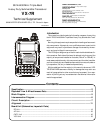
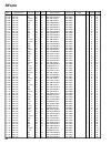
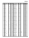
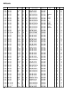
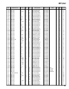
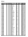
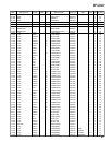
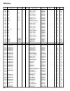
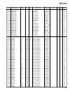
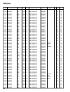
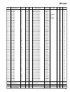
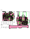
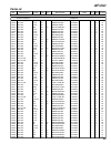
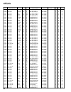
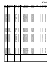
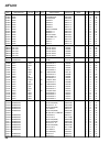
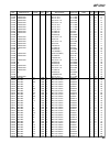
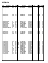
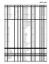
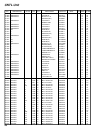
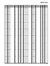
1 specification .................................................................................................................................... 2 exploded view & miscellaneous parts........................................................................................ 4 block diagram ............
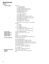
2 specifications general frequency ranges: channel steps: frequency stability: emission type: antenna impedance: supply voltage: current consumption: operating temperature: case size: weight: rx (main): 0.5 - 1.8 mhz (bc band) 1.8 - 30 mhz (sw band) 30-59 mhz (50 mhz ham: usa version) 30-76 mhz (50 ...
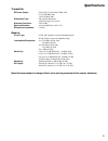
3 specifications are subject to change without notice, and are guaranteed within amateur bands only. Specifications transmitter rf power output: modulation type: maximum deviation: spurious emission: microphone impedance: receiver circuit type: intermediate frequencies: sensitivity: selectivity: af ...
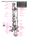
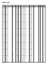
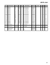
4 exploded view & miscellaneous parts À À Á Á Á Á Ã Ä ra0400000 rubber packing ra0417100 panel frame ra03995000 window ra03994000 double face tape ra0401600 o ring ra0399800 light guide (led) ra0400100 rubber knob (ptt) ra0140100 mask sheet ra0399700 holder (ptt) cp7342003 rear case ass’y with sma c...
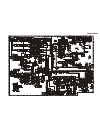
5 block diagram.
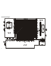
6 interconnection diagram.
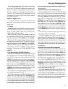
7 circuit description the vx-7r consists of a rf-unit, a cntl-unit and an af-unit. The rf-unit contains the receiver front end, pll ic, power and switching circuits, and the vco- unit for transmit and receive local signal oscillation. The cntl-unit contains the cpu, and audio ics, and the power circ...
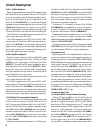
8 circuit description (5) 0.5 - 30 mhz reception received signals between 0.5 and 30 mhz pass through the triplexer circuit, low-pass filter circuit, hf t/r switch circuit and protector diode d1003 before additional fil- tering by a band-pass filter prior to application to rf amplifier q1009 (2sc491...
9 circuit description it switches q1048 (krc654u) to disable the receiver cir- cuits. This causes the "red" mode of busy/tx lamp d3033 to light. (2) modulation voice signal input from either built-in microphone mc3001 (em-140) on the cntl-unit or external jack j2002 on the af-unit is pre-emphasized ...
10 circuit description pll frequency synthesizer pll ic q1019 on the rf-unit consists of a data shift register, reference frequency divider, phase comparator, charge pump, "intermittent operation" circuit, and band selector switch. Serial pll data from the cpu is con- verted into parallel data by th...
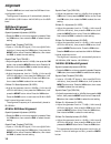
11 alignment introduction and precautions the vx-7r has been carefully aligned at the factory for the specified performance across the specified amateur bands. Realignment should therefore not be necessary except in the event of a component failure. All compo- nent replacement and service should be ...
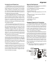
12 alignment test setup set up the test equipment as shown below for transceiv- er alignment, and apply 8.7 v dc power to the transceiv- er. Refer to the drawings for alignment points. Internal system alignment routine this uses a programmed routine in the transceiver which simplifies many previousl...
13 l1 tx power adjustment (l1 power) m transmit, and adjust the output power level for 50 mw (+50/-30 mw) by rotating the dial, then press the v/m button. Rotate the dial to select the next setting. Tx deviation adjustment (max dev) m inject a 1 khz audio tone at a level of 50 mv (rms) to the mic ja...
14 squelch preset threshold (thld sql) m inject a –15.0 dbµ rf signal (1 khz tone @ ±3.5 khz deviation), then press the v/m button, then press the mon/f button twice. Press the v/m button, then rotate the dial to select the next setting. Squelch preset tight (tigh sql) m adjust the generator level t...
15 high tx power adjustment (l3 power) m transmit, and adjust the output power level for 2.5 w (±0.2 w) by rotating the dial, then press the v/m but- ton. Rotate the dial to select the next setting. High tx power adjustment (l2 power) m transmit, and adjust the output power level for 1.0 w (±0.1 w) ...
16 alignment high tx power adjustment (hi power) m transmit, and adjust the output power level for 5.0 w (±0.3 w) by rotating the dial, then press the v/m but- ton. Rotate the dial to select the next setting. L3 tx power adjustment (l3 power) m transmit, and adjust the output power level for 2.5 w (...
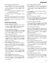
17 dcs tx deviation adjustment (dcs dev) m press the v/m button, then transmit and adjust the de- viation for 0.6 khz (±0.1 khz) by rotating the dial, then press the v/m button. Rotate the dial to select the next setting. Note: the next step depends on the geographical "version" of the transceiver b...
18 alignment press the sub button to activate the sub band inter- nal alignment routine. The alignment frequency will automatically be set to 435.100 mhz (usa version: 440.100 mhz) on the sub band. Sub band alignment 430 mhz band alignment squelch hysteresis adjustment (his sql) m rotate the dial fo...
19 rf unit circuit diagram ext dc in 13.8v ** :rx, ( ** ):tx 0.2v (0v) 430m rx:2.13v 0.66v (0v) 430m rx:2.7v 0v (5.5v) 50m rx:0v 0v (0v) 50m rx:0.45v 2.25v (1.6v) 50m: 1.99v (2.07v) 1.55v (1.6v) save:2.94v 0v (2.9v) 50m: 2.77v (0.48v) shift on:2.86v shift off:0v 0v (0v) 0v (2.9v) amrx:1.84v (amtx:2....
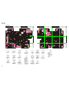
20 rf unit d side a parts layout side b 1ss321 (f9) (d1047) dan222 (n) (d1006, 1007, 1008, 1009, 1010, 1011, 1012, 1027, 1028, 1041, 1043, 1044, 1063) 1ss385 (09) (d1050) hn2d01fu (a1) (d1045, 1046) 2sa1774 (fr) (q1033, 1036, 1038, 1046, 1052) dtc143ze (e23) (q1025) dtc144ee (26) (q1001, 1026, 1029,...
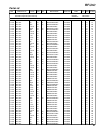
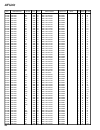
21 rf unit pcb with components (with vco unit) usa cb7372002 pcb with components (with vco unit) export cb7372003 pcb with components (with vco unit) germany cb7372004 printed circuit board fr008200c 1- c 1001 chip cap. 2pf 50v ck umk105ck020cw-f k22178250 1- a a1 c 1002 chip cap. 2pf 50v ck umk105c...
22 rf unit description value v/w tol. Vxstd p/n mfr’s desig vers. Ref. Lot. Side lay adr. C 1062 chip cap. 4pf 50v ch umk105ch040cw-f k22178252 1- a b2 c 1063 chip cap. 4pf 50v ch umk105ch040cw-f k22178252 1- a b2 c 1064 chip cap. 0.001uf 50v b umk105b102kw-f k22178829 1- a b2 c 1065 chip cap. 0.001...
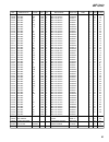
23 rf unit description value v/w tol. Vxstd p/n mfr’s desig vers. Ref. Lot. Side lay adr. C 1124 chip cap. 56pf 50v ch umk105ch560jw-f k22178276 1- b b2 c 1125 chip cap. 0.001uf 50v b umk105b102kw-f k22178829 1- a b2 c 1126 chip cap. 6pf 50v ch umk105ch060dw-f k22178254 1- a b2 c 1127 chip cap. 2pf ...
24 rf unit description value v/w tol. Vxstd p/n mfr’s desig vers. Ref. Lot. Side lay adr. C 1200 chip cap. 0.001uf 50v b umk105b102kw-f k22178829 1- b b3 c 1201 chip cap. 0.001uf 50v b umk105b102kw-f k22178829 1- b b3 c 1202 chip cap. 1uf 10v f grm39f105z10pt k22105001 1- b b3 c 1203 chip cap. 1uf 1...
25 rf unit description value v/w tol. Vxstd p/n mfr’s desig vers. Ref. Lot. Side lay adr. C 1258 chip cap. 0.001uf 50v b umk105b102kw-f k22178829 1- a a2 c 1259 chip cap. 2pf 50v ck umk105ck020cw-f k22178250 1- a a1 c 1260 chip cap. 0.001uf 50v b umk105b102kw-f k22178829 1- a a1 c 1262 chip cap. 1pf...
26 rf unit description value v/w tol. Vxstd p/n mfr’s desig vers. Ref. Lot. Side lay adr. C 1323 chip cap. 0.001uf 50v b umk105b102kw-f k22178829 1- d 1001 diode 1ss362 te85r g2070268 1- a b1 d 1002 diode 1ss362 te85r g2070268 1- b c2 d 1003 diode 1ss362 te85r g2070268 1- b c2 d 1004 diode 1sv271 tp...
27 rf unit description value v/w tol. Vxstd p/n mfr’s desig vers. Ref. Lot. Side lay adr. D 1061 diode rb751s-40te61 g2070850 1- b d1 d 1062 diode 1sv271 tph3 g2070476 1- a a1 d 1063 diode dan222 tl g2070174 1- b b2 d 1064 diode 1ss400 te61 g2070634 1- b a2 fb1001 chip coil blm21p300spt l1690840 1- ...
28 rf unit description value v/w tol. Vxstd p/n mfr’s desig vers. Ref. Lot. Side lay adr. L 1050 m.Rfc 0.1uh 2% c1608ca-r10g l1691045 1- a c1 l 1051 coil e2 0.25-1.85-8.5t-l l0022576 1- a c1 l 1052 coil e2 0.4-1.3-2t-l l0022580 1- a b2 l 1053 m.Rfc 4.7uh lk1608 4r7k-t l1690688 1- a b1 l 1054 coil e2...
29 rf unit description value v/w tol. Vxstd p/n mfr’s desig vers. Ref. Lot. Side lay adr. Q 1034 transistor dtc144ee tl g3070075 1- a b2 q 1035 transistor dtc144ee tl g3070075 1- a a1 q 1036 transistor 2sa1774 tl r g3117748r 1- a a3 q 1037 transistor kra760u-rtk g3070278 1- a b2 q 1038 transistor 2s...
30 rf unit description value v/w tol. Vxstd p/n mfr’s desig vers. Ref. Lot. Side lay adr. R 1043 chip res. 100k 1/16w 5% rmc1/16s 104jth j24189049 1- b c3 r 1044 chip res. 1k 1/16w 5% rmc1/16s 102jth j24189025 1- b d3 r 1045 chip res. 47k 1/16w 5% rmc1/16s 473jth j24189045 1- b d3 r 1046 chip res. 3...
31 rf unit r 1098 chip res. 100 1/16w 5% rmc1/16s 101jth j24189013 1- a c1 r 1099 chip res. 10k 1/16w 5% rmc1/16s 103jth j24189037 1- a c1 r 1100 chip res. 330 1/16w 5% rmc1/16s 331jth j24189019 1- a c1 r 1102 chip res. 3.3k 1/16w 5% rmc1/16s 332jth j24189031 1- b a3 r 1103 chip res. 2.2k 1/16w 5% r...
32 rf unit note:.
33 af unit circuit diagram busy:4.3v 0.4v (0.4v) 0v (0v) busy:0.55v 0.4v (0.4v) busy:1.33v 0v (0v) busy:9.2v 0v (0v) 12.8v (12.5v) busy:2.48v 0v (0v) 13.3v (13.1v) busy:3.0v 0v (0v) busy:3.0v 0v (0v) busy:0v 2.73v (2.76v) 2.7v (2.7v) 1.43v (1.43v) 1.6v (1.6v) 1.17v (1.17v) 0v (0v) 0v (0v) 0v (0v) 2....
34 af unit parts layout tda7233d (q2040) bu4094bcfv-e2 (q2048) dtc143ze (e23) (q2039) umb3n (b3) (q2003) dap222 (p) (d2001) 2sc5374 (na) (q2017, 2018, 2019, 2031) 2sj364-r(4m) (q2029, 2036, 2042, 2043, 2047) d side a a c 1 2 3 b side b d a c b 1 2 3 da221 (k) (d2003, 2017, 2018) mc2850 (a7) (d2012, ...
35 af unit *** af unit *** pcb with components cb1870001 printed circuit board fr008210c 1- c 2001 chip cap. 33pf 50v ch umk105ch330jw-f k22178270 1- b c2 c 2002 chip cap. 0.01uf 16v b grm36b103k16pt k22128804 1- b c2 c 2003 chip cap. 0.47uf 25v b grm40b474k25pt k22140824 1- a b2 c 2004 chip cap. 68...
36 af unit description value v/w tol. Vxstd p/n mfr’s desig vers. Ref. Lot. Side lay adr. C 2067 chip cap. 0.001uf 50v b umk105b102kw-f k22178829 1- a a1 c 2068 chip cap. 0.001uf 50v b umk105b102kw-f k22178829 1- a b1 c 2069 chip cap. 0.001uf 50v b umk105b102kw-f k22178829 1- a a1 c 2070 chip cap. 1...
37 af unit description value v/w tol. Vxstd p/n mfr’s desig vers. Ref. Lot. Side lay adr. C 2129 chip cap. 0.001uf 50v b umk105b102kw-f k22178829 1- a c2 c 2130 chip cap. 820pf 50v b grm36b821k50pt k22178808 1- a c2 c 2131 chip ta.Cap. 4.7uf 6.3v temsva20j475m-8r k78080031 1- a c2 c 2132 chip cap. 0...
38 af unit description value v/w tol. Vxstd p/n mfr’s desig vers. Ref. Lot. Side lay adr. D 2004 diode dan222 tl g2070174 1- b c1 d 2005 diode hvc355b(tape) g2070588 1- a a2 d 2006 diode 1sv325(tph3) g2070848 1- a a2 d 2007 diode dan222 tl g2070174 1- a d1 d 2008 diode dan222 tl g2070174 1- a b2 d 2...
39 af unit description value v/w tol. Vxstd p/n mfr’s desig vers. Ref. Lot. Side lay adr. Q 2019 transistor 2sc5374-tl g3353748 1- a b2 q 2020 transistor 2sa1774 tl r g3117748r 1- a c1 q 2021 transistor 2sa1774 tl r g3117748r 1- a c1 q 2022 transistor 2sc4154-t11-1e g3341548e 1- b b1 q 2023 transist...
40 af unit description value v/w tol. Vxstd p/n mfr’s desig vers. Ref. Lot. Side lay adr. R 2034 chip res. 4.7k 1/16w 5% rmc1/16s 472jth j24189033 1- a a1 r 2035 chip res. 22k 1/16w 5% rmc1/16s 223jth j24189041 1- a a1 r 2036 chip res. 10k 1/16w 5% rmc1/16s 103jth j24189037 1- a a1 r 2037 chip res. ...
41 af unit r 2097 chip res. 330k 1/16w 5% rmc1/16s 334jth j24189055 1- a c2 r 2098 chip res. 100k 1/16w 5% rmc1/16s 104jth j24189049 1- b c2 r 2099 chip res. 220 1/16w 5% rmc1/16s 221jth j24189017 1- b c2 r 2100 chip res. 330k 1/16w 5% rmc1/16s 334jth j24189055 1- b c2 r 2101 chip res. 22k 1/16w 5% ...
42 af unit note:.
43 cntl unit circuit diagram ext dc in 13.8v ** :rx, ( ** ):tx -5.88v -4.4v -2.92v 0v 1.5v 1.48v -4.4v -1.43v 1.51v -5.88v 0v 0v 0v 0v 0v 0v 0v 0v 0v 0v 3.0v 3.0v 0v (3.0v) pow off:0v chg:0v chg comp:3.0v 0v (0v) 0.25v (0v) 12.8v (12.6v) 2.4v (2.4v) 0v pow off:0v chg:0v comp:5.1v 0.74v pow off:0.74v...
44 cntl unit side a parts layout side b dan222 (n) (d3014) da221 (k) (d3015, 3016, 3017, 3018, ) hd6472237tf10 (q3035) njm3403av (q3018) rh5rh651a (q3028) dta144ee (16) (q3008) dtc143ze (e23) (q3037) dtc144ee (26) (q3007, 3011, 3013, 3014, 3015, 3019, 3036) umw1 (w1) (q3041) 2sc5374 (na) (q3038) 2sc...
45 cntl unit pcb with components cb1871002 usa pcb with components cb1871003 version a1 pcb with components cb1871004 version a2 pcb with components cb1871005 version a3 pcb with components cb1871006 version b1 pcb with components cb1871007 version b2 pcb with components cb1871008 version b3 pcb wit...
46 cntl unit description value v/w tol. Vxstd p/n mfr’s desig vers. Ref. Lot. Side lay adr. C 3046 chip cap. 1uf 10v f grm39f105z10pt k22105001 1- b d3 c 3047 chip ta.Cap. 220uf 4v sk4-0g227m-rd k78060014 1- b a2 c 3048 chip cap. 1uf 10v f grm39f105z10pt k22105001 1- b d4 c 3049 chip cap. 0.001uf 50...
47 cntl unit description value v/w tol. Vxstd p/n mfr’s desig vers. Ref. Lot. Side lay adr. C 3126 chip cap. 1uf 10v f grm39f105z10pt k22105001 1- b c2 c 3127 chip cap. 0.001uf 50v b umk105b102kw-f k22178829 1- b a2 c 3129 chip cap. 0.001uf 50v b umk105b102kw-f k22178829 1- b a4 c 3130 chip ta.Cap. ...
48 cntl unit description value v/w tol. Vxstd p/n mfr’s desig vers. Ref. Lot. Side lay adr. Q 3007 transistor dtc144ee tl g3070075 1- b a3 q 3008 transistor dta144ee tl g3070074 1- b a3 q 3009 transistor 2sc4154-t11-1e g3341548e 1- b a5 q 3010 ic njm12902v(te1) g1093592 1- b b6 q 3011 transistor dtc...
49 cntl unit description value v/w tol. Vxstd p/n mfr’s desig vers. Ref. Lot. Side lay adr. R 3026 chip res. 47k 1/16w 5% rmc1/16s 473jth j24189045 1- b a5 r 3027 chip res. 68k 1/16w 5% rmc1/16s 683jth j24189047 1- b a6 r 3028 chip res. 33k 1/16w 5% rmc1/16s 333jth j24189043 1- b a5 r 3029 chip res....
50 cntl unit description value v/w tol. Vxstd p/n mfr’s desig vers. Ref. Lot. Side lay adr. R 3087 chip res. 47k 1/16w 5% rmc1/16s 473jth j24189045 1- b b6 r 3088 chip res. 100k 1/16w 5% rmc1/16s 104jth j24189049 1- b a3 r 3088 chip res. 100k 1/16w 0.50% rr0510r-104-d j24189167 2- b a3 r 3089 chip r...
51 cntl unit description value v/w tol. Vxstd p/n mfr’s desig vers. Ref. Lot. Side lay adr. R 3150 chip res. 1m 1/16w 5% rmc1/16s 105jth j24189061 1- b c5 r 3151 chip res. 47k 1/16w 5% rmc1/16s 473jth j24189045 1- b b2 r 3152 chip res. 22k 1/16w 5% rmc1/16s 223jth j24189041 1- b c4 r 3153 chip res. ...
52 cntl unit note:.
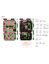
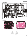
53 vco unit circuit diagram parts layout side a side b dtc143ze (e23) (q4001, 4003, 4007) ec3h07b (g) (q4002, 4004, 4005, 4006).
54 vco unit note.
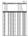
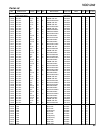
55 vco unit pcb with components cb1872001 printed circuit board fr007830d 1- c 4001 chip cap. 0.001uf 50v b umk105b102kw-f k22178829 1- a c 4002 chip cap. 0.01uf 16v b grm36b103k16pt k22128804 1- a c 4003 chip cap. 0.5pf 50v ck umk105ck0r5cw-f k22178247 1- a c 4004 chip cap. 0.01uf 16v b grm36b103k1...
56 vco unit d 4012 diode 1ss400 te61 g2070634 1- a d 4013 diode 1sv325(tph3) g2070848 1- a d 4014 diode hsc277trf g2070584 1- a d 4015 diode 1sv325(tph3) g2070848 1- a j 4001 connector axk5f10335p p1091136 1- b j 4002 connector axk5f10335p p1091136 1- b l 4001 m.Rfc 1uh lk1608 1r0k-t l1690687 1- a l...
57 vco unit note:.
58 vco unit copyright 2002 vertex standard co., ltd. All rights reserved no portion of this manual may be reproduced without the permission of vertex standard co., ltd. Printed in japan. E h 0 0 9 m 9 0 0

