Service manual important notice this manual has been provided for the use of authorized yamaha retailers and their service personnel. It has been assumed that basic service procedures inherent to the industry, and more specifically yamaha products, are already known and understood by the users, and ...
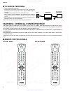
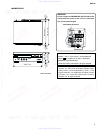
1 dsp-a5 ■ to service personnel 1. Critical components information components having special characteristics are marked ! And must be replaced with parts having specifications equal to those originally installed. 2. Leakage current measurement (for 120v model only) when service has been completed, i...
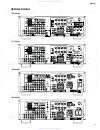
2 dsp-a5 ▼ t model ▼ b model ▼ g model ▼ r model ■ rear panels www. Xiaoyu163. Com qq 376315150 9 9 2 8 9 4 2 9 8 tel 13942296513 9 9 2 8 9 4 2 9 8 0 5 1 5 1 3 6 7 3 q q tel 13942296513 qq 376315150 892498299 tel 13942296513 qq 376315150 892498299 http://www.Xiaoyu163.Com http://www.Xiaoyu163.Com.
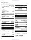
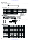
3 dsp-a5 ■ specifications ■ audio section minimum rms output power per channel (power amp. Section) main l/r, rear l/r 20hz to 20khz, 0.06% thd, 8 Ω 70w+70w 1khz, 0.09% thd, 8 Ω 80w+80w center 20hz to 20khz, 0.06% thd, 8 Ω 70w 1khz, 0.09% thd, 8 Ω 80w maximum power (eiaj) r, t models only main l/r, ...
4 dsp-a5 ● dimensions units: mm (inch) 21.5 (7/8") 435(17-1/8") 349.5(13-3/4") 390.5(15-3/8") 130(5-3/32") 151(5-15/16") 19.5 (13/16") 21 (27/32") warning do not change the impedance selector switch setting while the power to this unit is on, otherwise this unit may be damaged. Impedance selector ma...
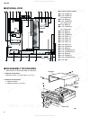
5 dsp-a5 ■ disassembly procedures (remove parts in disassembly order as numbered.) 1. Removal of top cover remove 4 screws ( 1 ) and 4 screws ( 2 ) in fig. 1. 2. Removal of front panel a. Remove 5 knobs. B. Remove 6 screws ( 3 ) in fig. 1. Fig.1 1 power transformer 2 p.C.B. Power (2) 3 p.C.B. Power ...
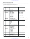
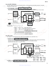
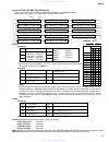
6 dsp-a5 ■ self diagnosis function 1. Purpose and operation the dsp-a5 has a self diagnosis function to locate a faulty part, if any, by inspecting and taking measurements. There are 12 main items in the diagnostic menu and have sub-menu items as listed below. No. 1 2 3 4 5 6 7 8 9 10 12 sub-menu 1....
7 dsp-a5 1. 2. 3. 4. 5. 6. 7. Effect level : muting : off input (video) : dvd/ld (dvd/ld) center speaker : large rear speaker : large main speaker : large lfe/bass out : swfr channel center r sur l sur swfr level (db) 0 0 0 0 c. Start-up display the protection history information appears on the fron...
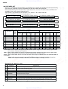
8 dsp-a5 ● protection history the following examples show how the protection history is displayed: appears when the protection function has not been activated. Displayed the check sum (4-digit, hexadecimal) and the version (one letter) of the main microcomputer. Appears when the current protection f...
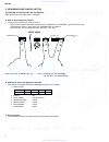
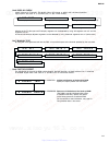
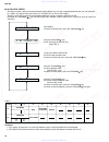
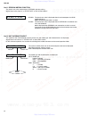
9 dsp-a5 ● selection by using the remote control unit the remote control codes in the menu list (see right column on page 8) correspond to the dsp program, test and effect keys. See the figure on the right. 3. Operation and display when starting diagnosis function (1) selection of diagnostic menu th...
10 dsp-a5 4. Contents of diagnosis function this section describes the contents of the self diagnosis function in detail. No.1 analog through the input is fixed to analog (a/d). There are two sub-menus. 1. Main bypass the l/r signals bypass the digital circuit, and are output to the main l/r. The l/...
11 dsp-a5 no.2 dsp through the input is automatically discriminated by signal detection and switched with priorities coaxial>optical>analog. There are the following three sub-menus. 1. Yss+sram the l/r signals are output without being processed to the main l/r through the ac3d2av. The l/r signals ar...
12 dsp-a5 no.3 ac-3/dts through the input is digital signal only. Ac-3 (dolby digital) or dts digital surround decoding operation is executed, according to the input source. 1. Status(binary form) ac-3 (dolby digital) decoded signals are output to each channel via ac3d2av. The ac-3 (dolby digital) s...
13 dsp-a5 1 main:sml 0db 7a-8b large large small 0db swfr l r none none none l+r 2 main:lrg 0db 7a-8c large large large 0db swfr l l none nonr none none 3 main:lrg -10 7a-8d large large large -10db swfr l l none none none none 4 b:main c:none 7a-8e none large large 0db main l l none none none none 5...
14 dsp-a5 no.6 display check check program for fl display. The display status will change as follows with sub-menu operation. Signal route is the same as "2. Effect off" of "no. 4 pro logic". A defect of the fl drive port and fl display segments can be detected by using "all segments turn off" and "...
15 dsp-a5 no.9 ad data check the a/d conversion values of the microcomputer which detects key scan port, protection detection port, etc. Are displayed in % (100%:5v). Signal route is the same as "2. Effect off" of "no. 4 pro logic". The keys on the main unit cannot be operated to detect the values o...
16 dsp-a5 no.10 status information from dsp the status data from the dsp block is sequentially displayed in a hexadecimal number. Signal route is the same as "2. Effect off" of "no. 4 pro logic". [cpu/1] [cpu/2] [note] when acmod is beyond 1000b, it is dts 7.1 signal. And the dsp block will be muted...
17 dsp-a5 1 2 r x - v a b g l the version and the check sum of the microcomputer software are displayed. A01: microcomputer software version. 824e: microcomputer software check sum. The model type and the destination are displayed. Rx-v: model type. Dsp-a= dsp-a5 rx-v = rx-v596, htr-5250 rds = rx-v5...
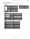
18 dsp-a5 ■ factory preset all of the system settings are initially set from the factory as follows. ● input selector ● effect level effect channel preset value center 0 db right surround 0 db left surround 0 db subwoofer 0 db ● dsp program no. Program sub-program delay preset value dolby/dts normal...
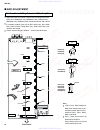
19 dsp-a5 confirmation of idling current of main amplifier • right after power is turned on, confirm that the voltage across the terminals of r688(main lch),r690(main rch), r692(center), r694(rear lch), r696(rear rch) are between 0.1mv and 10.0mv. • if it exceeds 10.0mv, open (cut off) r571 (main lc...
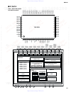
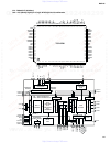
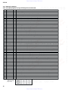
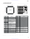
20 dsp-a5 ■ ic data ic501 : m30217ma-a203fp 16-bit microcomputer p50/fl08 p51/fl09 p52/fl10 p53/fl11 p54/fl12 p55/fl13 p56/fl14 p57/fl15 p00/fl16 p01/fl17 p02/fl18 p03/fl19 p04/fl20 p05/fl21 p06/fl22 vss p07/fl23 vcc p10/fl24 p11/fl25 p24/fl36 p25/fl37 p26/fl38 p27/fl39 p30/fl40 p31/fl41 p32/fl42 p3...
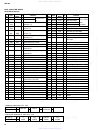
21 dsp-a5 ic501 : m30217ma-a203fp 16-bit microcomputer *1 model type distinction (h=1, l=0) dsp-a (pin 3) 0 0 1 rx-v596 1 rx-v596rds rds (pin 6) 0 1 0 htr-5250 1 *2 destination distinction of tuner (h=1, l=0) v1 (pin 4) 0 j 0 u,c 1 a,b,g,l 1 r,t v2 (pin 5) 0 model 1 models 0 models 1 models dsp-a5 d...
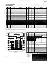
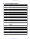
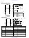
22 dsp-a5 ic107 : bu2090 serial input/parallel output driver for output port expansion pin pin port i/o function no. Name 67 p05/fl21 p1 o segment 1 for fl display 68 p04/fl20 p2 o segment 2 for fl display 69 p03/fl19 p3 o segment 3 for fl display 70 p02/fl18 p4 o segment 4 for fl display 71 p01/fl1...
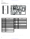
23 dsp-a5 ic3 : ysd917 (dir5) digital format interface receiver 1 2 3 4 5 6 7 8 9 10 11 12 13 14 28 27 26 25 24 23 22 21 20 19 18 17 16 15 avdd pco avss m/s ddin test /ic vss xo xi mck vdd sdo sdbck sck si so /cs vdd int /lock err dbl fs128 sync vss sdmck sdwck digit al a udio interf a ce decoder & ...
24 dsp-a5 vss ramd7 ramd6 ramd5 ramd4 ramd3 ramd2 ramd1 ramd0 vdd1 rama2 sck si so /cs /csb rama3 test /ic rama4 pvss sdwck1 sdbck1 sdob0 sdob1 sdob2 rama7 rama8 rama9 vdd2 vss oport7 oport6 oport5 oport4 oport3 oport2 oport1 oport0 vdd1 vdd sdwck0 sdbck0 sdia0 sdia1 rama1 rama0 ramwen ramoen vss vd...
25 dsp-a5 no. Name i/o function 1 vdd1 +5v power supply 2 ramcen o ram chip enable output terminal (normally unconnected) 3 rama16 o ram address output terminal 16, connected to external 1m sram address 4 rama15 o ram address output terminal 15, connected to external 1m sram address 5 sdib0 i serial...
26 dsp-a5 ic4 : yss918d-f (ac3d2av) dsp + ac-3(dolby digital)/ pro logic/ dts digital surround decoder 51 vdd2 +3v power supply 52 nonpcm o non-pcm data output terminal, non-pcm data detect output 53 crc o crc output terminal (normally unconnected) 54 mute o mute output terminal, connected to extern...
27 dsp-a5 ic5 : is61c1024-20j (1m sram) 131072-word x 8-bit high speed static ram nc a3 a4 a5 a6 a7 a8 a9 a10 a11 a12 a13 d1 d2 d3 gnd 1 2 3 4 5 6 7 8 9 10 11 12 13 14 15 16 vcc a2 ce2 /we a1 a0 a16 a15 /oe a14 /ce1 d8 d7 d6 d5 d4 32 31 30 29 28 27 26 25 24 23 22 21 20 19 18 17 decoder top view a0-a...
28 dsp-a5 ic6 : ak4526a-vq (codec. Adc/dac) 20-bit 6-channel a/d, d/a converter vr vr vr vr vr vr lpf dac lpf dac lpf dac lpf dac lpf dac lpf dac sdos ocks m/s bick lrck sdti1 sdti2 sdti3 sdto daux dfs dem1 dem0 mcko dvdd dvss /pd xts icks1 icks0 cad1 cad0 cdto cdti cclk /cs p/s mcki xti avss avdd v...
29 dsp-a5 ■ display data ● v501 : 16-bt-71gk (v4193300) • grid assignment • pin connection • anode connection y 1 pattern area 18 fd 17 16 15 14 13 12 np 11 np 10 np np np np np np 9 np 8 np 7 np 6 np 5 np 4 np 3 np 2 f1 1 f1 pin no. Connection 19 fd 20 np 21 np 22 p22 23 p21 24 p20 25 p19 43 p1 42 ...
Dsp-a5 e-30/j-28 e-31/j-29 ■ block diagram 10 11 21 20 6-ch selector ic102 26 25 27 6 5 4 8 9 7 22 23 24 operation key sw503-510 43 93 28 19 64 21 12 20 16 63 99 46 reset q503,d502 power down detect q504,d510,511 back-up (memory) ic502 d512 regulator q802, d803 1 2 64 65 43 22 ~ 61 46 ~ u501 /st sck...
Dsp-a5 e-30/j-28 e-31/j-29 ■ block diagram 10 11 21 20 6-ch selector ic102 26 25 27 6 5 4 8 9 7 22 23 24 operation key sw503-510 43 93 28 19 64 21 12 20 16 63 99 46 reset q503,d502 power down detect q504,d510,511 back-up (memory) ic502 d512 regulator q802, d803 1 2 64 65 43 22 ~ 61 46 ~ u501 /st sck...
A 1 2 3 4 5 6 8 dsp-a5 b c d e f g h i j k l 7 e-51/j-49 ■ schematic diagram [dsp] ★ all voltages are measured with a 10m Ω /v dc electric volt meter. ★ components having special characteristics are marked and must be replaced with parts having specifications equal to those originally installed. ★ s...
A 1 2 3 4 5 6 7 8 dsp-a5 b c d e f g h i j k front l front l rear l reae l reae l main l main l (dsp) main l (dsp) main l main l main l (dsp) main l center center center main l center lfe lfe lfe 12 .0 12 .0 0 0 0 0 -11.6 4.8 12 .0 12 .0 0 0 0 0 -11.6 4.8 12 .0 0 0 0 0 0 0 0 11.4 –11.0 0 0 -11.6 4.8...
A 1 2 3 4 5 6 8 dsp-a5 b c d e f g h i j k l 7 e-49/j-47 ■ schematic diagram [input (2/2)] digital in 4.7 0 0 0 0 0 0 0.1 4.7 4.7 0.1 0 0 4.7 4.7 4.7 4.7 4.7 4.7 4.7 0 0 0 0 0.3 0.3 4.7 4.7 4.7 0 0 0 0 4.7 4.7 4.7 4.7 0 0 0 0 0 0 0 0 0 0 0 0 0 0 0 3.0 0.3 4.1 0.1 4.7 4.7 4.7 4.7 4.7 0 0 4.7 0 0 0 0 ...
A 1 2 3 4 5 6 7 8 dsp-a5 b c d e f g h i j k e-52/j-50 ■ schematic diagram [main (1/2)] rear l rear l main l center main l center main l 44.5 43.9 44.4 20.6 1.0 44.4 –0.7 30.7 30.7 30.7 0 20.4 0 0 0 0 0 –0.7 43.3 44.4 –0.7 –0.1 –0.1 44.0 43.3 1.0 44.4 0 –0.6 43.3 0 –0.6 –0.1 –0.7 43.3 43.3 43.3 1.0 ...
A 1 2 3 4 5 6 8 dsp-a5 b c d e f g h i j k l 7 e-53/j-51 ■ schematic diagram [main (2/2), power] rear l main l center lfe 0 0 0 0 –33.6 45.0 0 0 –45.1 ac71.1v(54.2v) 32.9 12.8 6.5 12.8 0 0.7 0 0 6.5 0 0 6.3 6.3 12.8 ac12.8v ac48.1v ac32.2v ac9.8v 5.2 19.9 –19.9 0 0 0 30.2 –30.2 0 0 5.1 10.5 5.0 0 9....
A 1 2 3 4 5 6 7 8 dsp-a5 b c d e f g h i j k main l 3 4 –27 .7 –27 .7 –27 .7 –27 .7 –27 .7 –27 .7 –25 .3 –27 .7 –27 .7 –23 .2 –23 .3 –21 .4 –25 .5 –25 .2 –27 .7 –23 .6 –13 .6 –11 .0 –13 .5 –21 .3 –19 .5 –13 .4 –25.7 –25.7 –25.7 –25.7 –25.7 –25.7 –25.7 –25.7 –25.7 –25.7 –25.7 –25.7 –25.7 –25.7 –27.7 ...
Dsp-a5 e-40/j-38 e-41/j-39 b a c d e f h g 1 2 3 4 5 6 ■ printed circuit board (foil side) p. C. B. Dsp p. C. B. Dsp ref. No. Location d1 f3 d2 f3 d4 d4 d5 g4 d6 g4 d7 g4 d8 g4 d9 g4 d10 g4 d11 g4 d12 g4 d14 d4 d15 d4 d16 d4 d17 d4 d150 h4 d151 g4 d152 h4 ● semiconductor location ref. No. Location i...
Dsp-a5 p. C. B. Operation (2) p. C. B. Operation (3) p. C. B. Operation (1) h e-42/j-40 b a c d e f g 1 2 3 4 5 6 ■ printed circuit board (foil side) e-43/j-41 pr v2 celc dtb vdn /csd cea c1 sck sckd mg sod clka c rxa c cea c2 erra /st do rce rck f-rx fce mg cnvss f-tx f-ck +5bu /res cetc ckb vup ce...
Dsp-a5 p. C. B. Input (4) p. C. B. Input (3) p. C. B. Input (2) e-44/j-42 b a c d e f h g 1 2 3 4 5 6 ■ printed circuit board (foil side) e-45/j-43 p. C. B. Input (5) to: input (1) e ve aux-c axr axl aux-y aux-v axr e axl e sw5 sw4 sw3 sw2 sw1 –5 +5 #303 #303 monit or out vcr in out d vd/ld d-tv cbl...
Dsp-a5 –12 81 tc9299p 91 6 81 tc9299p 9 1 9 1 8 njm2068ld 81 njm2068ld 1 28 15 14 tc9273n-004 1 18 m5220l 1 8 m5220l 30 16 15 lc78213 1 30 16 15 lc78212 m8220l 16 /csd sid sod dg +12 cecod cea c1 sckd +5d intd clka c rxa c cea c2 /ica c txa c dbl /icd erra to:dsp #3 #3 #3 e fr lfe rr rin e fl c rl l...
Dsp-a5 p. C. B. Main (6) p. C. B. Main (3) e-36/j-34 e-37/j-35 b a c d e f g 1 2 3 4 5 6 ■ printed circuit board (foil side) p. C. B. Main (4) h e +b +bv vc nfc vrr nfrr vrl nerl vr nfr vl nfl –bv t o:main (1) ce re pr v1 -bl bl mg s12 pr y +25 –25 +10 +5d +5 –5 +12 –12 vg fr om: po wer(3) pry pry s...
Dsp-a5 p. C. B. Main (5) h e-38/j-36 b a c d e f g 1 2 3 4 5 6 ■ printed circuit board (foil side) e-39/j-37 p. C. B. Main (2) output rear (surr ound) center rear (surr ound) center r speakers l r l + – speakers +– – + main r l b a fr om:main (6) e +b +bv vc nfc vrr nfrr vrl nfrl vr nfr vl nfl –bv w...
Dsp-a5 pr y pr y si2 si2 mg mg w856 br w854 be w855 or w856b w802b w854b w852b w855b w851b w853b w801b w852 wh w853 re w851 ye w801 gy w802 br w853a w852a w851a w855a w856a w802a w801a w854a t o:po wer transformer to:main(3) 1 2 3 4 5 6 7 8 voltage selector switched 100w max. T o t al a c outlets • ...
Dsp-a5 p. C. B. Power (5) p. C. B. Power (3) p. C. B. Power (1) h e-34/j-32 b a c d e f g 1 2 3 4 5 6 ■ printed circuit board (foil side) e-35/j-33 vg dg +b3 –b3 e +b2 –b4 +b4 vg –12 +12 –5 +5 +5d +10 –25 +25 t o:main (6) +b4 –b4 +b2 e –b2 +b3 dg vg w451 w452 ac1 ac2 e ac2 ac1 ac3 ac3 fr om:po wer t...
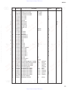
54 dsp-a5 parts list ■ electrical parts abbreviations in this list are as follows: c. A. El. Chp : chip alumi. Electrolytic cap c. Ce : ceramic cap c. Ce. Array : ceramic cap array c. Ce. Chp : chip ceramic cap c. Ce. Ml : multilayer ceramic cap c. Ce. M. Chp : chip multilayer ceramic cap c. Ce. Saf...
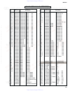
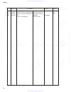
55 dsp-a5 p. C. B. Dsp schm ref part no. Description ✻ new parts ✻ new parts schm ref part no. Description ✻ ✻ v4800100 p.C.B. Dsp cb1 vq044300 cn.Bs.Pin 7p cb3 vq044900 cn.Bs.Pin 19p cb6 vq044600 cn.Bs.Pin 13p c1 ub245100 c.Ce.M.Chp 0.1uf 25v c2 ub052100 c.Ce.M.Chp 100pf 50v c3 ub052100 c.Ce.M.Chp ...
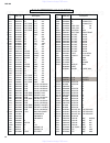
56 dsp-a5 schm ref part no. Description ✻ new parts ✻ new parts schm ref part no. Description p. C. B. Dsp & p. C. B. Operation c138 ub245100 c.Ce.M.Chp 0.1uf 25v c139 ub052100 c.Ce.M.Chp 100pf 50v c140 ub052100 c.Ce.M.Chp 100pf 50v c141 ub052100 c.Ce.M.Chp 100pf 50v c150 ub052100 c.Ce.M.Chp 100pf 5...
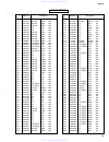
57 dsp-a5 p. C. B. Operation & p. C. B. Input schm ref part no. Description ✻ new parts ✻ new parts schm ref part no. Description c511 vj599100 c.Ce.Tublr 0.1uf 50v c512 ur847470 c.El 47uf 25v c513 vj599100 c.Ce.Tublr 0.1uf 50v c514 vj599100 c.Ce.Tublr 0.1uf 50v c515 vj599100 c.Ce.Tublr 0.1uf 50v c5...
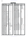
58 dsp-a5 p. C. B. Input schm ref part no. Description ✻ new parts ✻ new parts schm ref part no. Description c110 ua952100 c.Mylar 100pf 50v c111 ua952100 c.Mylar 100pf 50v c112 ua952100 c.Mylar 100pf 50v c113 ua952100 c.Mylar 100pf 50v c114 fg651470 c.Ce 47pf 50v c115 fg651470 c.Ce 47pf 50v c116 ua...
59 dsp-a5 p. C. B. Input schm ref part no. Description ✻ new parts ✻ new parts schm ref part no. Description c356 ur837100 c.El 10uf 16v c357 vf466800 c.Ce.Tublr 100pf 50v c358 vf466800 c.Ce.Tublr 100pf 50v c360 ur837330 c.El 33uf 16v c362 ur837330 c.El 33uf 16v c363 ur837470 c.El 47uf 16v c364 ur83...
60 dsp-a5 p. C. B. Power schm ref part no. Description ✻ new parts ✻ new parts schm ref part no. Description v4801900 p.C.B. Power(b) v4802000 p.C.B. Power(g) v4802400 p.C.B. Power(rt) cb401 vq045300 cn.Bs.Pin 23p cb451 vi878600 cn.Bs.Pin 8p cb721 vq963000 cn.Bs.Pin 9p cb722 vi878600 cn.Bs.Pin 8p cb...
61 dsp-a5 p. C. B. Power & p. C. B. Main schm ref part no. Description ✻ new parts ✻ new parts schm ref part no. Description r451 hv753100 r.Car.Fp 1 Ω 1/4w r452 hv753100 r.Car.Fp 1 Ω 1/4w r725 hv753100 r.Car.Fp 1 Ω 1/4w r726 hv753100 r.Car.Fp 1 Ω 1/4w r727 hv755100 r.Car.Fp 100 Ω 1/4w r728 hv755100...
62 dsp-a5 schm ref part no. Description ✻ new parts ✻ new parts schm ref part no. Description p. C. B. Main c760 vg291300 c.El 100uf 50v c761 vg291300 c.El 100uf 50v c762 ua655100 c.Mylar 0.1uf 50v c763 ua655100 c.Mylar 0.1uf 50v d501 vg439600 diode.Zenr mtzj10c 10v d502 vd631600 diode 1ss133,176,hs...
63 dsp-a5 schm ref part no. Description ✻ new parts ✻ new parts schm ref part no. Description p. C. B. Main r566 hv755100 r.Car.Fp 100 Ω 1/4w r567 vt975300 r.Mtl.Oxd 3.9k Ω 1w r569 v3946100 r.Mtl.Oxd 2.7k Ω 0.5w r570 v3945100 r.Mtl.Oxd 390 Ω 0.5w r571 v3945600 r.Mtl.Oxd 1k Ω 0.5w r572 v3945500 r.Mtl...
Dsp-a5 64 65 ✻ new parts rd254470 r.Car.Chp 47 Ω 1/10w rd255100 r.Car.Chp 100 Ω 1/10w rd255330 r.Car.Chp 330 Ω 1/10w rd256100 r.Car.Chp 1k Ω 1/10w rd256120 r.Car.Chp 1.2k Ω 1/10w rd256150 r.Car.Chp 1.5k Ω 1/10w rd256220 r.Car.Chp 2.2k Ω 1/10w rd256330 r.Car.Chp 3.3k Ω 1/10w rd256360 r.Car.Chp 3.6k Ω...
Dsp-a5 66 b a c d 1 2 3 4 5 6 ■ mechanical parts ref. No. Part no. Description remarks markets ✻ new parts 67 ■ exploded view jk ass'y vr ass'y sw ass'y vr ass'y b model g model 1-4 1-5 162 1-1 124 162 123 122 121 2-113 2-114 101 171 162 171 25 2-8 28 17 16 160 163 166 161 160 160 160 176 2-108 103 ...
68 dsp-a5 ref. No. Part no. Description remarks markets ✻ new parts 25 mf123140 flexible flat cable 23p 140mm 26 mf113140 flexible flat cable 13p 140mm 27 mf207200 s flexible flat cable 7p 200mm 28 mf207350 s flexible flat cable 7p 350mm 101 vv121300 top cover bl 101 vv121500 top cover ti 101 vz8845...
69 dsp-a5 ref. No. Part no. Description remarks markets ✻ new parts accessories 200 v4297600 remote control transmitter sbgh20018a rav210 (rt) 200 v4297700 remote control transmitter sbgh20018a rav211 (bg) 200-1 aax14030 lid bw0780/1 71078002000 battery, manganese sum-4,aaa,r03 ✻ ✻ ✻ www. Xiaoyu163....
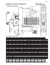
■ remote control transmitter schematic diagram 37 29 30 31 32 35 34 20 12 nc 25 p30/intp0 p07 nc p06 p05 p04 p01 p02 p52 11 3 2 1 44 43 42 41 40 dvd/ld dvd menu tv cable/sat cd vcr tape/md amp/tuner sw1 jrs1901 dsp/tuner 10 9 8 7 6 scl sda u2 r2 1k Ω r1 1k Ω 6 5 vdd vdd vdd vdd wp 8 vss 4 c3 0.1 µ f...
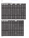
Key key dvd dvd menu ld cd no. Name yamaha 0008 yamaha 0008 yamaha 0007 yamaha 0005 yamaha 0015 3 1 1 7c-94 1 7c-94 1 7c-17 1 79-11 79-11 4 2 2 7c-95 2 7c-95 2 7c-18 2 79-12 79-12 5 3 3 7c-96 3 7c-96 3 7c-19 3 79-13 79-13 6 4 4 7c-97 4 7c-97 4 7c-1a 4 79-14 79-14 7 5 5 7c-98 5 7c-98 5 7c-1b 5 79-15 ...

