- DL manuals
- Yamaha
- Amplifier
- DSP-AX620
- Service Manual
Yamaha DSP-AX620 Service Manual
AV AMPLIFIER
1 0 0 7 6 3
This manual has been provided for the use of authorized YAMAHA Retailers and their service personnel.
It has been assumed that basic service procedures inherent to the industry, and more specifically YAMAHA Products, are already
known and understood by the users, and have therefore not been restated.
WARNING:
Failure to follow appropriate service and safety procedures when servicing this product may result in personal
injury, destruction of expensive components, and failure of the product to perform as specified. For these
reasons, we advise all YAMAHA product owners that any service required should be performed by an
authorized YAMAHA Retailer or the appointed service representative.
IMPORTANT:
The presentation or sale of this manual to any individual or firm does not constitute authorization, certification
or recognition of any applicable technical capabilities, or establish a principle-agent relationship of any
form.
The data provided is believed to be accurate and applicable to the unit(s) indicated on the cover. The research, engineering, and
service departments of YAMAHA are continually striving to improve YAMAHA products. Modifications are, therefore,
inevitable and specifications are subject to change without notice or obligation to retrofit. Should any discrepancy appear to exist,
please contact the distributor's Service Division.
WARNING:
Static discharges can destroy expensive components. Discharge any static electricity your body may have
accumulated by grounding yourself to the ground buss in the unit (heavy gauge black wires connect to this
buss).
IMPORTANT:
Turn the unit OFF during disassembly and part replacement. Recheck all work before you apply power to the
unit.
IMPORTANT NOTICE
DSP-AX620
SERVICE MANUAL
■
CONTENTS
TO SERVICE PERSONNEL ........................................... 1
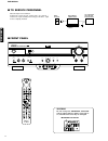
FRONT PANEL ............................................................... 1
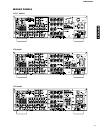
REAR PANELS ............................................................... 2
SPECIFICATIONS ..................................................... 3 – 5
INTERNAL VIEW ............................................................ 5
DISASSEMBLY PROCEDURES .............................. 6 – 8
SELF DIAGNOSIS FUNCTION ............................... 9 – 27
AMP CHECK ................................................................. 28
IC DATA ................................................................ 29 – 36
DISPLAY DATA .................................................... 37 – 38
PIN CONNECTION DIAGRAM ..................................... 39
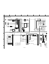
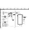
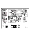
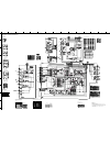
BLOCK DIAGRAM ................................................ 40 – 43
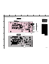
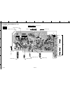
PRINTED CIRCUIT BOARD ................................. 44 – 67
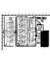
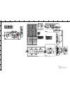
SCHEMATIC DIAGRAM ....................................... 68 – 73
PARTS LIST .......................................................... 74 – 92
REMOTE CONTROL TRANSMITTER .................. 93 – 95
DSP-AX620
Summary of DSP-AX620
Page 1
Av amplifier 1 0 0 7 6 3 this manual has been provided for the use of authorized yamaha retailers and their service personnel. It has been assumed that basic service procedures inherent to the industry, and more specifically yamaha products, are already known and understood by the users, and have th...
Page 2
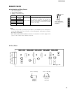
Dsp-ax620 dsp-ax620 ■ to service personnel critical components information components having special characteristics are marked z and must be replaced with parts having specifications equal to those originally installed. Ac leakage tester or equivalent equipment under test insulating table wall outl...
Page 3
Dsp-ax620 dsp-ax620 2 ▼ r, t models ■ rear panels 240v 50 ▼ b model ▼ g model.
Page 4
Dsp-ax620 dsp-ax620 3 ■ general power supply b, g models . . . . . . . . . . . . . . . . . . . . . . . Ac 230v, 50hz r, t models . . . . . . . . . . . Ac 110/120/220/240v, 50/60hz power consumption . . . . . . . . . . . . . . . . . . . . . . . . . . . 260w standby power consumption b, g models . . ....
Page 5
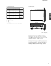
Dsp-ax620 dsp-ax620 4 ● dimensions 352.5 (13–7/8") 390 (15–5/16") 16 (5/8") 435 (17–1/8") 21 (13/16") 21.5 (13/16") 130 (5–1/8") 151 (5–15/16") units : mm (inch) manufactured under license from dolby laboratories. "dolby digital", "ac-3", "pro logic", and the double-d symbol v are trademarks of dolb...
Page 6
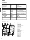
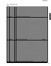
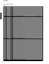
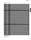
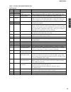
Dsp-ax620 dsp-ax620 5 ■ internal view ● set menu table no. Set menu preset value setting ranges 1. Speaker set 1a center speaker large large/small/none 1b main speaker large large/small 1c rear l/r speaker large large/small/none 1d lfe/bass out both subwoofer/main/both 1e main level normal normal/–1...
Page 7
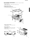
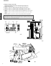
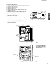
Dsp-ax620 dsp-ax620 6 ■ disassembly procedures (remove parts in the order as numbered.) 1. Removal of top cover remove 8 screws ( q and w ) and then remove the top cover in fig. 1. 2. Removal of front panel unit a. Remove 9 screws ( e , r and t ) in fig. 1. B. Remove cb104, cb303 and ground wire. C....
Page 8
Dsp-ax620 dsp-ax620 7 5. Removal of input (1)/(2) p.C.B. (checking the input (1)/(2) p.C.B. And replacing components) a. Remove the dsp p.C.B. B. Remove 1 screw ( !0 ) and then remove the input (4) p.C.B. In fig. 4. C. Remove 2 screws ( !1 ) and then remove the operation (5) p.C.B. In fig. 4. D. Rem...
Page 9
Dsp-ax620 dsp-ax620 8 6. Removal of main chassis (checking the main (1) p.C.B. And replacing components) a. Remove the front panel unit. B. Remove the sub chassis unit. C. Remove the dsp p.C.B. Fig. 7 fig.8 fig.9 d. Remove the input (4) p.C.B, operation (5)/(3)/(2) p.C.B. And input (1)/(2) p.C.B. E....
Page 10
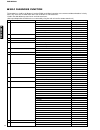
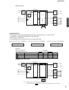
Dsp-ax620 dsp-ax620 9 ■ self diagnosis function this product has a built-in self diagnosis function (diag) to facilitate inspection, measurement and determination of a faulty item, if any. There are 14 diag menu items each of which has sub-menu items. Listed in the table below are menu items and sub...
Page 11
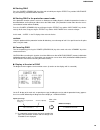
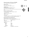
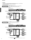
Dsp-ax620 dsp-ax620 10 ● starting diag press the “power” (standby/on) key of the main unit while pressing the “effect” key and the “input mode” key simultaneously, and diag will be activated. ● starting diag in the protection cancel mode if the protection function activates and causes hindrance to t...
Page 12
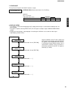
Dsp-ax620 dsp-ax620 11 if the protection function activates after diag has been started and the power is turned off ; when the protection function (*2) activates, the protection function history appears on the display and the power turns off. Repair the faulty parts according to the displayed histor...
Page 13
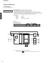
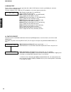
Dsp-ax620 dsp-ax620 12 ● operation procedure of diag menu and sub-menu there are 14 menu items and some sub-menu items as well. Diag menu selection main unit: jog dial w (forward)/ q (reverse) remote control unit: cursor n (forward)/ b (reverse) key sub-menu selection main unit: dsp program (forward...
Page 14
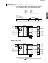
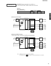
Dsp-ax620 dsp-ax620 13 1. Dsp through there are 6 sub menu items. Details of diag menu note: (sdoxx) represents a terminal name of ac3d3. The shaded square ( ) means that the element included in it does not operate. Analog bypas [remote control code: 7a—88(prg 1)] • the input mode is fixed to use th...
Page 15
Dsp-ax620 dsp-ax620 14 swfr rl rr fl fr c l r d/a ak4382 codec (d/a) ak4527 l/r l/r l/r l/r sdob0 sdob2 sdob1 sdob3 codec (a/d) ak4527 dir pcm thr main dsp (decoder) sub dsp digital analog ac3d3 yss928 4m dram 0db 0db/-20db mute -12db (in the case of 2-ch source) swfr rl rr fl fr c l r d/a ak4382 co...
Page 16
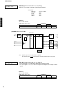
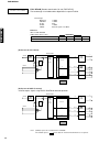
Dsp-ax620 dsp-ax620 15 full bit [remote control code: 7a—91 (prg 10)] • the head margin is unused and the digital data is output in full bit. • the same applies as “m, c, r, sw ch” except that the digital data is output in full bit at d/a . Swfr rl rr fl fr c l r d/a ak4382 codec (d/a) ak4527 l/r l/...
Page 17
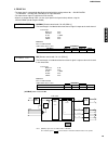
Dsp-ax620 dsp-ax620 16 full bit f [remote control code: 7a—92 (prg 11)] the front channel signal is output in full bit to the main channel. (in the case of multi-ch source) • ac3d3 outputs signals using dolby digital/dts decode operation. Note: (sdoxx) represents a terminal name of ac3d3. The shaded...
Page 18
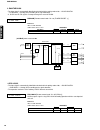
Dsp-ax620 dsp-ax620 17 full bit-6db [remote control code: 7a—03 (tape stop)] the head margin is included and the digital data is output in half bit. (in the case of multi-ch source) • ac3d3 outputs signals using dolby digital/dts decode operation. Note: (sdoxx) represents a terminal name of ac3d3. T...
Page 19
Dsp-ax620 dsp-ax620 18 note: (sdoxx) represents a terminal name of ac3d3. The shaded square ( ) means that the element included in it does not operate. 2. Front ch • the input signal is automatically identified and switched in the priority order of dts ➝ dolby digital ➝ pcm audio ➝ analog (a/d) acco...
Page 20
Dsp-ax620 dsp-ax620 19 4. Pro logic • the input signal is automatically identified and switched in the priority order of dts ➝ dolby digital ➝ pcm audio ➝ analog (a/d) according to the signal detection. • the operation conforms to the ordinary dolby normal sound field. Pro logic [remote control code...
Page 21
Dsp-ax620 dsp-ax620 20 swfr rl rr fl fr c l r d/a ak4382 codec (d/a) ak4527 l/r l/r c/mute s sdob0 sdob2 sdob1 sdob3 codec (a/d) ak4527 dir dd/dts decoder main dsp (decoder) sub dsp digital analog ac3d3 yss928 4m dram -3db -3db/mute mute -12db c/s (2ch) *multi: all mute 5. Margin check • the input s...
Page 22
Dsp-ax620 dsp-ax620 21 6. Main mix • the input signal is automatically identified and switched in the priority order of dts ➝ dolby digital ➝ pcm audio ➝ analog (a/d) according to the signal detection. • there are two sub-menu items. • the center and sw signals are output through the main channel. 6...
Page 23
Dsp-ax620 dsp-ax620 22 8. Display check • this program is used to check the lighting of the fl display which changes as shown below according to the sub- menu selected. • the signals are processed using effect off. (the l/r signals are output using the analog main bypass setting.) • except for the i...
Page 24
Dsp-ax620 dsp-ax620 23 10. Factory preset this menu reserves and inhibits initialization of the back-up ram (parameter, set menu contents, etc. For the sound field program). The signals are processed using effect off. (the l/r signals are output using analog main bypass set- ting.) rsrv (initializat...
Page 25
Dsp-ax620 dsp-ax620 24 11. Ad data the sub-menu of this menu displays the a/d conversion value of the cpu (operation circuit board ic501) which detects the keys and protection functions of the main unit in %. (reference voltage 5v: 100%) when in ky0/ky1/ky2 page, it is not possible to operate the ke...
Page 26
Dsp-ax620 dsp-ax620 25 12. If status (input function status) using this menu, the status data is displayed in the hexadecimal notation one after another. During signal processing, the status before execution of this menu is maintained. To convert the analog input to the digital input, use the follow...
Page 27
Dsp-ax620 dsp-ax620 26 bit7 mute requested bit6 dts flashing (red) bit5 ex sound field being processed bit4 full mute (on: 1) bit3 – bit2 through & bypass (*2) bit1 – bit0 dts analog mute 5th byte indicates the information on the signal processing status. (*2): in the case of digital signals other t...
Page 28
Dsp-ax620 dsp-ax620 27 14. Version/sum there are two sub-menu items. Indicates the program version, checksum of the microprocessor (ic501 of the operation circuit board). The checksum is obtained by adding data for every 8 bits for each program area and expressing the result as a 4-figure hexadecima...
Page 29
Dsp-ax620 dsp-ax620 28 ■ amp check ● confirmation of idling current 1) no signal applied. 2) non-loaded condition. 3) aging is not neccessary. Test point r145 r150 r165 r155 r160 rating (dc) 0.1mv—10mv note item main l main r center rear l rear r if the measured voltage exceeds 10.1mv, cut the lead ...
Page 30
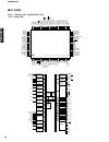
Dsp-ax620 dsp-ax620 29 ■ ic data ic501 : µ pd784217agf (operation p.C.B.) 16 bit µ -com (cpu) 81 82 83 84 85 86 87 88 89 90 91 92 93 94 95 96 97 98 99 100 50 49 48 47 46 45 44 43 42 41 40 39 38 37 36 35 34 33 32 31 1 2 3 4 5 6 7 8 9 10 11 12 13 14 15 16 17 18 19 20 21 22 23 24 25 26 27 28 29 30 80 7...
Page 31
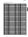
Dsp-ax620 dsp-ax620 30 ic501 : µ pd784217agf (operation p.C.B.) 16 bit µ -com (cpu) no. Port name i/o function o. Port name i/o function 1 p60/a16 ckp o tc74hc164 clock 100 vss mg ground 2 p61/a17 o nc 99 p57/a15 cel o lc78211/lc78213 ce 3 p62/a18 o nc 98 p56/a14 cet o nc 4 p63/a19 o nc 97 p55/a13 s...
Page 32
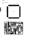
Dsp-ax620 dsp-ax620 31 ic801 : yss928 (dsp p.C.B.) ac3d3 120 11 118 117 116 11 114 113 112 111 110 109 108 59 58 57 56 55 54 53 52 51 50 49 48 47 46 45 44 43 42 41 78 77 80 79 76 75 74 73 72 71 70 69 68 67 66 65 64 63 62 61 60 13 107 14 106 15 105 16 104 17 103 18 102 19 101 20 100 99 98 97 96 95 94...
Page 33
Dsp-ax620 dsp-ax620 32 no. Name i/o function 1 xo o crystal oscillator connecting terminal 2 xi i crystal oscillator connecting terminal (24.576mhz ) 3 seli1 i+ built-in selector input 1 (axd) 4 seli0 i+ built-in selector input 0 (gnd) 5 seloa o+ built-in selector output a (isel) 6 selob o+ built-in...
Page 34
Dsp-ax620 dsp-ax620 33 no. Name i/o function 56 sdwcki1 i+ word clock input terminal for sdib, sdob interface (unconnected) 57 sdbcki1 i+ bit clock input terminal for sdib, sdob interface (unconnected) 58 vss ground terminal 59 sdob3 o pcm output terminal from sub dsp 60 sdob2 o pcm output terminal ...
Page 35
Dsp-ax620 dsp-ax620 34 no. Name i/o function 111 rama5 o sub dsp: external memory address terminal 5 112 rama2 o sub dsp: external memory address terminal 2 113 seli13 i+ built-in selector input 13 (unconnected) 114 seli12 i+ built-in selector input 12 (unconnected) 115 seli11 i+ built-in selector i...
Page 36
Dsp-ax620 dsp-ax620 35 ic587 : lc74781-9798 (operation p.C.B.) superimpose horizontal display position detection horizontal direction character size register horizontal size counter synchronous separation character output dot clock generator synchronous distinction complex synchronous signal separat...
Page 37
Dsp-ax620 dsp-ax620 36 symbol vss1 xtal in xtal out ctrl1 blank osc in osc out chara /cs sclk sin vdd2 cv out nc cv in vdd1 syn in sep c sep out sep in ctrl2 ctrl3 /rst vdd1 pin no. 1 2 3 4 5 6 7 8 9 10 11 12 13 14 15 16 17 18 19 20 21 22 23 24 function connection to gnd (digital system ground termi...
Page 38
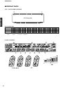
Dsp-ax620 dsp-ax620 37 ■ display data v501 : 10-bt-236gnk (v6785800) pattern area q %5 ● grid assignment note 1) f1, f2 ......... Filament 2) np .............. No pin 3) nc .............. No connction 4) p1~p35 ....... Datum line ● pin connection pin no. 1 2 3 4 5 6 7 8 9 10 11 12 13 14 15 16 17 18 ...
Page 39
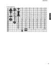
Dsp-ax620 dsp-ax620 38 ● anode connection.
Page 40
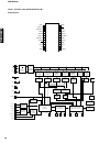
Dsp-ax620 dsp-ax620 39 ● ics njm79m05fa njm79m12fa pq025ez5mzp njm7805fa njm7812fa 1:common 2:input 3:output 3 2 1 1: output 2: common 3: input 3 2 1 tc74hcu04ap tc74hc4053ap 1 7 14 njm2904m-t1 µ pc4570g2 tk15420mtl 1ss133 1t2 1ss270a 1n4002s mtzj4.7c mtzj6.8b mtzj10.0c mtzj12.0c mtzj13.0a mtzj30.0a...
Page 41
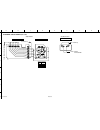
A b c d e f g h 1 2 3 4 5 6 dsp-ax620 e-41/j-39 ■ block diagram phono (l/r) tuner (l/r) cd (l/r) dvd (l/r) d-tv/cbl(l/r) a udio md/cd-r in (l/r) vcr 1 in (l/r) vcr 2/dvr in (l/r) video aux (l/r) md/tape out (l/r) vcr 1 out (l/r) vcr 2/dvr out (l/r) main (l/r) center surround (l/r) subwoofer phono mm...
Page 42
A b c d e f g h 1 2 3 4 5 6 dsp-ax620 ■ block diagram e-42/j-40 dvd d-tv/cbl vcr 1 vcr 2 dvr video aux dvd d-tv/cbl vcr 1 vcr 2 dvr video aux c-input selector ic582 y-input selector ic583 ic588 input selector ic682 ic681b ic681a ic587 q587 ic581a ic585 q585 q584 q581 q586 – 589 ic584a ic581b ic584c ...
Page 43
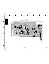
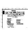
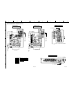
A b c d e f g h 1 2 3 4 5 6 dsp-ax620 ■ printed circuit board (foil side) e-45/j-43 e-44/j-42 ref. No. Location d801 e2 d802 e3 d803 e5 d804 e6 d805 e6 d806 e5 d807 e5 d808 e5 d809 c5 d810 c5 d811 c5 d812 c5 d813 b5 d814 b5 d815 b5 d816 b5 d817 b5 d818 b5 d819 b5 d820 b5 d821 d5 d822 d5 d823 c5 d824...
Page 44
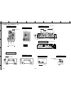
A b c d e f g h 1 2 3 4 5 6 dsp-ax620 ■ printed circuit board (foil side) e-46/j-44 e-47/j-45 ref. No. Location ic301 f3 ic302 f3 ic303 e4 ic304 c3 ● semiconductor location phono cd in out dvd d–tv/cbl in out vcr 1 vcr 2/ dvr in out subwoofer audio output b, g only 11 5 30 16 11 5 30 16 11 5 30 16 1...
Page 45
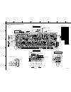
A b c d e f g h 1 2 3 4 5 6 dsp-ax620 ■ printed circuit board (foil side) e-49/j-47 e-48/j-46 input ( 1 ) p. C. B. (surface mount device) 1 4 8 5 1 4 8 5 1 4 8 5 1 4 8 5 1 4 8 5 1 4 8 5 1 4 8 5 1 4 8 5 ref. No. Location ic311 f2 ic313 f3 ic314 d3 ic315 d3 ic316 e4 ic317 b2 ic319 c2 ic320 c2 ● semico...
Page 46
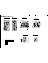
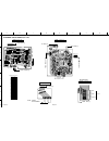
A b c d e f g h 1 2 3 4 5 6 dsp-ax620 ■ printed circuit board (foil side) e-50/j-48 e-51/j-49 ref. No. Location d302 c2 d303 c2 d304 c2 d305 c2 d306 c2 d307 c2 d308 c2 d309 c2 d310 c2 d311 c2 d312 c2 d313 c3 d314 c3 d315 c3 d316 c3 d317 c2 d318 c2 ref. No. Location ic305 c3 ic306 c2 ic307 c2 ic501 g...
Page 47
A b c d e f g h 1 2 3 4 5 6 dsp-ax620 ■ printed circuit board (foil side) e-53/j-51 e-52/j-50 main surr ound center/ subw oofer dv d d – tv/cbl monit or out vcr 1 in out vcr 2/ dv r in out s–video 6ch input 1 8 16 9 1 12 24 13 1 7 14 8 operation ( 2 ) p. C. B. (lead type device) 4 e e e e e e +5v vs...
Page 48
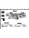
A b c d e f g h 1 2 3 4 5 6 dsp-ax620 ■ printed circuit board (foil side) e-54/j-52 e-55/j-53 ckp ces e/i dest sdrr sdtp sdrp /st int928 mg yssck /icd scn mtc vmt so cet pr v2 lc2 sckr sdtr vsy rdse cep sckp tmt tuned sdd sdm csy dmt mtsw mtmr cev sck cel lc1 from : input (1) volume j, b, g only j o...
Page 49
A b c d e f g h 1 2 3 4 5 6 dsp-ax620 ■ printed circuit board (foil side) e-57/j-55 e-56/j-54 1 30 80 51 31 100 50 81 1 16 17 64 49 48 32 33 j, r, t only b, g only r, t only r, t, b, g only b, g only j, r, t only operation ( 1 ) p. C. B. (surface mount device) dv d d – tv/cbl in out vcr 1 vcr 2 /d v...
Page 50
A b c d e f g h 1 2 3 4 5 6 dsp-ax620 ■ printed circuit board (foil side) e-58/j-56 e-59/j-57 monit or out d – tv/cbl dv d component video 1 8 16 9 cmp1 cmp0 +5v – 5v to : ope (3) w711 operation ( 5 ) p. C. B. (lead type device) 18 16 9 operation ( 5 ) p. C. B. (surface mount device) optical video s...
Page 51
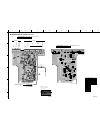
A b c d e f g h 1 2 3 4 5 6 dsp-ax620 ■ printed circuit board (foil side) e-61/j-59 e-60/j-58 ref. No. Location d101 e3 d102 e3 d103 d3 d104 c3 d105 b3 d106 d2 d107 d2 d108 e3 d109 e3 d110 d3 d111 c3 d112 b3 d113 f2 d114 f2 d115 f2 d116 e2 d117 f2 d118 c2 d119 b2 d120 f2 d121 f3 d122 f3 d123 f2 d124...
Page 52
A b c d e f g h 1 2 3 4 5 6 dsp-ax620 ■ printed circuit board (foil side) e-62/j-60 e-63/j-61 e +b bv vc nfc vrr nfrr vrl nfrl vr nfr vl nfl – bv from : main (1) e e e e lc2 –12 +12 lc1 +5d l r rl rr c +25 –25 –5 +5 fr om : input (1) main ( 2 ) p. C. B. – 12 +12 – 5 +5 +5d – 25 +25 from : power (3) ...
Page 53
A b c d e f g h 1 2 3 4 5 6 dsp-ax620 ■ printed circuit board (foil side) e-65/j-63 e-64/j-62 +dg +b3 – b2 e +b2 – b4 +b4 power ( 2 ) p. C. B. To : power (3) from : power transformer ac3 ac3 ac2 e ac2 w722 bl power ( 3 ) p. C. B. –12 +12 –5 +5 +5d –12 +12 from : main (6) dg +b3 – b2 e +b2 – b4 +b4 t...
Page 54
A b c d e f g h 1 2 3 4 5 6 dsp-ax620 ■ printed circuit board (foil side) e-66/j-64 e-67/j-65 to : power (1) fr om : po wer transformer power ( 4 ) p. C. B. ● r, t models power ( 6 ) p. C. B. Br br be wh or ye re gy be or br re wh ye voltage selector 240v 220v 110v 120v 1 − 2/5 − 6 2 − 3/6 − 7 3 − 4...
Page 55
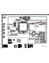
A b c d e f g h 1 2 3 4 5 6 i j k l m n 7 8 9 10 dsp-ax620 ■ schematic diagram (dsp) * all voltage are measured with a 10m Ω /v dc electric volt meter. * components having special characteristics are marked z and must be replaced with parts having specifications equal to those originally installed. ...
Page 56
A b c d e f g h 1 2 3 4 5 6 i j k l m n o 7 8 9 10 dsp-ax620 ■ schematic diagram (input 1/2) * all voltage are measured with a 10m Ω /v dc electric volt meter. * components having special characteristics are marked z and must be replaced with parts having specifications equal to those originally ins...
Page 57
A b c d e f g h 1 2 3 4 5 6 i j k l m n 7 8 9 10 dsp-ax620 ■ schematic diagram (input 2/2 & operation 1/2) * all voltage are measured with a 10m Ω /v dc electric volt meter. * components having special characteristics are marked z and must be replaced with parts having specifications equal to those ...
Page 58
A b c d e f g h 1 2 3 4 5 6 i j k l m n o 7 8 9 10 dsp-ax620 ■ schematic diagram (operation 2/2) * all voltage are measured with a 10m Ω /v dc electric volt meter. * components having special characteristics are marked z and must be replaced with parts having specifications equal to those originally...
Page 59
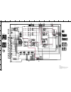
A b c d e f g h 1 2 3 4 5 6 i j k l m n 7 8 9 10 dsp-ax620 ■ schematic diagram (main 1/2) * all voltage are measured with a 10m Ω /v dc electric volt meter. * components having special characteristics are marked z and must be replaced with parts having specifications equal to those originally instal...
Page 60
A b c d e f g h 1 2 3 4 5 6 i j k l m n o 7 8 9 10 dsp-ax620 ■ schematic diagram (main 2/2 & power) * all voltage are measured with a 10m Ω /v dc electric volt meter. * components having special characteristics are marked z and must be replaced with parts having specifications equal to those origina...
Page 61: Parts List
Dsp-ax620 dsp-ax620 74 abbreviations in this list are as follows : c.A.El.Chp : chip alumi. Electrolytic cap c.Ce : ceramic cap c.Ce.Array : ceramic cap array c.Ce.Chp : chip ceramic cap c.Ce.Ml : multilayer ceramic cap c.Ce.M.Chp : chip multilayer ceramic cap c.Ce.Safty : recognized ceramic cap c.C...
Page 62
Dsp-ax620 dsp-ax620 75 p.C.B. Input schm ref. Part no. Description market new parts * schm ref. Part no. Description market new parts * * v7209300 p.C.B. Input rt * v7209400 p.C.B. Input bg cb301 vi878100 cn.Bs.Pin 3p cb302 vp082900 cn.Bs.Pin 25p * cb303 vq048600 cn 37p te cb304 vq047800 cn.Bs.Pin 2...
Page 63
Dsp-ax620 dsp-ax620 76 p.C.B. Input schm ref. Part no. Description market new parts * schm ref. Part no. Description market new parts * c428 uu137100 c.El 10uf 16v c429 uu137100 c.El 10uf 16v c430 ur837100 c.El 10uf 16v c431 ua652100 c.Mylar 100pf 50v c432 ua652100 c.Mylar 100pf 50v c433 ur837100 c....
Page 64
Dsp-ax620 dsp-ax620 77 p.C.B. Input & operation schm ref. Part no. Description market new parts * schm ref. Part no. Description market new parts * r402 vp940200 r.Mtl.Oxd 47Ω 1w r403 vp940200 r.Mtl.Oxd 47Ω 1w r404 vp940200 r.Mtl.Oxd 47Ω 1w r405 hv754100 r.Car.Fp 10Ω 1/4w r457 vp940200 r.Mtl.Oxd 47Ω...
Page 65
Dsp-ax620 dsp-ax620 78 p.C.B. Operation schm ref. Part no. Description market new parts * schm ref. Part no. Description market new parts * c629 us062470 c.Ce.M.Chp 470pf 50v c630 ur866100 c.El 1uf 50v c631 us061240 c.Ce.Chp 24pf 50v c632 us061240 c.Ce.Chp 24pf 50v c633 us062220 c.Ce.Chp 220pf 50v c...
Page 66
Dsp-ax620 dsp-ax620 79 p.C.B. Operation & dsp schm ref. Part no. Description market new parts * schm ref. Part no. Description market new parts * q503 vv900500 tr 2sd1991a q,r,s q504 ia093320 tr 2sa933s q,r q505 ia093320 tr 2sa933s q,r q506 ia093320 tr 2sa933s q,r q507 vv900500 tr 2sd1991a q,r,s q50...
Page 67
Dsp-ax620 dsp-ax620 80 p.C.B. Dsp schm ref. Part no. Description market new parts * schm ref. Part no. Description market new parts * c864 us135100 c.Ce.Chp 0.1uf 16v c865 ur818100 c.El 100uf 6.3v c866 us135100 c.Ce.Chp 0.1uf 16v c867 us135100 c.Ce.Chp 0.1uf 16v c868 us135100 c.Ce.Chp 0.1uf 16v c869...
Page 68
Dsp-ax620 dsp-ax620 81 p.C.B. Dsp & main schm ref. Part no. Description market new parts * schm ref. Part no. Description market new parts * d808 vt332900 diode 1ss355 d809 vt332900 diode 1ss355 d810 vt332900 diode 1ss355 d811 vt332900 diode 1ss355 d812 vt332900 diode 1ss355 d813 vt332900 diode 1ss3...
Page 69
Dsp-ax620 dsp-ax620 82 p.C.B. Main schm ref. Part no. Description market new parts * schm ref. Part no. Description market new parts * c113 vr325000 c.Mylar 100pf 100v c114 vr325000 c.Mylar 100pf 100v c115 vg287500 c.El 47uf 50v c116 vr325000 c.Mylar 100pf 100v c117 vr325000 c.Mylar 100pf 100v c118 ...
Page 70
Dsp-ax620 dsp-ax620 83 p.C.B. Main schm ref. Part no. Description market new parts * schm ref. Part no. Description market new parts * d111 vn008700 diode 1ss270a d112 vn008700 diode 1ss270a d113 vd631600 diode 1ss133,176 d114 vd631600 diode 1ss133,176 d115 vg440300 diode.Zenr mtzj12c 12v d116 vg440...
Page 71
Dsp-ax620 dsp-ax620 84 p.C.B. Main schm ref. Part no. Description market new parts * schm ref. Part no. Description market new parts * r110 v3946100 r.Mtl.Oxd 2.7kΩ 0.5w r111 v3945100 r.Mtl.Oxd 390Ω 0.5w r112 v3945600 r.Mtl.Oxd 1kΩ 0.5w r113 v3945500 r.Mtl.Oxd 820Ω 0.5w r115 vp941600 r.Mtl.Oxd 5.6kΩ...
Page 72
Dsp-ax620 dsp-ax620 85 p.C.B. Power schm ref. Part no. Description market new parts * schm ref. Part no. Description market new parts * * v7210200 p.C.B. Power rt * v7210400 p.C.B. Power b * v7210500 p.C.B. Power g cb701 vq962800 cn.Bs.Pin 7p cb702 vi878500 cn.Bs.Pin 7p cb721 vi878500 cn.Bs.Pin 7p c...
Page 73
Dsp-ax620 86 87 chip resistor schm ref. Part no. Description market new parts * schm ref. Part no. Description market new parts * rd350000 r.Car.Chp 0Ω 1/10w rd353100 r.Car.Chp 1Ω 1/10w rd353220 r.Car.Chp 2.2Ω 1/10w * rd353470 r.Car.Chp 4.7Ω 1/16w rd354330 r.Car.Chp 33Ω 1/10w rd354470 r.Car.Chp 47Ω ...
Page 74
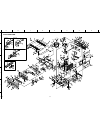
A b c d e f g h 1 2 3 4 5 6 dsp-ax620 ■ exploded view 88 89 g model r,t models b model 1-12 163 160 160 121 122 1-5 1-11 1-13 1-10 1-7 1-6 1-25 1-25 1-40 1-25 1-3 1-25 6 (7) 1-25 6 (4) 6 (1) 6 (8) 1-25 7 (3) 124 10 (4) 6 (9) 10 (6) 9 (5) 9 (6) 15 170 9 (2) 163 120 102 163 120 138 135 135 135 135 1-1...
Page 75
Dsp-ax620 dsp-ax620 90 ref. No. Part no. Description remarks markets new parts * * 1‑3 v7331800 s flexible flat cable 37p 250mm p=1.25 * 1‑5 v6871600 front panel bl * 1‑5 v6871700 front panel gd * 1‑5 v6871800 front panel ti * 1‑6 v6921900 sub panel bl * 1‑6 v6922000 sub panel gd * 1‑6 v6922100 sub ...
Page 76
Dsp-ax620 dsp-ax620 91 ref. No. Part no. Description remarks markets new parts * z 16 vz542500 power cord ass'y rt 17 v2438700 cord stopper 10p1 * 25 mf118200 flexible flat cable 18p 200mm 26 mf125100 flexible flat cable 25p 100mm 27 mf227160 s flexible flat cable 27p 160mm * 101 v7558900 top cover ...
Page 77
Dsp-ax620 dsp-ax620 92 ref. No. Part no. Description remarks markets new parts * 171 vh313200 bw head s‑tite screw 4x8‑10 fnm3‑bl ti 176 aa627310 ground terminal accessories * 200 v6941100 remote control transmitter rav214 rt * 200 v6941200 remote control transmitter rav215 bg 200‑1 aax14030 lid bw0...
Page 78: Remote Control Transmitter
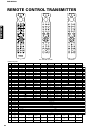
Dsp-ax620 dsp-ax620 93 remote control transmitter a/b/c/d/e 7a15 7a16 7ac9 7ac1 7a54 7a0f 7a14 7a55 7a13 7aca 7a87 7a18 7a11 7a10 7a85 7a98 7a12 7a53 7ac2 7a86 x x 7a1e 7a57 7a1c only "amp/tuner" 0003 code 7a1d 7a1a 7a1b 7a9c 7a52 x x x 3 4 5 6 7 8 9 10 11 12 13 16 15 14 26 27 28 32 33 34 29 key pos...
Page 79
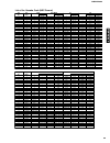
Dsp-ax620 dsp-ax620 94 key key dvd dvd menu ld cd no. Name yamaha 0008 yamaha 0008 yamaha 0007 yamaha 0005 yamaha 0015 3 1 1 7c-94 1 7c-94 1 7c-17 1 79-11 79-11 4 2 2 7c-95 2 7c-95 2 7c-18 2 79-12 79-12 5 3 3 7c-96 3 7c-96 3 7c-19 3 79-13 79-13 6 4 4 7c-97 4 7c-97 4 7c-1a 4 79-14 79-14 7 5 5 7c-98 5...
Page 80
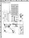
A b c d e 1 2 3 4 5 6 7 dsp-ax620 95 ■ schematic diagram k41 k42 k43 k44 k45 k46 k33 k34 k35 k36 k37 k38 k25 k26 k27 k28 k29 k30 k17 k18 k19 k20 k21 k22 k9 k10 k11 k12 k13 k14 k1 k2 k3 k4 k5 k6 vba t vba t vba t vdd vdd vdd q1 ba tt vdd c1 c12 c2 c3 c4 option option option x1 35 38 9 42 41 40 39 34 ...
Page 81
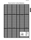
Parts list for carbon resistors 1/6w type part no. Hf45 7100 hf45 7110 hf85 7120 hf45 7130 hf45 7150 hf45 7180 hf45 7220 hf45 7240 hf85 7270 hf45 7300 hf45 7330 hf45 7360 hf45 7390 hf45 7470 hf45 7510 hf45 7560 hf45 7620 hf45 7680 hf45 7820 hf45 7910 hf45 8100 hf45 8110 hf45 8120 hf45 8150 hf45 8180...
Page 82: Dsp-Ax620
Dsp-ax620 dsp-ax620

