- DL manuals
- Zarlink
- Motherboard
- Le51HE0060V2
- User Manual
Zarlink Le51HE0060V2 User Manual
Summary of Le51HE0060V2
Page 1
Le51he0060v2 le58ql063 qlslac™ / le5711/12 dslic™ evaluation board user’s guide rev. A, ver. 2 october 2, 2007 document number: 081167.
Page 2
Www.Zarlink.Com information relating to products and services furnished herein by zarlink semiconductor inc. Or its subsidiaries (collectively “zarlink”) is believed to be reliable. However, zarlink a ssumes n o liability f or errors t hat may a ppear in t his pu blication, or f or lia bility o ther...
Page 3: Table of Contents
I zarlink semiconductor inc. Document id# 081167 date: oct 2, 2007 rev: a version: 2 distribution: public document table of contents chapter 1 introduction . . . . . . . . . . . . . . . . . . . . . . . . . . . . . . . . . . . . . . . . . . . . . . . . . . . . . . . . . . . . . . 1 1.1 overview . . ....
Page 4
Le51he0060v2 eval board user guide ii zarlink semiconductor inc..
Page 5: Introduction
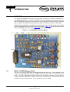
Chapter 1 zarlink semiconductor inc. 1 introduction 1.1 overview the zarlink le51he0060v2 evaluation board provides a platform to evaluate the capabilities of the le58ql063 qlslac™ and le5711/12 dslic™ devices. All digital control signals, voice band and mpi signals have test points for easy probing...
Page 6
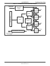
Le51he0060v2 eval board user guide 2 zarlink semiconductor inc. Figure 1–2 le51he0060v2 evaluation board block diagram qslac dslic dslic channel 1 interface (emr) channel 2 interface (emr) channel 3 interface (lcas) channel 4 interface (lcas) ringing voltage distribution circuits power distribution ...
Page 7: Board Setup and Con-
Chapter 3 zarlink semiconductor inc. 2 board setup and con- nection 2.1 board features the le51he0060v2 evaluation board design features the following: • mpi/pcm connector • tip/ring banana jacks and rj-11 connectors • test points for all major signals • banana jacks for all power connections • qsla...
Page 8
Le51he0060v2 eval board user guide 4 zarlink semiconductor inc. 2.2 board connections the le51he0060v2 can be plugged directly into either a voice path demo (vp demo) board or an advanced computer interface board (acif2-a) via the 50-pin ifb01 connector of the le51he0060v2 evaluation board. All powe...
Page 9
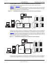
Le51he0060v2 eval board user guide 5 zarlink semiconductor inc. 2.3 interconnection of the le51he0060v2 evaluation board a representative connection of a complete zarlink evaluation platform setup is shown in figure 2–1 and figure 2–2 below. Figure 2–1 shows the evaluation board connected to the 50-...
Page 10
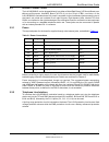
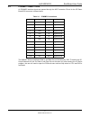
Le51he0060v2 eval board user guide 6 zarlink semiconductor inc. 2.4 pcm/mpi connections all pcm/mpi interface signals are passed through the acif connector. Pinout for the vp demo board spa connector is shown below. The qlslac device multiplexes data in and data out on the same pin, dio. To assure t...
Page 11: Board Operation
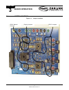
Chapter 7 zarlink semiconductor inc. 3 board operation 3.1 jumper locations figure 3–1 jumper locations dslic jumpers ringing jumpers dslic manual controls.
Page 12
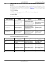
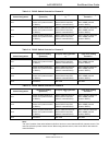
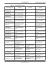
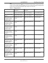
Le51he0060v2 eval board user guide 8 zarlink semiconductor inc. 3.2 jumper and switch settings for the le51he0060v2 evaluation board this evaluation board contains a plethora of jumper and switch settings to allow testing of all the operational modes of the qlslac/dslic combination. Figure 3–1 shows...
Page 13
Le51he0060v2 eval board user guide 9 zarlink semiconductor inc. Note: the "open" position of the switch allows the qlslac device to control the three dslic channel controls. The other two positions provide manual control. When using manual controls, refer to the dslic data sheet for state informatio...
Page 14
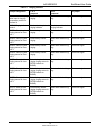
Le51he0060v2 eval board user guide 10 zarlink semiconductor inc. Table 3–6 line side dslic controls jumper designation 1 to 2 jumpered 2 to 3 jumpered no jumper j5, intended for troubleshooting and insertion of ammeter in line. Ring3 - lcas and output jacks connected to dslic n/a ring3 lcas and outp...
Page 15
Le51he0060v2 eval board user guide 11 zarlink semiconductor inc. Note: all of the jumpers in the table below must be set consistently for proper operation. All jumpers must connect positions 1 and 2 for battery-backed ringing or connect 2 and 3 for earth-backed ringing. The setting of these jumpers ...
Page 16
Le51he0060v2 eval board user guide 12 zarlink semiconductor inc. Jsr12, dslic db2 (neg- ative input for ring trip comparator) control for channel 4. Select battery backed ringing. Select earth backed ring- ing. Disconnect signal. Jsr13, ringing indicator control. Illuminate battery backed ringing in...
Page 17: Software Operation
Chapter 13 zarlink semiconductor inc. 4 software operation 4.1 overview three software platforms enable the user full control of the le51he0060v2 evaluation board. The first two are control platforms to communicate with the evaluation board. The first platform is the vp demo board and the vp-script ...
Page 18
Le51he0060v2 eval board user guide 14 zarlink semiconductor inc..
Page 19: Schematics
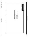
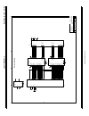
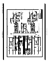
Chapter 15 zarlink semiconductor inc. 5 schematics 5.1 evaluation board schematics schematics and a bill of materials for the le51he0060v2 evaluation board are included on the following pages..
Page 20
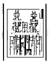
Le51he0060v2 eva l board user gu ide 16 z arlink semicon ductor inc. 5 5 4 4 3 3 2 2 1 1 d d c c b b a a p a ge 1 cover sheet page 2 bl ock schematic page 3 ds lic 1 schematic page 4 ds lic 2 schematic page 5 power and decoulping schematic page 6 qslac sc hematic page 7 ring signal schematic 5 8 q l...
Page 21
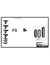
Le51he0060v2 e val boar d user guide 17 z arlink semicon ductor inc. 5 5 4 4 3 3 2 2 1 1 d d c c b b a a page 7 page 2 page 3 page 4 page 6 page 5 hierarchical flow le51he0060v 2 2 .0 z zarlink qlslac dslic 5712 evaluation board c 27 friday, june 20, 2003 wp e ppc - vna 2136 north 1 3th st readi ng,...
Page 22
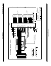
Le51he0060v2 e val boar d user guide 18 z arlink semicon ductor inc. 5 5 4 4 3 3 2 2 1 1 d d c c b b a a ring2 red tip2 black tip1 black ring1 red dslic channels 1 & 2 with emr see note 1. See note 1. Notes: 1. Board m a y b e assembled with either ptc's or resistors tx2-5v tx2-5v 2. Due to socket d...
Page 23
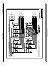
Le51he0060v2 e val boar d user guide 19 z arlink semicon ductor inc. 5 5 4 4 3 3 2 2 1 1 d d c c b b a a ring3 red tip3 black dslic channels 3 & 4 with lcas s e e note 1. See n ote 1. (p la c e 0 ohm jumper within outline of rs-2b res is to r. ) (p la c e 0 ohm jumper within outline of rs-2b res is ...
Page 24
5 5 4 4 3 3 2 2 1 1 d d c c b b a a power & decoupling bgnd agnd dgnd +5v +3.3v vbat2 vbat1 do not populate socketed le51he0060v2 2.0z zarlink qlslac dslic 5712 evaluation board b 5 7 wednesday, may 28, 2003 wpe ppc - vna 2136 north 13th st reading, pa 19604 title size document number rev date: shee...
Page 25
Le51he0060v2 eval board user guide 21 zarlink semiconductor inc..
Page 26
Le51he0060v2 eva l board user gu ide 22 z arlink semicon ductor inc. 5 5 4 4 3 3 2 2 1 1 d d c c b b a a to dslic1 to dslic2 qlslac & pcm/mpi connections page 3 page 4 to dslic 1 & 2 diagrams pin 1 - 2 = mclk inp u t to qlslac pin 2 - 3 = e 1 output to dslic to metering diagram socket e d le51he0060...
Page 27
Le51he0060v2 e val boar d user guide 23 z arlink semicon ductor inc. 5 5 4 4 3 3 2 2 1 1 d d c c b b a a ring i n channel 1 & 2 channel 3 & 4 battery backed ringing channel 3 & 4 channel 1 & 2 (off board ringing signal) rin g r e turn earth backed ringing notes: 1). Jumpers js3 through js9 are a sin...
Page 28
Le51he0060v2 e val boar d user guide 24 z arlink semicon ductor inc. 4.2 l e51he0060v2 bill of materials item quantity reference part foot print manufacturer part number distributor distributor part number tolerance voltage notes 1 115 vtx1,vrx1,vref1,tip1, t p sip-1p keystone 5013 digikey 5013k-nd ...
Page 29
Le51he0060v2 e val boar d user guide 25 z arlink semicon ductor inc. Le51he0060v2 bill of materials (cont.) 22 8 rled1,ldet1,rled2,ldet2, 5372t5 2pin chicago miniture lamp 5372t5-5vlc digikey l20295-nd 5 v ldet3,ldet4,d11,d12 23 4 tc1,tc3,ec4,ec5 10uf f_case_code panasonic ece-v2aa100p digikey pce32...
Page 30
Le51he0060v2 e val boar d user guide 26 z arlink semicon ductor inc. Le51he0060v2 bill of materials (cont.) p2-26,p2-27,p2-28,p2-29, p2-30,p2-31,p2-32,p2-33, p2-34,p2-35,p2-36,p2-37, p2-38,p2-39,p2-40,p2-41, p2-42,p2-43,p2-44,p2-45, p2-46,p2-47,p2-48,p2-49, p2-50,p2-51,p2-52,p2-53, p2-54,p2-55,p2-56...
Page 31
Le51he0060v2 e val boar d user guide 27 z arlink semicon ductor inc. Le71he00602v bill of materials (cont.) 55 4 rr1,rr2,rr3,rr4 400 x2w vishay cpf2-400-f mouser 71-cpf2-f-400 1% 56 8 rtb1,rta1,rtb2,rta2,rtb3, 49.9k x1/4w vishay cmf-4992f m ouser 71rn60d-f-4992 1 % rta3,rtb4,rta4 57 2 rth1,rth3 1.8m...
Page 32: Glossary
Appendix glossary 27 a glossary the following is a list of terms and their definitions, as used in this manual. Acif2-a advanced computer interface board second design, revision a. This board works with the winacif software program and is used as an interface between the host pc and evaluation board...

