- DL manuals
- Zenith
- DVD Player
- DVB352
- Service Manual
Zenith DVB352 Service Manual
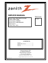
SERVICE MANUAL
Product Type: DVD VIDEO PLAYER
Chassis: DPM-4 (MD)
Manual Series: DVB352
Manual Part #: 3829RGN002K
Model Line: D
Product Year: 2003
Summary
1
Cabinet & Main Chassis
2
Electrical
3
Parts List
4
Published September 2003
by Technical Publications
Zenith Electronics Corporation
201 James Record Road
Huntsville, Alabama 35824-1513
Copyright © 2003 by Zenith Electronics Corporation
Printed in U.S.A
Model Series:
CONTENTS
DVB352
....................................................
.............................
....................................................
....................................................
Summary of DVB352
Page 1
Service manual product type: dvd video player chassis: dpm-4 (md) manual series: dvb352 manual part #: 3829rgn002k model line: d product year: 2003 summary 1 cabinet & main chassis 2 electrical 3 parts list 4 published september 2003 by technical publications zenith electronics corporation 201 james...
Page 3: Section 1
1-1 section 1 summary contents product safety servicing guidelines for video products ............. 1-2 servicing precautions .................................................................................................. 1-3 • general servicing precautions • insulation checking prodedure • elect...
Page 4
1-2 1-3 important safety notice this manual was prepared for use only by properly trained audio-video service technicians. When servicing this product, under no circumstances should the original design be modified or altered without permission from zenith electronics corporation. All components shou...
Page 5: Servicing Precautions
1-3 servicing precautions caution : before servicing the dvd covered by this service data and its supplements and addends, read and follow the safety precautions. Note : if unforeseen circum- stances create conflict between the following servicing pre- cautions and any of the safety precautions in t...
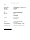
Page 6: Specifications
1-4 specifications • general power requirements ac 120 v, 60 hz power consumption 14w dimensions (approx.) 440 x 80 x 425 mm (17.3 x 3.1 x 16.7 inches) (w x h x d) weight (approx.) 5.1 kg (11.2 lbs) operating temperature 5˚c to 35˚c (41˚f to 95˚f) operating humidity 5 % to 90 % • system laser semico...
Page 7: Section 2
2-1 section 2 cabinet & main chassis contents 1. Exploded views ................................................................................................................2-2 1. Cabinet and main frame section .........................................................................................
Page 8: Exploded Views
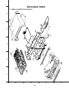
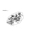
2-2 exploded views 1. Cabinet and main frame section 465 465 250 462 462 300 dig901 465 261 260 275 463 463 465 467 463 463 463 a00 a47 a46 a48 a43 a42 a49 283 280 452 452 320 261a 261a a 5 4 3 2 1 b c d.
Page 9
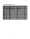
2-3 • cabinet and main frame section • cabinet and main frame section part list s al loca no lg part no a description specification remarks assembly parts section a42 6871r-5097a o pwb(pcb) assembly,total dm6000 sh key1 a43 3501rf4030l o board assembly dvd dm7912nm ha1uzz front a46 6885r-0700a o sub...
Page 10
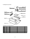
2. Packing accessory section battery 808 packing sheet 804 packing 803 811 812 owner's manual plug ass'y 1way(yellow) plug ass'y 2way 810 cable set ass'y 801 remocon 900 box carton 802 packing 803 806 cable, din 2-4 • packing accessory section part list s al loca no lg part no a description specific...
Page 11: Section 3
3-1 section 3 electrical contents electrical troubleshooting guide ......................................................................3-2 1. Power check flow.....................................................................................................................3-2 2. System operation...
Page 12
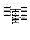
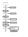
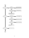
3-2 electrical troubleshooting guide no 5v_a . No 5.2va. Is 5.2va section working? Is 5.2v present at emitter of q107? Replace q107. Is there a dc voltage at (+) terminal of bd101? Is there a dc voltage at r101? Replace ic101. Check f101 1. Power check flow no vf+ is 5.2va section working? Replace d...
Page 13
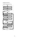
3-3 2. System operation flow power on no yes yes no no show logo tray closed? Tray close to closed position judge whether have disc in 5 tray recieve open/ close key? Receive close key? 1. Stop playback & open tray 2. Display tray open message & logo 1. Execute pressed key & ir key 2. Systemoperati ...
Page 14
3-4 3. Test & debug flow test check the power part no yes no yes no no no yes yes check the power part check the regulators or diode( d670). Check the cable connection front panel & communication signal 1. Check 27mhz system clock. 2. Check systemreset circuit. 3. Check flash r/wenable signal prd, r...
Page 15
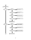
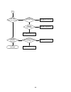
3-5 a b reset or power on. Show logo? Flash memory operates properly? Check connecti on lines between flash & mt1379 and the flash access time whether is sui table or not. Sdram works properl y? Mt1379 video outputs properly? Have tv signal output? Check av cable connection to tv set . Check the loa...
Page 16
3-6 b no yes yes yes no yes yes yes no yes no no no does the sled move to inner side when it is at outter positi on? Motor driver stby pin is high? Motor driver stby pin is high? Sl+ and sl- output properl y? Optical lens has movements for searching focus? Proper f+ & f- outputs? Check cable connect...
Page 17
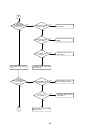
3-7 c no no no no no no no yes yes yes yes yes yes yes yes yes no no laser turns on when reading disc? Ld01 or ld02 output properly? Check the laser power circuit on mt1336 and connecting to power transistor. (q204, q205) check therel ated ci rcuit on laser power transi stor check the related circui...
Page 18
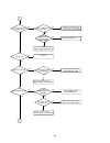
3-8 d yes yes no no yes yes yes yes yes yes yes no no no no no focus on ok? Track on ok? Disc is play? E proper signals on a, b, c, d of mt1336 check connections between mt1336 and pick-up head. Proper feo signal on mt1336? Proper feo signal on mt1336? Check the related circuit on mt1336 feo sugnal ...
Page 19
3-9 e normal audio output when disc playback? Normal ir. Vfd & front pannel key functions? Test end audio dac received correct data stream? Normal audio dac out? (ic601) check audio filter, amplify, mute circuit. (ic602 application circuit)? Check the cable connection on front pannel. Check connecti...
Page 20
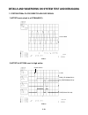
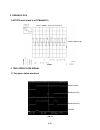
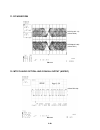
Details and waveforms on system test and debugging 1. System 27mhz clock,reset,flash r/w signal 1) mt1379 main clock is at 27mhz(x501) 3.8v, 27mhz fig 1-1 2) mt1379 & mt1336 reset is high active. Pwr_ctl(cn505 pin 7) 5.2va power cord in m_reset(cn505 pin 9) urst(ic501 pin 188) fig 1-2 3-10
Page 21
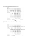
3-11 3) rs232 waveform during procedure(downloading) txd(j6 pin3) rxd(j6 pin 2) fig 1-3 4) flash r/w enable signal during download(downloading) frd(ic5a1 pin 28) fwr(ic5a1 pin 11) fig 1-4.
Page 22
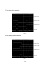
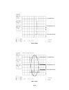
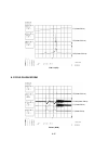
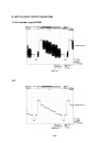
3-12 2. Sdram clock 1) mt1379 main clock is at 27mhz(x501) (ic502,ic503 pin 35) dclk = 93mhz, vp-p=2.2, vmax=2.7v fig 2-1 3. Tray open/close signal 1) tray open status waveform mode1(open) mode2(close) mode3(check) tropen fig 3-1.
Page 23
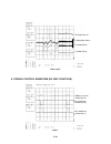
3-13 2) tray close status waveform mode1(open) mode2(close) mode3(check) tropen fig 3-2 3) tray exchage status waveform mode1(open) mode2(close) mode3(check) tropen fig 3-3.
Page 24
3-14 4. Sled control related signal (no disc condition) fmso(2.0v/1.4v/1.0v) (ic501 pin 19) stby(5v) – (ic201 pin 50) sl+(4.7v/3.6v/1.9v) (ic202 pin 12) sl-(5.3v/3.7v/2.5v) (ic202 pin 13) fig 4-1 5. Lens control related signal(no disc condition) foso(1.5v/1.4v/1.3v) (ic501 pin 12) f+(4.0v/3.6v/3.2v)...
Page 25
3-15 6. Laser power control related signal(no disc condition) mdi1(0v/180mv) (ic201 pin 124) ld01(5.0v//3.5v) ic201 pin 125) ld02(5.0v/3.6v) (ic201 pin 126) fig 6-1 7. Disc type judgement waveform f+(ic202 pin 9) fe(ic201 pin 18) rfl(ic201 pin 19) fig 7-1 (dvd).
Page 26
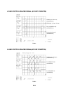
3-16 f+(ic202 pin 9) fe(ic201 pin 18) rfl(ic201 pin 19) fig 7-2 (dvd) f+(ic202 pin 9) fe(ic201 pin 18) rfl(ic201 pin 19) fig 7-3 (cd).
Page 27
3-17 f+(ic202 pin 9) fe(ic201 pin 18) rfl(ic201 pin 19) fig 7-4 (cd) 8. Focus on waveform fe(ic201 pin 18) foso(ic501 pin12) f+(ic202 pin 9) f-(ic202 pin 8) fig 8-1 (dvd).
Page 28
3-18 fe(ic201 pin 18) foso(ic501 pin12) f+(ic202 pin 9) f-(ic202 pin 8) fig 8-2 (cd) 9. Spindle control waveform (no disc condition) dmso(1.4v/1.8v) (ic501 pin 18) sp-(3.6v/2.4v) (ic202 pin 10) sp+(3.6v/4.8v) (ic202 pin 11) fig 9-1.
Page 29
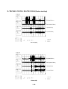
3-19 10. Tracking control related signal(system checking) te(ic201 pin 21) trso(ic501 pin 13) t-(ic202 pin 7) t+(ic202 pin 6) fig 10-1(dvd) te(ic201 pin 21) trso(ic501 pin 13) t-(ic202 pin 7) t+(ic202 pin 6) fig 10-2(cd).
Page 30
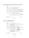
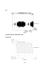
3-20 11. Rf waveform rfop(2.3v/1.1v) (ic201 pin 6) rfon(0.8v/2.0v) (ic201 pin 7) fig 11-1 12. Mt1379 audio optical and coaxial output (aspdif) (ic501 pin 153) fig 12-1.
Page 31
3-21 13. Mt1379 video output waveform 1) full colorbar signal(cvbs) (ic604 pin 23) dclk = 93mhz, vp-p=2.2, vmax=2.7v fig 13-1 2) y (ic604 pin 21) fig 13-2.
Page 32
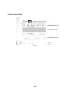
3-22 3) c (ic604 pin 26) dclk = 93mhz, vp-p=2.2, vmax=2.7v fig 13-3 14. Audio output from audio dac 1) audio l/r fig 14-1 (jk601 pin 4,5).
Page 33
3-23 2) audio related signal asdat3(ic501 pin 157) abck(ic501 pin 148) alrck(ic501 pin 149) asdata3 fig 14-2.
Page 34: Block Diagrams
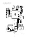
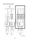
3-24 block diagrams 1. Overall block diagram m m disc spindl e mo to r lo a d ing mo t o r deck mechanism dv d: rf 0 ,a ,b, c, d c d :r f0 ,a,b ,c ,d ,e, f pick up dig901 fld displ a y key in p u t 6m hz x-ta l b/pb ic5 a 1 29lv800t a -70 1m 8bit fl a s h rom urst a[00 :1 9] pc e# pr d # pw r # dq[0...
Page 35
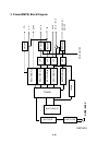
3-25 2. Power(smps) block diagram 5v_ a / 5v_d -29va vf+ rectifier line filter switching ic trans feed b. Reg(8v) 8v 5.2va vf- rectifier(fld ) rectifier(9v) rectifier(5.2v) lpf lpf rectifier(14v) lpf 12 v_a ac90~240v pwr on/off reg(3.3v) 3.3v/3.3v_m / 3.3v_m1 reg(12v ) on/of f rectifier(3.8v) lpf dm...
Page 36
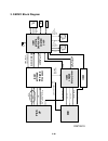
3-26 ic202 ic202 la6560 motor driver dvd: a,b,c,d, rfo cd: a,b,c,d, e, f,rfo sp+, sp - m/ d pick up x501 ic501 mt1379 dvdplayer combo chip ic201 mt1336e rf signa l processor foso,trso,fmso dmso,,tropen feo,teo,rfl,rfrp bdo,cso,htrc,v2p8 adi n f+, f-, t +, t - sl+ , sl - turn_m+,turn_m- turn_m+,turn_...
Page 37
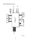
3-27 4. Mpeg & memory block diagram ic503 sdra m 16 m ic505 eepro m iic 501 (mpeg + dsp ) mt1379 ic5a 1 flash memory (8 m ) ic510 (74hct244 ) voltage level shift video int e rface audio int erface rf ic int erface front mi co m in te rfa c e (f r o n t b o a r d ) ic502 sdra m 16 m rfop,rfon,htrc,rf...
Page 38
3-28 5. Video & audio block diagram ic604 video 6db am p ic601 audio dac (2ch) ic301 audio dac (5.1ch) ic602 (op amp) lpf&buffer ic302 (op amp) lpf&buffer ic303 (op amp) lpf&buffer ic304 (op amp) lpf&buffer cvbs component (r.G.B) / (y.Pb.Pr ) super video (y/c) (r.G.B) / (y.Pb.Pr ) (y/c) dac reset ac...
Page 40
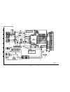
3-29 3-30 circuit diagrams 1. Power(smps) circuit diagram important safety notice when servicing this chassis, under no cir- cumstances should the original design be modified or altered without permission from the zenith electronics corporation. All components should be replaced only with types iden...
Page 41
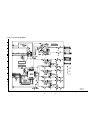
3-31 3-32 program download fail no power on digitron all not display system not working system not working or screen is abnormal system not working or digitron not display system not operate sr5850a dm7912n video signal y video signal color audio dac interface video interface rf & motor drive interf...
Page 42
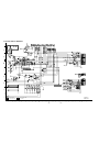
3-33 3-34 3. Rf & servo circuit diagram cd/dvd ld will not on sr5850b dm7912n.
Page 43
3-35 3-36 4. Timer circuit diagram digital abnormal system not operate or digitron abnormal or key not operate. System not operate remocon not operate sr14171b dm7912n.
Page 44
3-37 3-38 5. 2ch, 5.1ch circuit diagram 5.1ch audio bad 2ch audio bad 2ch audio bad sr5850d dm7912n.
Page 45
3-39 3-40 6. Av/jack circuit diagram all video signal isn't appear or bad sr5850c dm7912n video signal y video signal color video signal cvbs 2ch audio 2.5v not working.
Page 46
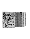
3-41 3-42 pin stop play stop play stop play stop play stop play stop play 1 1.03 2.99 0 0 1.22 1.22 3.27 3.28 0 0 0 0 2 5.11 5.08 0 0 0 0 1.18 1.26 0 0 2.59 2.55 3 0 0 8.04 8.01 0.96 0.9 1.1 1.52 0 0 0 0 4 0 0 0.12 0.06 2 2.06 0 0 0 0 2.59 2.56 5 5.11 5.07 0 0.06 0 1.51 0.66 1.07 3.28 3.29 0 0 6 0 1...
Page 47
3-43 3-44 pin stop play stop play stop play stop play stop play stop play 161 0 1.27 162 0 2.35 163 0 0 164 0 0.73 165 0 3.27 166 0 0.5 167 0 0 168 0 0.53 169 0 3.27 170 0 0.59 171 0 0 172 3.01 0.72 173 0 0.72 174 0 0 175 0 2.73 176 0 3.13 177 0 3.13 178 0 3.25 179 0 0 180 0 0 181 2.04 2.64 182 0 2....
Page 48
3-45 3-46 printed circuit diagrams 1. Main p.C.Board (top side) location guide.
Page 49
3-47 3-48 2. Main p.C.Board (bottom side) location guide.
Page 50
3-49 3-50 3 key p.C.Board location guide (solder side) (solder side) 4. Timer p.C.Board location guide.
Page 51
3-51 3-52 5. Power p.C.Board location guide (solder side).
Page 52: Contents
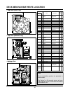
Top view..................................................4-1 top view(without tray disc) .................4-1 bottom view ...........................................4-1 1. Holder assembly clamp..................4-2 1-1. Plate clamp ......................................4-2 1-2. Magnet clamp ..........
Page 53
Starting no. 1 1,2 1,2,3 1,2,3,4 6 6 6,7 6,7,10 6,7,10,11 6,7,8,9,10, 11,12 1 1 1 1,17 1,17 1 1,15,16,17, 18,19,20 1,14 6 6,24 6,24 6,24,26 6,24,26 6,24,26,28 6,28 1,6,14,23, 24,25,26, 27,28,29, 30 1 2 3 4 5 6 7 8 9 10 11 12 13 14 15 16 17 18 19 20 21 22 23 24 25 26 27 28 29 30 31 holder assembly cl...
Page 54: Deck Mechanism Disassembly
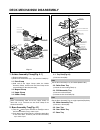
4-2 deck mechanism disassembly fig. 4-1 fig. 4-2 (a) (l1) (s1) (s1) (s1) holder clamp plate clamp plate clamp magnet clamp upper clamp holder clamp base main base assembly tray (l1) (c2) (c2) (c1) (c1) (h1) (b) base tray (s2) (s4) (s3) (s3) (c3) (s4) motor assembly tray tray disc pcb assembly tray r...
Page 55: Deck Mechanism Disassembly
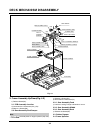
4-3 deck mechanism disassembly fig. 4-3 (s7) (s7) (s7) (s7) (s8) gear assembly rack rubber damper gear middle gear assembly feed rubber rear base pu(outsert) rubber damper pick up assembly general motor assembly spindle (c7) pick up assembly general gear assembly feed gear middle gaer assembly rack ...
Page 56: Deck Mechanism Disassembly
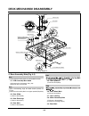
4-4 deck mechanism disassembly (s10) fig.(b) (s15) (s15) (s14) (s13) gear slider gear main gear exchange gear loading gear wheel main motor assembly main base main gear up/down fig.(c) (l4) motor assembly main pcb assembly main mode fig.(a) (s9) (s9) mode switch (c8) (s12) (s11) fig. 4-4 4. Base ass...
Page 58
Exploded views 1. Deck mechanism exploded view 011 031 001 003 004 026 025 002 414 415 415 413 413 413 414 414 416 032 034 033 035 416 416 416 416 037 030 022 023 021 020 036 a01 a02 a04 038 416 005 005 024 039 039 434 040 040 434 008b 038a 022a 008a a00 014 014 430 014 014a 014b 014 014a 014c 431 4...
Page 60
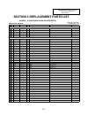
5-1 section 5 replacement parts list models : a) dvb352(dm7912nm) ha1uzz(zenith) run date:18.July.2003 .Mechanical section nsp:not service part s al loca no lg part no a description specification remarks assembly parts section a00 6721rh0342a o deck assembly,video deck/mecha dpm-4 (dvd-cd r/rw nsp a...
Page 61
5-2 s al loca no lg part no a description specification remarks screw 413 4000r-0006a o screw audio taptite 3*8(353-025b) 414 353-051e o screw special (3x12) 415 1mpc0301118 o screw machine,pan head #name? 416 4404r-0017a o mechanism audio 3*12*12(88h-0004) 430 1szzh-1003a o screw, + d2.0 6mm swrch1...
Page 62
5-3 .Electrical section s al loca no lg part no a description specification remarks bc101 636-004c o filter(circ),emc bead core bfs3550r2fd8,r t/p bd101 0dd160000da o diode s1wba60(1a 600v) shidenken c101 624-088s o capacitor,drawing mpx104k etr/europtronic bulk c102 624-088s o capacitor,drawing mpx...
Page 63
5-4 s al loca no lg part no a description specification remarks c255 0ch1104k942 o capacitor,chip[ceramic m/l hd 0.1uf 50v z y5v(f) 1508 r/tp c257 0ch1105d942 o capacitor,chip[ceramic m/l hd 1uf 10v z y5v(f) 1508 r/tp c258 0ch1105d942 o capacitor,chip[ceramic m/l hd 1uf 10v z y5v(f) 1508 r/tp c259 0...
Page 64
5-5 s al loca no lg part no a description specification remarks c425 0ch1392k562 o capacitor,fixed ceramic(temp.C 3900pf 50v k z5u(e) 1608 r/tp c426 0ce2264f638 o capacitor,electrolytic 22m sra 16v m fm5 tp(5) c502 0ch1103k562 o capacitor,fixed ceramic(temp.C 0.01uf 50v 10% x7r(x) 1608 r/t c503 0ch1...
Page 65
5-6 s al loca no lg part no a description specification remarks c566 0ch4221k412 o capacitor,chip[ceramic m/l tc 220p 50v j cog 1.6x0.8 r/tp c567 0ch4221k412 o capacitor,chip[ceramic m/l tc 220p 50v j cog 1.6x0.8 r/tp c568 0ch4221k412 o capacitor,chip[ceramic m/l tc 220p 50v j cog 1.6x0.8 r/tp c569 ...
Page 66
5-7 s al loca no lg part no a description specification remarks c901 0cn1040k948 o capacitor,fixed tubular(high d 0.1uf d 50v 80%,-20% f(y5v) ta c905 0cn6810k518 o capacitor tubula(high diele) 680p 50v k b ta26 c906 0ce1063f638 o capacitor,al.Electrolytic 10m sre/se 16v m fm5 tp(5) c907 0ce4763c638 ...
Page 67
5-8 s al loca no lg part no a description specification remarks l103 633-088g o coil,choke chock(22mh) 5mm toko tp l105 633-088g o coil,choke chock(22mh) 5mm toko tp l201 0lr0102j025 o inductor,radial lead 10uh 5% 4x5 tr5 l202 6200hjc102a o filter(circ),emc hb-1m2012-102jt ceratech tp l203 0lr0102j0...
Page 68
5-9 s al loca no lg part no a description specification remarks r124 0rd1800f608 o resistor,fixed carbon film 180 ohm 1/6 w 5% ta26 r125 0rd3901f608 o resistor,fixed carbon film 3.9k ohm 1/6 w 5% ta26 r126 0rd1001f608 o resistor,fixed carbon film 1k ohm 1/6 w 5% ta26 r127 0rn3601e408 o resistor,fixe...
Page 69
5-10 s al loca no lg part no a description specification remarks r256 0rh1002c622 o resistor,metal glazed(chip) 10k ohm 1 / 16 w 1608 5.00% d r257 0rh1002c622 o resistor,metal glazed(chip) 10k ohm 1 / 16 w 1608 5.00% d r258 0rh0000c622 o resistor,metal glazed(chip) 0 ohm 1 / 16 w 1608 5.00% d r259 0...
Page 70
5-11 s al loca no lg part no a description specification remarks r527 0rh4701c622 o resistor,metal glazed(chip) 4.7k ohm 1 / 16 w 1608 5.00% d r528 0rh1201c622 o resistor,metal glazed(chip) 1.2k ohm 1 / 16 w 1608 5.00% d r529 0rh0000c622 o resistor,metal glazed(chip) 0 ohm 1 / 16 w 1608 5.00% d r534...
Page 71
5-12 s al loca no lg part no a description specification remarks r6w4 0rh1100c622 o resistor,metal glazed(chip) 110 ohm 1 / 16 w 1608 5.00% d r6w5 0rh0222c622 o resistor,metal glazed(chip) 22 ohm 1 / 16 w 1608 5.00% d r735 0rh0000c622 o resistor,metal glazed(chip) 0 ohm 1 / 16 w 1608 5.00% d r901 0r...

