- DL manuals
- E2v
- Motherboard
- AT84AS003-EB
- User Manual
E2v AT84AS003-EB User Manual
Summary of AT84AS003-EB
Page 1
At84as003-eb evaluation board .............................................................................................. User guide.
Page 3
Table of contents at84as003-eb evaluation board user guide i 0905c–bdc–09/07 section 1 introduction ........................................................................................... 1-1 1.1 scope .................................................................................................
Page 4
Ii at84as003-eb evaluation board user guide 0905c–bdc–09/07.
Page 5: Section 1
At84as0003-eb evaluation kit user guide 1-1 0905c–bdc–09/07 section 1 introduction 1.1 scope the at84as003-eb evaluation kit is designed to facilitate the evaluation and charac- terization of the at84as003 10-bit 1.5 gsps adc with 1:2/4 dmux up to its 3 ghz full power input bandwidth and up to 1.5 g...
Page 6
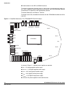
Introduction 1-2 at84as0003-eb evaluation kit user guide 0905c–bdc–09/07 potentiometers for the adc and dmux functions the board is comprised of 8 metal layers for signal traces, ground and power supply lay- ers, and 7 dielectric layers featuring low insertion loss and enhanced thermal characteris...
Page 7: Section 2
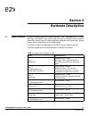
At84as003-eb evaluation kit user guide 2-1 0905c–bdc–09/07 section 2 hardware description 2.1 board structure in order to achieve optimum full-speed operation of the at84as003 10-bit 1.5 gsps adc with 1:2/4 dmux, a multi-layer board structure was retained for the evaluation board. Eight copper layer...
Page 8
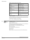
Hardware description 2-2 at84as003-eb evaluation kit user guide 0905c–bdc–09/07 the board is 1.6 mm thick. The clock, analog input, reset and digital data output signals occupy the top metal layer while the adc and dmux functions are located on both the top layer and the 15th layer. The ground plane...
Page 9
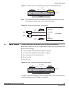
Hardware description at84as003-eb evaluation kit user guide 2-3 0905c–bdc–09/07 figure 2-1. Board layout for the differential analog, clock and dai/dain inputs note: the analog inputs are reverse terminated with 50 Ω to ground very close to the device (same line length used for both reverse terminat...
Page 10
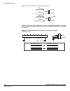
Hardware description 2-4 at84as003-eb evaluation kit user guide 0905c–bdc–09/07 figure 2-4. Differential digital outputs implementation double row 2.54 mm pitch connectors are used for the digital output data. The upper row is connected to the signal while the lower row is connected to ground, as il...
Page 11: Section 3
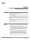
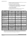
At84as003-eb evaluation kit user guide 3-1 0905c–bdc–09/07 section 3 operating characteristics 3.1 introduction this section describes a typical configuration for operating the evaluation board of the at84as003 10-bit 1.5 gsps adc with 1:2/4 dmux. The analog input signal and the sampling clock signa...
Page 12
Operating characteristics 3-2 at84as003-eb evaluation kit user guide 0905c–bdc–09/07 the digital data are differentially terminated on-board (100 Ω) however, they can be probed either in differential or in single-ended mode. 5. Connect the adc and dmux function jumpers. All instrumentation and conne...
Page 13
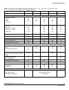
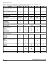
Operating characteristics at84as003-eb evaluation kit user guide 3-3 0905c–bdc–09/07 table 3-2. Operating characteristics ambient temperature (v cca = v ccd = 3.3v, v ee = -5v, v minusd = -2.2v; v plusd = 2.5v; v inn - v inn = 1 dbfs, p clk = 0 dbm differential parameter symbol min typ max unit reso...
Page 14
Operating characteristics 3-4 at84as003-eb evaluation kit user guide 0905c–bdc–09/07 clock input common voltage range (v clk or v clkn ) (dc coupled clock input) v cm -1.2 0 3.3 v clock input power level (low-phase noise sinewave input) 50 Ω single-ended or 100 Ω differential p clk -4 0 4 dbm clock ...
Page 15: Section 4
At84as003-eb evaluation kit user guide 4-1 0905c–bdc–09/07 section 4 application information 4.1 introduction for this section, refer also to the product “main features” section of the at84as003 datasheet ref 0808. 4.2 analog inputs the analog inputs can be entered in differential or in single-ended...
Page 16
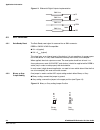
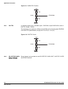
Application information 4-2 at84as003-eb evaluation kit user guide 0905c–bdc–09/07 figure 4-1. Differential digital outputs implementation 4.5 adc functions 4.5.1 data ready reset the data ready reset signal is accessed via an sma connector. Drrb is cmos/lvcmos compatible: vil = 0 (typical) vih ...
Page 17
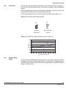
Application information at84as003-eb evaluation kit user guide 4-3 0905c–bdc–09/07 4.5.3 gain adjust the adc gain can be adjusted by the means of the ga potentiometer (varying from - 0.5v to 0.5v around 0v nominal value). A ga jumper is available to allow or disable this function. When connected to ...
Page 18
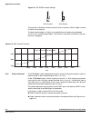
Application information 4-4 at84as003-eb evaluation kit user guide 0905c–bdc–09/07 figure 4-5. Dc sdaen jumper settings the variation of the delay around its nominal value as function of sda voltage is shown in figure 4-6 on page 4-4. The typical tuning range is ±120 ps for an applied control voltag...
Page 19
Application information at84as003-eb evaluation kit user guide 4-5 0905c–bdc–09/07 figure 4-7. Pattern generator enable jumper position 4.6 dmux function 4.6.1 asyncrst the asynchronous reset is mandatory to start the device properly. It mustbe applied after power up of the device. A push button is ...
Page 20
Application information 4-6 at84as003-eb evaluation kit user guide 0905c–bdc–09/07 figure 4-9. Clkdactrl function 4.6.3 dactrl a standalone delay cell is available (input = dai/dain, output dao/daon, control = dactrl, enable = daen). This cell allows you to delay by ±250 ps (around 250 ps) the incom...
Page 21
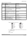
Application information at84as003-eb evaluation kit user guide 4-7 0905c–bdc–09/07 figure 4-11. Smux functions and description figure 4-12. Dmux functions jumper positions note: the bist is made of a 10-bit sequence available on all 4 ports of the device (set the at84as003 in 1:4 mode). The sequence...
Page 22
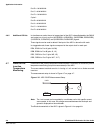
Application information 4-8 at84as003-eb evaluation kit user guide 0905c–bdc–09/07 port b = 1010101010 port c = 0101010101 port d = 1010101010 cycle 1: port b = 0101010101 port a = 0101010101 port c = 1010101010 port d = 0101010101 4.6.5 additional or bits in simultaneous mode, the out of range sign...
Page 23
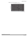
Application information at84as003-eb evaluation kit user guide 4-9 0905c–bdc–09/07 figure 4-14. Adc diode characteristics (1 = 1 ma) junction temperature versus diode voltage for i =1 ma 790 800 810 820 830 840 850 860 870 880 890 900 910 920 930 940 950 -10 0 10 20 30 40 50 60 70 80 90 100 110 junc...
Page 24
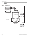
Application information 4-10 at84as003-eb evaluation kit user guide 0905c–bdc–09/07 4.8 test bench description figure 4-15. Test bench schematics bpf demux power supplies gw ppt 0 o c balun macom - h9 acquisition board power supplies gw ppt hp16500c analysis logic a b c d gpib bus fs = adc sampling ...
Page 25: Section 5
At84as003-eb evaluation kit user guide 5-1 0905c–bdc–09/07 section 5 package information 5.1 thermal characteristics an external heat sink must be placed on top of package. It is advised to use an external heat sink with intrinsic thermal resistance better than 4 °c/watt when using air at room tempe...
Page 26
Package information 5-2 at84as003-eb evaluation kit user guide 0905c–bdc–09/07.
Page 27: Section 6
At84as003-eb evaluation kit user guide 6-1 0905c–bdc–09/07 section 6 ordering information table 6-1. Part number package temperature range screening comments at84xas003tp ebga 317 ambient prototype prototype version please contact your local sales office at84as003ctp ebga 317 commercial “c” 0°c c ; ...
Page 28
Ordering information 6-2 at84as003-eb evaluation kit user guide 0905c–bdc–09/07.
Page 29: Section 7
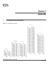
At84as003-eb evaluation kit user guide 7-1 0905c–bdc–09/07 section 7 appendix 7.1 at84as003-eb electrical schematics figure 7-1. Power supplies decoupling decoupling decoupling decoupling decoupling decoupling decoupling.
Page 30
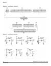
Appendix 7-2 at84as003-eb evaluation kit user guide 0905c–bdc–09/07 figure 7-2. Power supplies connection figure 7-3. Power supplies bypassing.
Page 31
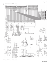
Appendix at84as003-eb evaluation kit user guide 7-3 0905c–bdc–09/07 figure 7-4. At84as003-eb electrical schematic.
Page 32
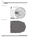
Appendix 7-4 at84as003-eb evaluation kit user guide 0905c–bdc–09/07 7.2 at84as003-eb board layers figure 7-5. Top layer figure 7-6. Bottom layer.
Page 33
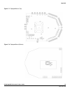
Appendix at84as003-eb evaluation kit user guide 7-5 0905c–bdc–09/07 figure 7-7. Equipped board (top) figure 7-8. Equipped board (bottom).
Page 34
Appendix 7-6 at84as003-eb evaluation kit user guide 0905c–bdc–09/07.
Page 35
Whilst e2v has taken care to ensure the accuracy of the information contained herein it accepts no responsibility for the consequences of any use thereof and also reserves the right to change the specification of goods without notice. E2v accepts no liability beyond that set out in its stan- dard co...

