- DL manuals
- FastVision
- Digital Camera
- FastCamera13
- User Manual
FastVision FastCamera13 User Manual
Summary of FastCamera13
Page 1
Fastcamera series fastcamera13 user’s manual fvm-50013.
Page 2
2 copyright notice copyright © 2004 by fastvision, llc. All rights reserved. This document, in whole or in part, may not be copied, photocopied, reproduced, translated, or reduced to any other electronic medium or machine-readable form without the express written consent of fastvision, llc. Fastvisi...
Page 3
3 table of contents 1. Introduction _________________________________________________ 1-6 2. Features and specifications _______________________________________ 2-6 2.1. Camera specifications ____________________________________________ 2-7 2.2. Image sensor specifications: _________________________...
Page 4
4 13.9. Power-on initialization _____________________________________________ 13-17 14. Flash memory_________________________________________________ 14-18 15. Camera state storage __________________________________________ 15-19 16. Serial control interface _________________________________________...
Page 5
5 24. Troubleshooting __________________________________________ 24-50 25. Fastvision technical support________________________________ 25-50 25.1. Contacting technical support_______________________________________ 25-50 25.2. Returning products for repair or replacements _______________________ 25...
Page 6
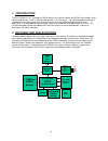
6 1. Introduction the fastcamera13 is a 1.3 megapixel cmos camera with internal memory and fpga’s that enable it to do real-time processing. Thus it is what one would term a “smart” camera. The standard programming that is supplied with the base camera forms the basis of the most used and demanded f...
Page 7
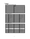
7 2.1. Camera specifications • the fastcamera13 uses a 1280h x 1024v (1.3 megapixel) cmos digital image sensor capable of 500 frames/second operation at full resolution • 1280h x 1024v image resolution • 12-micron-square active-pixel photodiodes • 500+ frames per second, progressive-scan • at full r...
Page 8
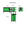
8 12 .7 m m 0 ref 39.5m m 74.0m m 0 r e f 7m m 1 32m m 12.7mm 7m m 0 ref 0 r e f 39. 5m m 79. 0m m j3 j2 p2 fastcam era13 front view fastcam era13 case and m o unting dim ensio ns fastcam era13 side view fastcam era13 back panel fastcam era13 bottom view.
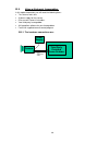
Page 9
9 2.4. Connectors 2.4.1. Power connector hr10a-10r-12pb pin function 1 ground 2 +5 volts 3 ground 4 reserved for application dependent i/o 5 ground 6 +5 volts 7 reserved for application dependent i/o 8 ground 9 +5 volts 10 reserved for application dependent i/o 11 +5 volts 12 reserved for applicatio...
Page 10
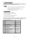
10 3. Power requirements power requirements are a strong function of the specific application; the camera is 15 watts worst case, 5 to 10 watts typical. Low noise +5 volt input recommended. Internally the camera has high frequency switching supplies that convert the 5 volt input to 3.3, 2.5 and 1.8 ...
Page 11
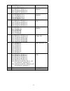
11 cl1_c[7:0] pixels 4*n+2 cl2_a[7:0] pixels 4*n+3 8 cl1_b[1:0],cl1_a[7:0] 4*n+0 cl1_b[5:4],cl1_c[7:0] 4*n+1 cl2_c[1:0],cl2_b[7:0] 4*n+2 cl2_c[4:5],cl2_a[7:0] 4*n+3 four taps 10 bits (medium) 9 cl1_a[7:0] pixels 5*n+0 cl1_b[7:0] pixels 5*n+1 cl1_c[7:0] pixels 5*n+2 cl2_a[7:0] pixels 5*n+3 cl2_b[7:0]...
Page 12
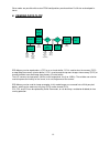
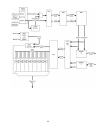
12 other modes are possible with custom fpga configurations purchased from fastvision or developed in- house. 6. Camera data flow sensor 128-1000m b ddr memory sram lut by pixel gain & offset data format funnel camera links mem lut exposure control cc1 cc2 cc3 read memory serial settings ddr tables ...
Page 13
13 7. The standard camera functionality the ‘standard’ camera is a set of fpgas designed to support most of the typical uses of the camera. It is a good starting point for modifications. This design is copyrighted ip from fastvision and forms the reference design, which is available from fastvision ...
Page 14
14 9.2. Circular buffer memory mode in this mode the memory is used as a circular buffer. Each time an image is presented to the memory it is stored over-writing the oldest image in the buffer. When cc2 goes active (or via a serial command), the filling operation stops, after a selected number of fr...
Page 15
15 13.1. Line timing sensor line and frame rates are controlled by the camera state settings. The minimum line period depends on the sensor type and the roi width. When the line period setting exceeds the minimum period, extra clocks are inserted between lines. The line valid period only depends on ...
Page 16
16 there are four basic trigger modes: • free-running mode ignores trigger inputs and reads out the sensor continuously at a programmed frame rate with programmed exposure timing. • multi-frame edge-triggered mode activates a programmed number of exposures after a programmed delay at a programmed fr...
Page 17
17 there are four trigger sources - camera link cc1, ttl trigger input, serial, and usb (via i2c). • the cc1 and ttl sources can be enabled or disabled. They can also be active high (positive-going edge for edge-triggering or high level for external exposure) or active low (negative-going edge for e...
Page 18
18 the control fpga has a small embedded micro that runs through an initialization sequence at power-on. This same micro also implements the host, usb, and data fpga communication protocols and deals with flash memory and dac’s. 1. Immediately after power-on, the voltage reference dac’s are programm...
Page 19
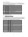
19 table 2 - flash memory layout table 3 shows the layout of the first page in flash memory. This contains enough descriptors for the camera control gui to determine the camera type and its options. This data should only be programmed by fast-vision. The camera gui software must enforce this, as the...
Page 20
20 40 2 roi start line 42 2 roi end line 44 2 line period in pixel clocks 46 4 exposure time in pixel clocks 50 4 frame period in pixel clocks 54 4 exposure delay in pixel clocks 58 2 serial link bit period in pixel clocks 60 1 camera link readout mode 61 1 camera link clock frequency 62 1 binning 6...
Page 21
21 16.1. Encoding commands and response use the 7-bit ascii code zero-extended to 8 bits. This is sometimes refered to as 8 bits, no parity or 7-bits space parity. For characters that require escape codes as listed below, the 8 th bit is significant in the decoding, so only the normal character enco...
Page 22
22 all commands end in a non-escaped carriage-return, hex 0d. When commands take arguments in hex, data must consist of pairs of hex characters representing full bytes. Within each byte the most significant nibble is sent first, but for multi-byte values the least significant byte is normally sent f...
Page 23
23 this command takes no arguments. The camera responds with “h” followed by eight hex digits and a carriage-return. The eight hex digits indicate the value of a free-running 32-bit frame counter. This counter indicates all frames read from the sensor since power on, not necessarily the number of fr...
Page 24
24 0x85 main memory page program through buffer 2 the following non-write commands are also implemented with write flash: 0x53 main memory page to buffer 1 transfer 0x55 main memory page to buffer 2 transfer 0x60 main memory page to buffer 1 compare 0x61 main memory page to buffer 2 compare 0x58 aut...
Page 25
25 this is the only control fpga response that uses binary encoded arguments (with escape codes for and \). The camera responds with “m” followed by escaped binary data from the flash and finally a non-escaped carriage-return. Internally the control fpga waits for the flash to become non-busy then s...
Page 26
26 serial commands commands from the host are buffered and passed to the data fpga on the fpga_ctl3 wire. The data fpga therefore receives all commands from the host and can act on them accordingly. This allows extensions to be made to the command set for data fpga use. To reduce logic in the data f...
Page 27
27 the picoblaze data address space is only 256 bytes. If you look at the processor documents from xilinx you’ll find this called i/o rather than data. In our case the data space connects to 1k bytes of internal block ram using three additional banking bits implemented as register. Access to the ent...
Page 28
28 4 serial trigger. Must be toggled in software to trigger the sensor control logic in response to a serial trigger command. 3 reserved. 2 calibrate sensor. This is a pulsed signal that schedules a calibration when this bit is written to 1. Writing this bit to zero has no effect. Actual calibration...
Page 29
29 0xff fpga configuration. Bit 6 is reserved. Other bits are: 7 read only “fget8” status. This is high when the sequencer is still running from a prior operation. 5 fpga loaded on write, fpga done on read. Writing this bit high indicates that the program has finished loading the data fpga and enabl...
Page 30
30 0x2c line period, low 8 bits. 0x2d line period, high 8 bits. This is the line readout time in pixel clocks - 1. I.E. The actual period is one clock more than this number. 0x2e exposure period, bits 0x2f exposure period, bits 0x30 exposure period, bits 0x31 exposure period, bits this is the desire...
Page 31
31 0 enable camera link cc2. Set this bit to 1 to enable cc2 readout image. When enabled, the active edge of cc2 causes the current memory image to be read out. 19. Data fpga this specification contains an overview of the functionality and design details for the data fpga within the fastcamera 13/40...
Page 32
32.
Page 33
33 19.2. Video data path overview the datafpga accepts video data from the sensor and formats it for transmission over the camera link outputs or usb interface. The controlfpga controls the sensor data output and sends lval (line valid) and fval (frame valid) signals to the datafpga. The data from t...
Page 34
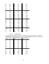
34 12 2 vbias1: 30 00 14 2 vref3: 32 e8 16 2 vbias2: 40 00 18 2 vref4: 41 36 20 2 vbias3: 50 00 22 2 vln1: 54 d9 24 2 vbias4: 60 00 26 2 vlp: 64 d9 28 2 vunused1: 70 00 30 2 vclamp3: 70 00 32 2 vunused2: 80 00 34 2 vrstpix: 8d 17 36 2 roi start pixel 38 2 roi end pixel 40 2 roi start line 42 2 roi e...
Page 35
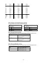
35 0x00 cl1_a[7:0] single tap 8 bits (basic) 0x01 cl1_b[1:0],cl1_a[7:0] single tap 10 bits (basic) (default mode) 0x02 cl1_b[3:0],cl1_a[7:0] single tap 12-bits (basic) 0x03 cl1_b[7:0],cl1_a[7:0] single tap 16-bits (basic) 0x04 cl1_a[7:0] even pixels (0,2,...) cl1_b[7:0] odd pixels (1,3,...) two taps...
Page 36
36 a2 tx2 c8 tx2 f5 tx2 a3 tx3 c9 tx3 f6 tx3 a4 tx4 d0 tx4 f7 tx4 a5 tx5 d1 tx5 f8 tx5 a6 tx6 d2 tx6 f9 tx6 a7 tx7 d3 tx7 g0 tx7 a8 tx8 d4 tx8 g1 tx8 a9 tx9 d5 tx9 g2 tx9 b0 tx10 d6 tx10 g3 tx10 b1 tx11 d7 tx11 g4 tx11 b2 tx12 d8 tx12 g5 tx12 b3 tx13 d9 tx13 g6 tx13 b4 tx14 e0 tx14 g7 tx14 b5 tx15 e...
Page 37
37 b6 tx14 f0 tx14 j3 tx14 b7 tx15 f1 tx15 j4 tx15 c0 tx16 f2 tx16 j5 tx16 c1 tx17 f3 tx17 j6 tx17 c2 tx18 f4 tx18 j7 tx18 c3 tx19 f5 tx19 k0 tx19 c4 tx20 f6 tx20 k1 tx20 c5 tx21 f7 tx21 k2 tx21 c6 tx22 g0 tx22 k3 tx22 c7 tx23 g1 tx23 k4 tx23 lval tx24 g2 tx24 k5 tx24 fval tx25 g3 tx25 k6 tx25 d0 tx...
Page 38
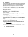
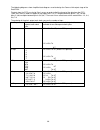
38 20. Frame rates. The actual frame rate of the camera is determined by settings within the controlfpga and the datefpga. The controlfpga settings determine the data rate from the sensor by adjusting the roi (region of interest), exposure rate and exposure delay. The datafpga settings determine the...
Page 39
39 the following diagrams show simplified state diagrams used to design the camera link output stage of the datafpga. The data from the fifos are fed to 5-to-1 muxes on order to limit the fanout of the data from the fifo. There are 8 muxs in order to support 8 tap mode. Muxs 1,3,5,7 multiplex betwee...
Page 40
40 the following notes apply for these timing diagrams • clk0 is the camera link output clock • empty is the signal from the fifo that starts the state machine operation in these simplified state diagrams. The actual verilog code used a combination of empty and other conditions to insure that the fi...
Page 41
41 20.4. 2 tap mode when the fifo deasserts empty the state machine starts with a pre-read of the whole fifo during which pixels 1-ten are read. The state machine then continues in a 5 cycle loop until the end of the line is detected (ff_lval deasserted). The output from muxs 1, 2 drive the two taps...
Page 42
42 20.5. 4 tap mode when the fifo deasserts empty the state machine starts with a pre-read of the whole fifo during which pixels 1-ten are read. The state machine then continues in a 5 cycle loop until the end of the line is detected (ff_lval deasserted). The output from muxs 1,2,3,4 drives the four...
Page 43
43 20.6. 8 tap mode when the fifo deasserts empty the state machine starts with a pre-read of the whole fifo during which pixels 1-ten are read. The state machine then continues in a 5 cycle loop until the end of the line is detected (ff_lval deasserted). The output from muxs 1, 2,3,4,5,6,7,8 drive ...
Page 44
44 20.7. Sensor interface the fpga interface to the sensor consists of the following signals: • mv_hsck4,2,1,0 • mv_hsck0, • mv_hsck1, • mv_hsck2, • mv_hsck4, • mv_sel0, • mv_sel1, • mv_sel2, • mv_sel4, • mv_hsd, • mv_data.
Page 45
45 21. Usb camera option all cameras are shipped with a usb interface for control and readout of the camera. This allows the camera to be operated with or without a framegrabber, and helps diagnose system problems when a framegrabber is being used. A camera control program comes with the camera, whi...
Page 46
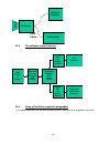
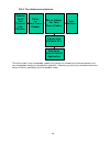
46 cam era pow er supply le ns com puter usb cable 23.3. The software connections are: usb device in camera your software library, dll or activex control operating system provided usb drivers fastvision provided usb device driver fastvision fastviewer software library, dll or activex control 23.4. U...
Page 47
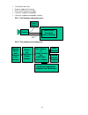
47 the camera and a lens a power supply for the camera one or more camera link cables fastvision supplied framegrabber fastvision supplied framegrabber software. 23.4.1. The hardware connections are: camera le ns your computer power supply fastvision provided frame grabber 1 or 2 camera link cables ...
Page 48
48 23.5. Using a third-party framegrabber in this mode of operation you will need the following items: the camera and a lens a power supply for the camera. One or more camera link cables. Your third-party framegrabber. Aia compliant software for your framegrabber. Fastvision supplied camera control ...
Page 49
49 23.5.2. The software connections are: camera serial and channel link devices driver for your frame grabber dll or library for your frame grabber your software camera link standard dll fastvision camera control application this will only work if your framegrabber supports the camera link standard ...
Page 50
50 24. Troubleshooting there are several things you can try before you call fastvision technical support for help. _____ make sure the computer is plugged in. Make sure the power source is on. _____ go back over the hardware installation to make sure that the system is properly installed. _____ go b...
Page 51
51 when calling for an rma number, please have the following information ready: _____ serial numbers and descriptions of product(s) being shipped back _____ a listing including revision numbers for all software, libraries, applications, daughter cards, etc. _____ a clear and detailed description of ...
Page 52
52 remember to include the name and telephone number of the person we should contact if we have questions. Fastvision, llc. 131 daniel webster highway #529 nashua, nh 03060 usa telephone: 603-891-4317 fax: 603-891-1881 web site: http://www.Fast-vision.Com/ electronic mail: sales@fast-vision.Com supp...


