- DL manuals
- Icom
- Transceiver
- IC-F14
- Service Manual
Icom IC-F14 Service Manual
Summary of IC-F14
Page 1
Service manual vhf transceivers ic-f14 ic-f14s ic-f15 ic-f15s.
Page 2
Introduction danger ordering parts repair notes this service manual describes the latest service information for the ic-f14/ic-f14s/ic-f15/ic-f15s vhf transceiv- er at the time of publication. Never connect the transceiver to an ac outlet or to a dc power supply that uses more than 8 v. Such a conne...
Page 3
Table of contents section 1 specifications section 2 inside views section 3 disassembly instructions section 4 circuit descripiton 4-1 receiver circuits . . . . . . . . . . . . . . . . . . . . . . . . . . . . . . . . . . . . . . . . . . . . . . . . . . . . . 4-1 4-2 transmitter circuits . . . . . . ...
Page 4: Section 1
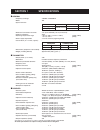
1 - 1 section 1 specifications general • frequency coverage : 136.000–174.000 mhz • mode : fm • type of emission : version wide middle narrow [usa], [gen] 16k0f3e (25.0 khz) n/a 11k0f3e (12.5 khz) [eur] 14k0f3e (20.0 khz) 8k0f3e (12.5 khz) • number of conventional channels : 2 ch (ic-f14s/f15s), 16 ...
Page 5: Section 2
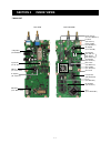
Section 2 inside views • main unit 2 - 1 +5 regulator (ic9: njm2870) af amplifier (ic12: ta7368f) d/a converter (ic8: m62363fp) r5 regulator (q22: 2sa1577) cpu (ic13: hd6433687) s5 regulator q23: 2sb1132 q24: xp6501 q25: unr9113j crystal filter (fi1: fl-335) fm if ic (ic1: ta31136fn) if amplifier (q...
Page 6: Section 3
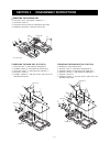
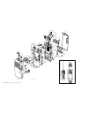
Section 3 disassembly instructions 3 - 1 chassis unit d a * b c e *: ic-f14/f15 only main unit i k k l k f g chassis unit l h h j shield cover • removing the chassis unit 1 unscrew 1 nut a, and remove 2 knobs b, c. 2 unscrew 2 screws d. 3 take off the chassis unit in the direction of the arrow. 4 un...
Page 7: Section 4
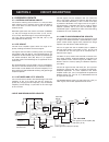
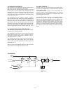
4 - 1 section 4 circuit description 4-1 receiver circuits 4-1-1 antenna switching circuit the antenna switching circuit functions as a low-pass filter while receiving and a resonator circuit while transmitting. This circuit does not allow transmit signals to enter the receiver circuits. Received sig...
Page 8
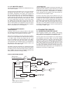
4 - 2 4-1-5 af amplifier circuit the af amplifier circuit amplifies the demodulated af sig- nals to drive a speaker. The af signals from the fm if ic (ic1, pin 9) pass through the high-pass filter (ic6, pins 3 and 1) to suppress unwant- ed harmonic components. The signals pass through the rx mute sw...
Page 9
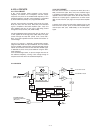
4-2-2 modulation circuit the modulation circuit modulates the vco oscillating signal (rf signal) using the microphone audio signals. The af signals from the d/a converter (ic8, pin 3) change the reactance of varactor diode (d18) to modulate the oscil- lated signal at the tx vco circuit (q13, d16, d1...
Page 10
4-3 pll circuits 4-3-1 pll circuit a pll circuit provides stable oscillation of the transmit frequency and receive 1st lo frequency. The pll output compares the phase of the divided vco frequency to the reference frequency. The pll output frequency is controlled by the divided ratio (n-data) of a pr...
Page 11
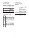
4 - 5 line vcc +5v s5v r5v t5v description the voltage from the connected battery pack. Common 5 v converted from the vcc line at the +5 regulator circuit (ic9). The output voltage is supplied to the d/a converter (ic8), analog sw (ic10) and so on. Common 5 v converted from the vcc line at the s5 re...
Page 12
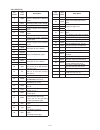
6 pin number port name description 1 temp input port for the transceiver’s internal temperature detecting signal. 2 batv input port for the detect signal for connecting battery pack’s voltage. 7 res input port for power reset signal. 13 senc0 output single tone encoder signal. 14 senc1 16 duse o u t...
Page 13
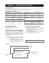
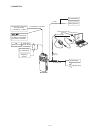
5 - 1 section 5 adjustment procedures 5-1 preparation when adjusting ic-f14/s, the optional cs-f14 adj adjustment software (rev. 1.0 or later), jig cable (see the illust below) and opc-478 cloning cable (rs-232 type) or opc-478u (usb type) are required. Required test equipment system requirements • ...
Page 14
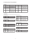
2 5-2 configulation list for adjustments channel frequency setting condition channel frequency setting condition 1 174.000 mhz set tx power to high. 6 155.000 mhz set tx power to low1. Set if bandwidth to narrow. 2 174.000 mhz set tx power to low2. 7 155.000 mhz set tx power to low1. Set if bandwidt...
Page 15
(connection 5 - 3 fm deviation meter sinad meter speaker (8 Ω) audio generator ac millivoltmeter to the antenna connector attenuator 20 db / 30 db rf power meter 0.1–10 w/50 Ω frequency counter standard signal generator 0.1 µv to 32 mv (–127 dbm to –17 dbm) do not transmit while an ssg is connected ...
Page 16
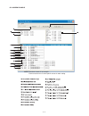
5 - 4 (pc screen example note: the above screen is an example. Each transceiver has its own specific values for each setting..
Page 17
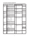
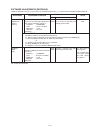
5 - 5 5-3 software adjustments (transmitting) select an operation using [ ↑] / [↓] keys, then set specified value using [←] / [→] keys on the connected computer keyboard. 1 2 3 4 1 1 2 3 1 2 3 1 2 3 1 • operating ch : ch3 (*ch1) • receiving • operating ch : ch3 (*ch1) • connect an rf power meter or ...
Page 18
5 - 6 side pannel side panel minimum distortion level set “sql level” to close squelch. Then set “sql level” at the point where the audio signals just appears. Software adjustments (receiving) • select an operation using [ ↑] / [↓] keys, then set specified value using [←] / [→] keys on the connected...
Page 19: Section 6
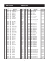
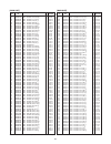
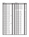
[main unit] [main unit] ic1 1110003200 s.Ic ta31136fn (el) b 51.8/19 ic2 1110002750 s.Ic ta75s01f (te85r) t 68.9/21 ic4 1140005990 s.Ic mb15a02pfv1-g-bnd-er t 38.3/35.7 ic5 1110005340 s.Ic njm12902v-te1 t 29.7/11.6 ic6 1110005320 s.Ic njm13403v-te1 t 16/34.6 ic7 1110005340 s.Ic njm12902v-te1 t 29.9/...
Page 20
6-2 [main unit] [main unit] r14 7030005050 s.Res erj2gej 103 x (10 k \ ) t 80.6/35.7 r15 7030005310 s.Res erj2gej 124 x (120 k \ ) b 79.8/39 r16 7030008280 s.Res erj2gej 271 x (270 \ ) b 74.8/39.9 r17 7030004970 s.Res erj2gej 470 x (47 \ ) b 74.8/33.9 r18 7030005530 s.Res erj2gej 100 x (10 \ ) t 79....
Page 21
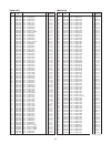
6-3 [main unit] [main unit] r183 7030006020 s.Res rr0510p-682-d (6.8 k \ ) b 17.6/39.5 r184 7030008250 s.Res rr0510p-562-d (5.6 k \ ) b 17.6/41.2 r185 7030005100 s.Res erj2gej 154 x (150 k \ ) b 18.6/41.2 r186 7030005310 s.Res erj2gej 124 x (120 k \ ) t 19.4/29.8 r187 7030005120 s.Res erj2gej 102 x ...
Page 22
4 [main unit] [main unit] s.=surface mount ref order description m. H/v no. No. Location ref order description m. H/v no. No. Location m.=mounted side (t: mounted on the top side, b: mounted on the bottom side) c65 4030017460 s.Cer ecj0eb1e102k b 46.5/18.6 c66 4030017460 s.Cer ecj0eb1e102k b 47.5/13...
Page 23
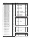
6-5 [main unit] ref order description m. H/v no. No. Location m.=mounted side (t: mounted on the top side, b: mounted on the bottom side) c258 4030017790 s.Cer ecj0eb1e682k t 30.6/39.1 c259 4030018860 s.Cer ecj0eb0j105k t 26.9/41.1 c260 4030017730 s.Cer ecj0eb1e471k t 28.6/39.1 c261 4030016930 s.Cer...
Page 24: Section 7
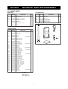
Section 7 mechanical parts and disassembly 7 - 1 s1 2260002870 as-243-a13 [f14s], [f15s] 1 sp1 2510001060 k036na500-47 1 w1 8900009640 opc-963 1 w2 8900009640 opc-963 [f14s], [f15s] 1 j1 6910015910 antenna connector 1 j2 6910015860 imsa-6277s-02a-g 1 mp1 8010019690 2775 chassis 1 mp2 8210020920 2775...
Page 25
7 - 2 unit abbreviation (c): chassis parts, (m): main unit a a mp25(c) *mp11(c) mp10(c) mp9(c) mp33(c) mp20(c) sp1(c) main unit mp28(c) mp28(c) mp4(m) mp28(c) mp28(c) mp21(c) mp22(c) mp34(c) mp28(c) mp16(c) mp28(c) s4(m) r226(m) connect unit mp29(c) mp30(c) ant unit mp1(c) j1(c) mp36(c) mp35(c) mp17...
Page 26
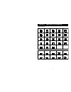
Section 8 semi-conductor information 8 - 1 • diodes • transistor and fet’s 2sa1577 q (symbol: hp) 2sa2048tl r (symbol: ul) 2sc4081 r (symbol: br) 2sb1132 r (symbol: barb) b e c b e c 2sa1576 r (symbol: fr) b e c b c e e c b 2sc4116 bl (symbol: ll) e c b 2sc4226 r25 (symbol: br) e c b 2sc5107 (symbol...
Page 27
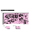
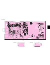
Sp1 c348 c266 r256 r200 r201 c349 c292 c294 r262 r198 r197 r263 c293 r196 c310 c291 c253 r151 r149 r145 c251 r147 r146 r148 c252 c290 r150 c254 c241 r141 c243 r142 c242 r36 r143 c279 c166 l33 r140 c72 r229 c323 c318 r228 r240 c314 r230 r54 c322 r227 c315 r232 r233 c316 r231 c319 c320 c324 r133 c88 r...
Page 28
• bottom view c16 c14 c6 c176 l3 c5 c175 c8 l6 c2 l7 c18 c19 c17 c25 l31 c22 c29 c28 l9 l8 d8 d4 c26 c20 d5 mp1 l1 s2 s1 r20 c40 c48 l12 r29 c50 r31 c53 c54 c55 r32 fi1 q16 c56 c91 c160 c58 r221 c265 q28 c306 r223 c307 c75 c264 c237 c309 1 c15 c10 c9 r224 c312 c227 c326 c228 l5 d1 c12 c230 c229 c172...
Page 29
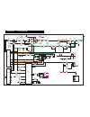
Section 10 block diagram 10 - 1 notes : contorol line common line tx line rx line data lime voltage line bal ic7: njm12902 x2: cr-783 15.3 mhz q19: 2sc4116 ref x3 bpf pll ic ic4: mb15a02 tcxo lvin s5v loop fil ripple fil q20: 2sk3019 buff charge pump buff 45.9 mhz sqin det mod lva, t1, t2 d/a fm if ...
Page 30
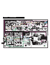
Section 11 voltage diagram 11 - 1 11-1 main unit voltage line notes : common line tx line rx line vcc c211 1 r102 270 k r103 1 m c159 0.001 ep3 c158 0.1 cp1 c143 0.001 c141 0.001 r100 10 k r101 1 k c135 0.001 r92 100 k c137 0.01 c190 5 p d20 hvc376b c203 0.001 d22 hvc375b c1 15 33 p c134 18 p c1 14 ...
Page 31
Asia icom inc. 6f no.68, sec. 1 cheng-teh road, taipei, taiwan, r.O.C. Phone : +886 (02) 2559 1899 fax : +886 (02) 2559 1874 url : http://www.Asia-icom.Com e-mail : sales@asia-icom.Com zac de la plaine, 1, rue brindejonc des moulinais bp 5804, 31505 toulouse cedex, france phone : +33 (5) 61 36 03 03...
Page 32
1-1-32, kamiminami, hirano-ku, osaka, 547-0003, japan s-14111iz-c1 © 2004 icom inc..

