- DL manuals
- Icom
- Transceiver
- IC-F24
- Service Manual
Icom IC-F24 Service Manual
Summary of IC-F24
Page 1
Service manual uhf transceivers.
Page 2
Introduction this ser vice manual descr ibes the latest ser vice information for the ic-f24/ic-f24s/ic-f25/ic-f25s uhf transceiver at the time of publication. Danger never connect the transceiver to an ac outlet or to a dc power supply that uses more than 8 v. Such a connection could cause a fire or...
Page 3
Table of contents section 1 specifications section 2 inside views section 3 disassembly instructions section 4 circuit descripiton 4-1 receiver circuits . . . . . . . . . . . . . . . . . . . . . . . . . . . . . . . . . . . . . . . . . . . . . . . . . . . . . . . 4-1 4-2 transmitter circuits . . . . ...
Page 4: Section 1
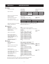
1 - 1 section 1 specifications general • frequency coverage : 400–470 mhz [usa–02], [gen–02], [eur] 450–512 mhz [usa–03] 450–520 mhz [gen–03] • type of emission : • number of conventional channels : 2 ch (ic-f24s/f25s), 16 ch (ic-f24/f25) • antenna impedance : 50 Ω (nominal) • operating temperature ...
Page 5
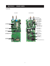
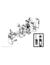
Section 2 inside views • main unit 2 - 1 +5 regulator (ic9: njm2870) af amplifier (ic12: ta7368f) d/a converter (ic8: m62363fp) r5 regulator (q22: 2sa1577) cpu (ic13: hd6433687a91fp) s5 regulator q23: 2sb1132 q24: xp6501 q25: unr9113j crystal filter (fi1: fl-335) fm if ic (ic1: ta31136fn) if amplifi...
Page 6
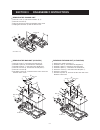
Section 3 disassembly instructions 3 - 1 chassis unit d a *b c e *: ic-f24/f25 only shield cover earth plate main unit k m m n m f g chassis unit n l i h • removing the chassis unit 1 unscrew 1 nut a, and remove 2 knobs *b, c. 2 unscrew 2 screws d. 3 take off the chassis unit in the direction of the...
Page 7: Section 4
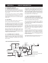
4 - 1 section 4 circuit description 4-1 receiver circuits 4-1-1 antenna switching circuit the antenna switching circuit functions as a low-pass filter while receiving and a resonator circuit while transmitting. This circuit does not allow transmit signals to enter the receiver circuits. Received sig...
Page 8
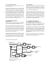
4 - 2 4-1-5 af amplifier circuit the af amplifier circuit amplifies the demodulated af sig- nals to drive a speaker. The af signals from the fm if ic (ic1, pin 9) pass through the high-pass filter (ic6, pins 3 and 1) to suppress unwant- ed harmonic components. The signals pass through the rx mute sw...
Page 9
4-2-2 modulation circuits the modulation circuit modulates the vco oscillating signal (rf signal) using the audio signals from the microphone. The af signals from the d/a converter (ic8, pin 3) change the reactance of varactor diode (d18) to modulate the oscil- lated signal at the tx vco circuit (q1...
Page 10
4-3 pll circuits 4-3-1 pll circuit a pll circuit provides stable oscillation for the transmit fre- quency and the receive 1st lo frequency. The pll output compares the phase of the divided vco frequency to the reference frequency. The pll output frequency is controlled by the divided ratio (n-data) ...
Page 11
4 - 5 line vcc +5v s5v r5v t5v description the voltage from the connected battery pack. Common 5 v converted from the vcc line at the +5 regulator circuit (ic9). The output voltage is supplied to the d/a converter (ic8), analog sw (ic10), etc. Common 5 v converted from the vcc line at the s5 regulat...
Page 12
6 pin number port name description 1 temp input port for the transceiver’s internal temperature detecting signal. 2 batv input port for the detect signal for connecting battery pack’s voltage. 7 res input port for power reset signal. 13 senc0 output single tone encoder signal. 14 senc1 16 duse o u t...
Page 13
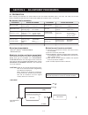
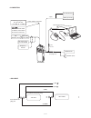
5 - 1 section 5 adjustment procedures 5-1 preparation when adjusting ic-f24/f25/s, the optional cs-f14 adj adjustment software (rev. 1.0 or later), jig cable (see the illust below) and opc-478 (rs-232 type) or opc-478u (usb type) cloning cable are required. Required test equipments system requiremen...
Page 14
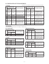
2 5-2 configulation list for adjustments - ic-f24s/f25s - • re-clone these settings every time each category is adjusted. (1−8). Ch. Frequency (mhz) setting condition [us2], [eu2], [ge2] [us3], [ge3] 1 400.000 450.000 set tx power to high. 2 400.000 450.000 set tx power to low2. 3 400.000 450.000 se...
Page 15
(connection 5 - 3 opc-478/u jig cable to ic-f24/f25/s [sp] jack 3-conductor 3.5(d) mm plug ( sp + ) (clone) (gnd) (sp − ) (jig cable fm deviation meter sinad meter speaker (8 Ω) audio generator ac millivoltmeter to the antenna connector attenuator 20 db / 30 db rf power meter 0.1–10 w/50 Ω frequency...
Page 16
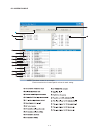
5 - 4 (pc screen example note: the above screen is an example. Each transceiver has its own specific values for each setting..
Page 17
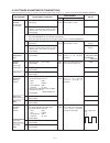
5 - 5 5-3 software adjustments (transmitting) select the operation using [ ↑] / [↓] keys, then set specified value using [←] / [→] keys on the connected computer keyboard. Set to square wave form *for f24s/f25s adjustment. Adjustment adjustment condition measurement value unit location pll lock volt...
Page 18
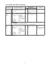
5 - 6 5-3 software adjustments (receiving) • select an operation using [ ↑] / [↓] keys, then set specified value using [←] / [→] keys on the connected computer keyboard. *for f24s/f25s adjustment. Adjustment adjustment condition measurement value unit location ctcss/dtcs deviation [ctcs/dtcs] 1 • op...
Page 19: Section 6
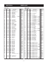
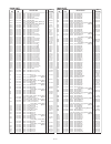
6 - 1 section 6 parts list m.=mounted side (t: mounted on the top side, b: mounted on the bottom side) [main unit] ref order description m. H/v no. No. Location [main unit] ref order description m. H/v no. No. Location ic1 1110003200 s.Ic ta31136fn (el) b 51.8/19 ic2 1130008560 s.Ic tc75s51f (te85l)...
Page 20
S.=surface mount 6 - 2 m.=mounted side (t: mounted on the top side, b: mounted on the bottom side) [main unit] ref order description m. H/v no. No. Location [main unit] ref order description m. H/v no. No. Location r21 7030005110 s.Res erj2gej 224 x (220 k Ω) t 72.2/38.9 r22 7030005050 s.Res erj2gej...
Page 21
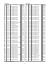
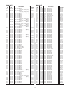
6 - 3 m.=mounted side (t: mounted on the top side, b: mounted on the bottom side) [main unit] ref order description m. H/v no. No. Location [main unit] ref order description m. H/v no. No. Location r235 7030005090 s.Res erj2gej 104 x (100 k Ω) b 20.3/4.2 r236 7030005230 s.Res erj2gej 334 x (330 k Ω)...
Page 22
S.=surface mount 6 - 4 m.=mounted side (t: mounted on the top side, b: mounted on the bottom side) [main unit] ref order description m. H/v no. No. Location [main unit] ref order description m. H/v no. No. Location c114 4030017360 s.Cer ecj0ec1h030b t 51.9/36.5 [us3], [ge3], [us3s], [ge3s] 403001758...
Page 23
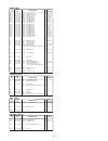
6 - 5 [main unit] ref order description m. H/v no. No. Location [chassis unit] ref order description m. H/v no. No. Location c324 4030017420 s.Cer ecj0ec1h470j t 85/13.7 c325 4550006250 s.Tan teesva 1a 106m8l t 90.6/17.2 c326 4510006940 s.Ele eevfc0j101p b 87.8/8.9 c333 4030017420 s.Cer ecj0ec1h470j...
Page 24
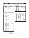
Section 7 mechanical parts and disassembly 7 - 1 screw abbreviations b0, bt: self-tapping zk: black sus: stainless ni-zu: nickel-zinc 7-1 cabinet parts [main unit] [chassis parts] mp4 ep2 mp1 mp2 mp3 ep1 [accessories] ref. Order. No. Description qty. Ep1 3310002311 fa-sc25u-1 [us2], [us2s], [eu2] 1 ...
Page 25
7 - 2 unit abbreviation (c): chassis parts, (m): main unit a a mp25(c) * mp11(c) mp10(c) mp9(c) mp33(c) mp20(c) sp1(c) main unit mp28(c) mp28(c) mp5(m) mp28(c) mp28(c) mp21(c) mp22(c) mp34(c) mp28(c) mp16(c) mp28(c) * s4(m) r226(m) connect unit mp29(c) mp30(c) ant unit mp1(c) j1(c) * mp36(c) mp35(c)...
Page 26
Section 8 semi-conductor information 8 - 1 • transistors and fets 2sa2048tl r (symbol: ul) 2sb1132 r (symbol: barb) b e c b c e 2sc4116 bl (symbol: ll) e c b 2sc4226 r25 (symbol: br) e c b 2sc5107 o (symbol: mfo) e c b 2sk1829 (symbol: k1) s d g unr911hj (symbol: 6p) 2sk880 y (symbol: xy) s d g 3sk2...
Page 27
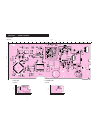
Ic14 r258 q3 4 ic6 ic10 t5v ic7 q3 5 ic13 r265 r261 ic5 q32 q22 s5v c356 c211 c279 x2 ic8 l33 l35 ic 4 d24 q1 9 ck st r5v ch +5 j5 sp cl mi c g sp q2 3 ic12 f1 ds1 f1 q6 q2 4 g q2 5 l29 d22 d16 d21 c148 q17 lv l26 q1 4 l40 q10 d25 d15 q1 q8 c18 c179 l15 bo ard q7 r56 c325 q30 j1 q31 q21 d14 l20 ic2 ...
Page 28
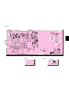
15 1 opv1 opv2 dast gnd opt3 opt2 opt1 sigo nmi busy res mcin mcot ptt ptti 16 30 sck si so cirq ccs cp10 disc det cp11 beepo afono cp12 vcc +5v gnd j4 to the optional unit c175 c3 c4 c186 r2 d1 c5 c8 c229 c238 r238 c230 c227 c309 r221 c265 c306 c307 c167 c58 c67 r39 c168 c169 r223 c311 r222 c266 r2...
Page 29
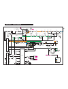
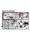
Section 10 block diagram 10 - 1 notes : contorol line common line tx line rx line data lime voltage line bal x2: cr-783 15.3 mhz q19: 2sc4116 ref x3 bpf pll ic ic4: mb15a02 tcxo lvin s5v loop fil ripple fil buff 45.9 mhz sql in det mod lva, t1, t2 d/a fm if ic ic8: m62363fp q14: 2sc4226 d16: hvc350b...
Page 30
Section 11 voltage diagram 11 - 1 11-1 main unit c130 0.047 d16 hvc350b c354 0.001 voltage line notes : common line tx line rx line vcc c211 4.7 r103 47 k c159 0.001 ep3 c158 0.1 cp1 c143 0.001 c141 0.001 r100 4.7 k r101 470 r92 120 k c137 0.01 c203 0.001 d22 hvc370b c115 12 p 4 p c134 15 p 12 p c11...
Page 31
Asia icom inc. 6f no.68, sec. 1 cheng-teh road, taipei, taiwan, r.O.C. Phone : +886 (02) 2559 1899 fax : +886 (02) 2559 1874 url : http://www.Asia-icom.Com e-mail : sales@asia-icom.Com zac de la plaine, 1, rue brindejonc des moulinais bp 5804, 31505 toulouse cedex, france phone : +33 (5) 61 36 03 03...
Page 32
1-1-32, kamiminami, hirano-ku, osaka, 547-0003, japan s-14116iz-c1 © 2004 icom inc..

