- DL manuals
- Icom
- Two-Way Radio
- IC-F40GS
- Servise Manual
Icom IC-F40GS Servise Manual
Summary of IC-F40GS
Page 1
Uhf transceiver ic-f40gt ic-f40gs ic-f4 1 gt ic-f4 1 gs ic-f40gt ic-f40gs ic-f41gt ic-f41gs s-13803mz-c1-q © 2001 icom inc. 1-1-32, kamiminami, hirano-ku, osaka 547-0003, japan ( including mt version ).
Page 2
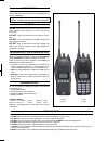
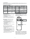
Introduction this service manual describes the latest service information for the ic-f40gt/gs and ic-f41gt/gs uhf transceiver at the time of publication. To upgrade quality, all electrical or mechanical parts and inter- nal circuits are subject to change without notice or obligation. Danger never co...
Page 3
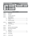
L-band 400–430 mhz m-band ml-band 440–480 mhz mh-band 450–490 mhz h-band h1-band 480–512 mhz h2-band 480–520 mhz table of contents explicit definitions section 1 specifications section 2 inside views section 3 disassembly instructions section 4 circuit description 4 - 1 receiver circuits ..............
Page 4: Section 1
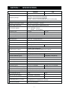
Measurement method frequency coverage type of emission number of conventional channels power supply requirement current drain (approx.) frequency error usable temperature range dimensions (proj. Not included) weight (with bp-210) rf output power modulation system maximum permissible deviation spurio...
Page 5: Section 2
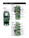
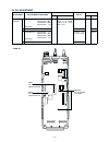
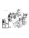
2 - 1 section 2 inside views • front unit bottom view • main unit top view • main unit bottom view key led switch (q1, q2: 2sc4116bl) lcd module (ds10: edmmud1fa0) internal speaker switch circuit (q6, q7: cph3403, q8: 2sc4081, q9: dtc144eua) expander ic (ic1: tc74vhc373ft) power detector (d2, d3: rb...
Page 6: Section 3
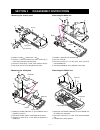
3 - 1 section 3 disassembly instructions 1 removing the chassis panel 2 removing the shield plate 3 removing the main unit 4 removing the front unit q remove 2 knobs a , and unscrew 1 nut b. W unscrew 1 screw c (icom screw), and 2 screws d (2 × 4 mm, black) from the 9-pin connector. E unscrew 2 scre...
Page 7: Section 4
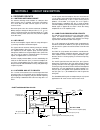
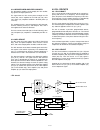
4-1 receiver circuits 4-1-1 antenna switching circuit the antenna switching circuit functions as a low-pass filter while receiving and a resonator circuit while transmitting. This circuit does not allow transmit signals to enter the receiver circuits. Received signals enter the antenna connector (ch...
Page 8
4 - 2 4-1-5 af amplifier circuit the af amplifier circuit amplifies the demodulated af sig- nals to drive a speaker. The af signals from the fm if ic (ic3, pin 9) are amplified at the af amplifier section of the compander ic (ic9, pins 5, 4) and are then applied to the high-pass filter circuit (ic10...
Page 9
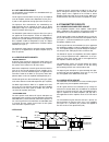
4 - 3 4-2-3 drive/power amplifier circuits the drive/power amplifier circuits amplify the vco oscillat- ing signal to an output power level. The signal from the vco circuit passes through the t/r switch (d4), and is amplified at the ygr (q5, q3), drive (q2), power (q1) amplifiers to obtain 4 w of rf...
Page 10
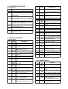
4 - 4 4-4 power supply circuit voltage line 4-5 port allocations 4-5-1 cpu (ic14) 4-5-2 i/o expander (ic23) line hv vcc cpu5v +5v s5v t5v r5v description the voltage from the attached battery pack. The same voltage as the hv line (battery volt- age) which is controlled by the power swtich ([vol] con...
Page 11
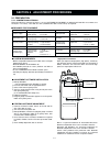
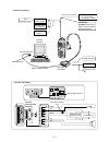
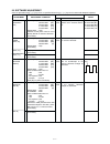
5 - 1 5-1 preparation 5-1-1 conventional version when you adjust the contents on pages 5-7 to 5-9, software adjustment, the optional cs-f30g adj adjustment soft- ware (rev. 1.0 or later), *opc-966 jig cable (modified opc-966 cloning cable ) are required. ■ required test equipment section 5 adjustmen...
Page 12
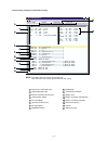
5 - 2 cs-f30g adj rev.1.0 file com 1: open option connect reload (f5) disp para [a / d] vin : 197 : c5h : 7.73 v temps : 190 : beh : 32.23 'c lvin : 67 : 43h : 1.31 v sd : 27 : 1bh : 0.53 v bdet : 0 : 00h : 0.00 v (ni-cd, ni-mh) power (hi) : 98 [ # # # # # # # # – – – – – – – – – – – ] power (l2) : ...
Page 13
5 - 3 5-1-2 mpt version when you adjust the contents on pages 5-7 to 5-9 software adjustment, the optional cs-f40g adj adjustment soft- ware (rev. 1.0 or later), *opc-966 jig cable (modified opc-966 cloning cable ) are required. And all adjustments in this sec- tion must be performed at conventional...
Page 14
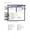
5 - 4 cs-f40g adj rev.1.0 file com 1: open option connect reload (f5) disp para [a / d] vin : 197 : c5h : 7.73 v temps : 190 : beh : 32.23 'c lvin : 67 : 43h : 1.31 v sd : 27 : 1bh : 0.53 v bdet : 0 : 00h : 0.00 v (ni-cd, ni-mh) power (hi) : 98 [ # # # # # # # # – – – – – – – – – – – ] power (l2) : ...
Page 15
5 - 5 + + – audio generator 300 hz to 3 khz ac millivoltmeter sp+ sp– mice mic ptt ptte add a jumper wire here • *opc-966 (jig cable) electrolytic capacity 47 µf opc-966 (cloning cable) sinad meter speaker (8 Ω) audio generator • connection (common) to the antenna connector rf power meter 0.1–10 w/5...
Page 16
5 - 6 5-2 pll adjustment pll lock voltage 1 2 3 4 • operating freq. : 400.000 mhz [l] 440.000 mhz [ml] 450.000 mhz [mh] 480.000 mhz [h] • receiving • transmitting • operating freq. : 430.000 mhz [l] 480.000 mhz [ml] 490.000 mhz [mh] 520.000 mhz [h] • receiving • transmitting main connect a digital m...
Page 17
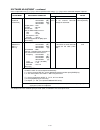
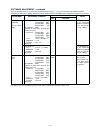
5 - 7 5-3 software adjustment select an operation using [ ↑] / [↓] keys, then set specified value using [←] / [→] keys on the connected computer keyboard. 1 1 2 3 1 1 2 • operating freq. : 430.000 mhz [l] 480.000 mhz [ml] 490.000 mhz [mh] 512.000 mhz [h1] 520.000 mhz [h2] • output power : low1 • con...
Page 18
5 - 8 *the output level of the standard signal generator (ssg) is indicated as the ssg’s open circuit. Note: after “rx sensitivity” adjustment is finished, “s-meter (or rssi l0/l2—[mpt])” adjustment (at page 5-9) must be re-adjusted. Software adjustment – continued select an operation using [ ↑] / [...
Page 19
5 - 9 software adjustment – continued select an operation using [ ↑] / [↓] keys, then set specified value using [←] / [→] keys on the connected computer keyboard. “s-meter (or rssi l0/l2—[mpt])” adjustment must be performued after “rx sensitivity” adjustment (at page 5-8) is finished. *the output le...
Page 20: Section 6
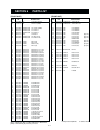
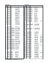
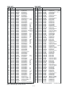
[front unit] [front unit] ic1 1130009860 s.Ic tc74vhc373ft (el) ic2 1110002750 s.Ic ta75s01f (te85r) q1 1530002850 s.Transistor 2sc4116-bl (te85r) q2 1530002850 s.Transistor 2sc4116-bl (te85r) q3 1590002150 s.Transistor dtc144te tl q4 1590002150 s.Transistor dtc144te tl q5 1590002150 s.Transistor dt...
Page 21
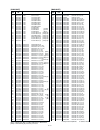
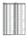
[main unit] [main unit] ic1 1130009130 s.Ic sa7025dk-t ic2 1130008560 s.Ic tc75s51f (te85l) ic3 1110003490 s.Ic ta31136fn (d, el) ic4 1130008560 s.Ic tc75s51f (te85l) ic5 1110001810 s.Ic ta7368f (tp1) ic6 1110002750 s.Ic ta75s01f (te85r) ic7 1110002750 s.Ic ta75s01f (te85r) ic8 1130008560 s.Ic tc75s...
Page 22
[main unit] [main unit] l40 6200009220 s.Coil lqw18an15ng00d l41 6200003590 s.Coil exccl3225u1 l42 6200004950 s.Coil nl 252018t-1r8j l43 6200002860 s.Coil nl 252018t-4r7j l44 6200001980 s.Coil nl 252018t-1r0j l45 6200004660 s.Coil mlf1608a 1r8k-t l46 6200004780 s.Coil mlf1608a 1r5k-t l47 6200001980 ...
Page 23
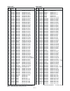
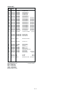
[main unit] [main unit] r151 7030005100 s.Resistor erj2gej 154 x (150 k Ω) r152 7030005310 s.Resistor erj2gej 124 x (120 k Ω) r153 7030009320 s.Resistor erj2gej 4r7 x (4.7 Ω) r155 7030007350 s.Resistor erj2gej 393 x (39 k Ω) r157 7030005220 s.Resistor erj2gej 223 x (22 k Ω) r159 7030005090 s.Resisto...
Page 24
[main unit] [main unit] r357 7030005120 s.Resistor erj2gej 102 x (1 k Ω) r358 7030005120 s.Resistor erj2gej 102 x (1 k Ω) r359 7030005120 s.Resistor erj2gej 102 x (1 k Ω) r360 7030005120 s.Resistor erj2gej 102 x (1 k Ω) r361 7030005720 s.Resistor erj2gej 563 x (56 k Ω) r362 7030005210 s.Resistor erj...
Page 25
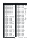
[main unit] [main unit] c118 4030013850 s.Ceramic ecue1e102kbq c121 4030016930 s.Ceramic ecj0eb1a104k c123 4030014200 s.Ceramic ecue1h101jcq c124* 4550006700 s.Tantalum ecst1ay106r c125 4030014200 s.Ceramic ecue1h101jcq c126 4030014220 s.Ceramic ecue1e471kbq c127* 4550006170 s.Tantalum ecst1ay225r c...
Page 26
[l]: l-band, [ml]: ml-band, [mh]: mh-band, [h]: h-band, [m]: ml and mh bands, [gt]: ic-f40gt/f41gt, [gs]: ic-f40gs/f41gs, [f40g]: ic-f40gt/f40gs, [f41g]: ic-f41gt/f41gs, [is]: intrinsically safe version *=safety critical components s.=surface mount [main unit] [main unit] c275 4030014180 s.Ceramic e...
Page 27
[main unit] c451 4030016930 s.Ceramic ecj0eb1a104k c452 4030016930 s.Ceramic ecj0eb1a104k c453 4030014140 s.Ceramic ecue1h150jcq c454 4030014240 s.Ceramic ecue1h180jcq c455 4030016930 s.Ceramic ecj0eb1a104k c456 4030016930 s.Ceramic ecj0eb1a104k c457 4030014070 s.Ceramic ecue1h040bcq c458 4030014200...
Page 28: Section 7
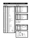
7 - 1 section 7 mechanical parts and disassembly mp1 8210017211 2337 front panel-1 assembly [gt] 1 8210017350 2337 s-front panel assembly [gs] 1 mp2 8310049450 2337 window plate 1 mp4 8930052850 2337 release button 1 mp5 8930052970 2337 ptt plate 1 mp8 8210017100 2337 rear panel 1 mp9 8210017080 233...
Page 29
7 - 2 note (m): main unit ( f ): front unit (c): chassis parts front unit main unit mp1 (c) mp1 (c) mp2 (c) mp58 (c) mp29 (c) mp13 (c) ds10 (f) sp1 (f) mp9 (c) mp51 (c) ic-f40gs and ic-f41gs parts ic-f40gt and ic-f41gt parts mp50 (c) mp22 (c) mp37 (c) mp61 (c) mp19 (c) mp26 (c) mp20 (c) mp5 (c) mp57...
Page 30
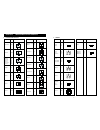
8 - 1 section parts list section 8 semi-conductor information 8 - 1 transistors and fets 8 - 2 diodes name symbol inside view 1ss355 a 1sv307 tx a c 1ss375 fh ma742 m1u rb706f-40 3j hsu88trf 9 ma111 1b ma2s111 a a c a c dan202u n c a1 a2 ma8030-h 3^0 ma8033-h 3^3 ma8062-m 6-2 a c dap202u p a1 c2 c1 ...
Page 31
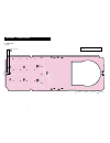
Surface inside 1 inside 2 under side 1 p0 p1 p2 p3 4 7 2 5 8 0 3 6 9 # ✽ microphone 9 - 1 9 - 1 front unit section 9 board layouts • top view the combination of this page and the next page shows the unit layout in the same configuration as the actual p.C. Board..
Page 32
Surface inside 1 inside 2 under side gnd spcn d0 frst ptt d5 d4 d3 d2 d1 rdb wrb rs gnd resb vcc kr0 kr1 kr2 kr3 mic+ sp+ gnd +5v d7 d6 nc d6 vr1 vee3 nc d1 d2 d3 d4 d5 d7 osc0 osc1 vss pmode vdd vee cap– cap+ vee2 1 5 10 15 20 25 30 35 40 vout vr2 scl wrb rdb d0 m86 vs/te resb csb rs m/s p/s v1 v2 ...
Page 33
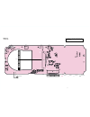
Under side inside-2 inside-1 surface s1 cp1 cp3 cp2 ant battery+ r193 gnd spcn d0 frst ptt d5 d4 d3 d2 d1 rdb wrb rs gnd resb vcc kr0 kr1 kr2 kr3 mic+ sp+ gnd +5v d7 d6 to front unit j1 1 26 8 7 2 4 5 6 9 afo vcc detect mice reset xrxd xtxd mic ptt 3 1 8 7 2 4 5 6 9 3 1 1 2 3 4 5 6 int sp sw af vr p...
Page 34
Under side inside-2 inside-1 surface s1 cp3 r193 8 7 2 4 5 6 9 3 1 8 7 2 4 5 6 9 3 1 1 2 3 4 5 6 int sp sw af vr power sw ch select ptt mic xtxd xrxd reset mice detect vcc afo mp67 (chassis)... [h-band] only f40g (main unit) • bottom view the combination of this page and the previous page shows the ...
Page 35
Under side inside-2 inside-1 surface s1 cp1 cp3 cp2 ant battery+ r193 8 7 2 4 5 6 9 afo vcc detect mice reset xrxd xtxd mic ptt 3 1 8 7 2 4 5 6 9 3 1 1 2 3 4 5 6 int sp sw af vr power sw ch select opt2 opt1 1 5 10 15 16 20 25 30 1 5 10 15 16 20 25 30 universal connector mp6 opc-966 em-80 ad-52 hs-93...
Page 36
Under side inside-2 inside-1 surface s1 cp3 r193 8 7 2 4 5 6 9 3 1 8 7 2 4 5 6 9 3 1 1 2 3 4 5 6 int sp sw af vr power sw ch select ptt mic xtxd xrxd reset mice detect vcc afo f41g (main unit) • bottom view the combination of this page and the previous page shows the unit layout in the same configur...
Page 37
10 - 1 section 10 block diagram 400-520 mhz d2,d3 rb706f-40 q1 2sk2974 d1: d24, d25: 1sv307 ma77 q2 2sk2973 q3 2sc3585 main unit main unit q5 2sc5107 vco sw vcos d4, d5: ma77 q6 2sc5107 q8 2sc5107 q9: dtc144eu q10: xp1214 rx vco q13 2sc4116 q11 2sc4226 s5v lvin buff q14 2sk880 ic1 sa7025 x1 cr-667 i...
Page 38
11 - 1 note [f40g]: ic-f40gt/f40gs [ gt] : ic-f40gt/f41gt [l] : l-band 400–430 mhz [h] : h-band 480–512/480–520 mhz [ f41g]: ic-f41gt/f41gs [ gs] : ic-f40gs/f41gs [ml] : ml-band 440–480 mhz [m] : ml and mh bands [mh] : mh-band 450–490 mhz opv21 opv22 opv23 fclr mske rgs2 w5 d6 d7 +5v gnd sp+ mic+ kr...
Page 39
11 - 1 note [f40g]: ic-f40gt/f40gs [ gt] : ic-f40gt/f41gt [l] : l-band 400–430 mhz [h] : h-band 480–512/480–520 mhz [ f41g]: ic-f41gt/f41gs [ gs] : ic-f40gs/f41gs [ml] : ml-band 440–480 mhz [m] : ml and mh bands [mh] : mh-band 450–490 mhz opv21 opv22 opv23 fclr mske rgs2 w5 d6 d7 +5v gnd sp+ mic+ kr...
Page 40
11 - 1 note [f40g]: ic-f40gt/f40gs [ gt] : ic-f40gt/f41gt [l] : l-band 400–430 mhz [h] : h-band 480–512/480–520 mhz [ f41g]: ic-f41gt/f41gs [ gs] : ic-f40gs/f41gs [ml] : ml-band 440–480 mhz [m] : ml and mh bands [mh] : mh-band 450–490 mhz opv21 opv22 opv23 fclr mske rgs2 w5 d6 d7 +5v gnd sp+ mic+ kr...
Page 41
Introduction this service manual describes the latest service information for the ic-f40gt/gs and ic-f41gt/gs uhf transceiver at the time of publication. To upgrade quality, all electrical or mechanical parts and inter- nal circuits are subject to change without notice or obligation. Danger never co...
Page 42: ( Including
Uhf transceiver ic-f40gt ic-f40gs ic-f4 1 gt ic-f4 1 gs ic-f40gt ic-f40gs ic-f41gt ic-f41gs s-13803mz-c1-q © 2001 icom inc. 1-1-32, kamiminami, hirano-ku, osaka 547-0003, japan ( including mt version ).

