- DL manuals
- Icom
- Transceiver
- IC-F5122D
- Service Manual
Icom IC-F5122D Service Manual
Summary of IC-F5122D
Page 1
S-14713xz-c1 feb. 2011 vhf mobile transceivers.
Page 2
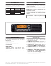
This service manual describes the latest technical information for the ic-f5121d, ic-f5122d and ic-f5123d vhf transceivers, at the time of publication. Never connect the transceiver to an ac outlet or to a dc power supply that uses more than the specified voltage. This will ruin the transceiver. Do ...
Page 3
Table of contents section 1 specifications section 2 inside views section 3 disassembly instruction section 4 optional cable installation section 5 circuit descripiton 5-1 receiver circuits. . . . . . . . . . . . . . . . . . . . . . . . . . . . . . . . . . . . . . . . . . . . . . . . . . . . . . . ....
Page 4: Section 1. Specifications
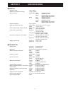
1 - 1 section 1. Specifications m general • frequency range : 136–174 mhz • number of conventional channels : 128 ch (8 zones) • type of emission : [usa], [exp] wide 16k0f3e (25.0khz) narrow 11k0f3e (12.5khz) digital 8k10f1d/8f10f1e (12.5khz) 4k00f1d/4f00f1e (6.25khz) [eur] wide 16k0f3e (25.0khz) mi...
Page 5
1 - 2 m receiver • sensitivity : [usa], [exp] 0.25 µv typ. At 12 db sinad [eur] –4 dbµv (emf) typ. At 20 db sinad • squelch sensitivity (at threshold) : [usa], [exp] 0.25 µv typ. [eur] –4 dbµv (emf) typ. • intermediate frequency : 1st if; 46.35 mhz, 2nd if; 450 khz • adjacent channel selectivity : n...
Page 6: Section 2. Inside
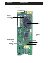
2 - 1 section 2. Inside views • front unit cpu (ic51) lcd driver (ic6) mic amp (ic7) mic gain sw (ic53) eeprom (ic52) clock frequency shift diode (d60) cpu clock (x51) backlight sw (q5) dimmer controller (q2) mic amp frequency response sw (ic54) backlight led driver (q1).
Page 7
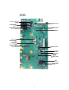
2 - 2 • main unit (top view) 2nd if amp (for digital mode) (ic5) af mute sw (ic1008) alc/hpf (ic1005) dsp (ic2007) linear codec (ic2006) if demodulator ic (ic4) +3 line regulator (q1017) ripple filter (q2 ) vco sw (q10) hv line switch (q1003) +8v line regulator (ic1002) r8 line sw (q1013) apc amp (i...
Page 8
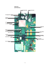
2 - 3 • main unit (bottom view) vco analog/digital af line sw (ic1008) af amp (ic1004) reference frequency oscillator (x2) +3v line regulator (ic1001) af amp (ic6) electronic volume ic (ic1006) idc, af amp, hpf (ic1007) pll ic (ic8) drive amp (q17) 1st if mixer (q19) 2nd if filter (for wide mode) (f...
Page 9: Section 3. Disassembly
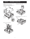
3 - 1 section 3. Disassembly instruction flat cable bottom cover screw×4 front panel speaker cable unsolder solder remover main unit main unit chassis main unit screw×9 1) remove 4 screws from the bottom cover, and then remove it. 2) disconnect the fl at cable and speaker cable. 3) remove 2 screws f...
Page 10: Section 4
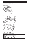
4 - 1 section 4 optional cable installation install optional opc-1939/opc-2078 as follows: 1) turn off the power, and then disconnect the dc power cable. 2) unscrew 4 screws, then remove the bottom cover. 3) install the cable as shown. Opc-1939/opc-2078 cut off the bushing as in the illustration. K ...
Page 11: Section 5. Circuit
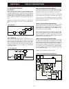
5 - 1 section 5. Circuit description 5-1 receiver circuits rf circuits the rx signal from the antenna is passed through the lpf and antenna sw (d24–d26, d28, d32), then fi ltered by the 2-staged tuned bpfs (d31 and d37) to eliminate unwanted out-of-band signals. The fi ltered rx signal is amplifi ed...
Page 12
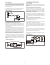
5 - 2 rx af circuits the demodulated af signal from the linear codec (ic2006) is amplified by the af amp (ic1007), and then adjusted in level by the electronic volume (ic1006). The level-adjusted af signal is then amplifi ed by the pre-amp (ic1004) and af power amp (ic1009). The amplified af signal ...
Page 13
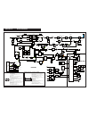
5 - 3 lo sw d15,d16 q7,d6,d7 modulation fm:analog 4fsk:digital d10 buff q15 buff q12 tx vco from the tx af circuits to the tx amp circuits mod lpf pwr det d27,d29,d35 mute sw q23 ant sw d24-d26, d28,d32 pwr am p ic3 apc amp ic2 drive amp q17 t1 tmut ant from the tx vco to the rx circuits lpf lpf lo ...
Page 14
5 - 4 5-5 port allocations • cpu (front unit: ic51) • d/a converter (ic1006) pin no. Line name description 23 t1 (txpo) during receiving: o u t p u t s b p f t u n i n g voltage. During transmitting: tx power reference voltage. 24 t2 outputs bpf tuning voltage 7 ref outputs reference frequency adjus...
Page 15: Section 6. Adjustment
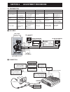
6 - 1 section 6. Adjustment procedure ¤ connection ¤ jig cable 6-1 preparation equipment grade and range equipment grade and range cloning software cs-f3100d/f5120d : revision 1.0 or later jig cable modifi ed opc-1122u (see the illust below) dc power supply output voltage current capacity : 13.6 v d...
Page 16
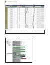
6 - 2 ¤ adjustment channels for [eur] versions: when adjusting “deviation” in the middle band, change the bandwidth to “middle” as shown. Select “middle” convenient: the cloning data fi le for the adjustment, as described in this service manual, is attached. Right click the clip icon, and select “sa...
Page 17
6 - 3 ¤ adjustment utility adjustment condition reference frequency tx output power squelch sensitivity pll lock voltage (rx) pll lock voltage (tx) ctcss deviation dtcs deviation modulation balance modulation balance (preset) digital deviation fm deviation s-meter 2/5 tone deviation.
Page 18
6 - 4 adjustment transceiver’s condition operation adjustment item value pll lock voltage (rx) 1 • channel : 1-1 • receiving 1) connect an rf power meter to the antenna connector. 2) set the adjustment value on the "adjust utility" screen. [rx lva(adjust)] 1.1 v (tx) 2 • channel : 1-2 • transmitting...
Page 19
6 - 5 no over or under shoot. As flat as possible. Adjustment transceiver’s condition operation adjustment item value tx power (hi power) 1 • channel : 1-6 • transmitting • connect an rf power meter to the antenna connector. [power (hi)] 50 w [50 w ver.] 25 w [25 w ver.] (l2 power) 2 • channel : 1-7...
Page 20
6 - 6 adjustment transceiver’s condition operation adjustment item value digital deviation (band low) 1 • channel : 1-21 • transmitting 1) set the tx mode to "16" on the "adjust utility" screen. 2) push [enter] on the pc’s keyboard, to enter the digital deviation adjustment mode. [mod d start] – 2 •...
Page 21
6 - 7 6-4 receive adjustments 1) select an adjustment item using [ ↑]/[↓] on the pc's keyboard. 2) set or modify the adjustment value as specifi ed using [ ←]/[→] on the pc's keyboard, then push [enter]. Adjustment transceiver’s condition operation adjustment item value rx sensitivity 1 note: when "...
Page 22: Section 7
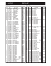
7 - 1 section 7 parts list ic2 1110002751 s.Ic ta75s01f(te85rf) t 60/54.9 ic3 1150002423 ic ra60h1317m1a-222 ic4 1110007320 s.Ic njm2591v-te1-#zzzb t 57.8/24.7 ic5 1110006230 s.Ic njm2711f-te1-#zzzb t 36.0/26.9 ic6 1110002751 s.Ic ta75s01f(te85rf) b 59.9/17.4 ic7 1130011741 s.Ic tc7w66fk(te85lf) t 8...
Page 23
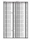
7 - 2 ref parts description m. H/v no. No. Location [main unit] r14 7030005050 s.Res erj2gej 103 x (10k) b 31.9/35.5 r15 7030005700 s.Res erj2gej 274 x (270k) b 39.2/38.6 r16 7030008280 s.Res erj2gej 271 x (270) b 39.5/40.7 r17 7030004980 s.Res erj2gej 101 x (100) b 51.5/40.2 r19 7030005090 s.Res er...
Page 24
7 - 3 ref parts description m. H/v no. No. Location [main unit] r1082 7410001130 s.Arr exb28v102jx t 56.9/6.7 r1083 7030005120 s.Res erj2gej 102 x (1k) b 69.1/8.8 r1084 7410001130 s.Arr exb28v102jx t 61.7/6.1 r1085 7030005120 s.Res erj2gej 102 x (1k) t 65.8/6.1 r1086 7030008310 s.Res erj2gej 564 x (...
Page 25
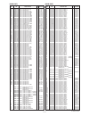
7 - 4 ref parts description m. H/v no. No. Location [main unit] c123 4030017420 s.Cer c1005 ch 1h 470j-t b 105.0/29.2 c124 4030017440 s.Cer c1005 ch 1h 221j-t b 106.0/26.2 c126 4030017390 s.Cer c1005 ch 1h 180j-t b 97.9/25.3 c127 4030017640 s.Cer c1005 ch 1h 150j-t b 93.9/23.3 c129 4030017340 s.Cer ...
Page 26
7 - 5 ref parts description m. H/v no. No. Location [main unit] c1070 4030017440 s.Cer c1005 ch 1h 221j-t b 120.4/16.2 c1071 4030016930 s.Cer c1005 jb 1a 104k-t b 120.4/10.8 c1074 4030017460 s.Cer c1005 jb 1h 102k-t b 73.9/10.4 c1075 4030017460 s.Cer c1005 jb 1h 102k-t b 70.7/14.4 c1076 4030017460 s...
Page 27
7 - 6 ref parts description m. H/v no. No. Location [front unit] ic6 1130015530 s.Ic bu9795akv-e2 b 43.0/21.2 ic7 1110002751 s.Ic ta75s01f(te85rf) b 28.3/24.7 ic51 1140015010 s.Ic hd64f2506rbr26dv(empty) b 67.5/21.9 ic52 1130015080 s.Ic r1ex24512asas0a b 92.3/15.4 ic53 1130011741 s.Ic tc7w66fk(te85l...
Page 28: Section 8. Mechanical
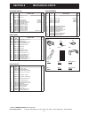
8 - 1 [chassis parts] ref order description qty. No. No. J1 6510004880 mr-ds-e 01 1 w1 8900011800 opc-1199 1 mp1 8010019065 2601 chassis-5 [eur-01] 1 8010019065 2601 chassis-5 [exp-01] 1 8010019135 2601 long chassis-5 [usa-01] 1 8010019135 2601 long chassis-5 [exp-02] 1 mp2 8110007821 2601 cover-1 r...
Page 29
8 - 2 mp8 (c) mp8 (c) r14 (f) j1 (f) mp10 (f) mp12 (f) ep2 (f) w1 (f) w1 (c) mp3 (f) front unit unit abbreviations (f): front unit (m): main unit (c): chassis parts mp5 (f) mp9 (f) ds11 (f) mp6 (f) mp1 (f) sp1 (f) mp11 (f) mp5 (c) ×2 mp3 (m) mp1 (c) mp1 (c) [50 w version] [25 w version] j1 (c) mp4 (...
Page 30
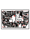
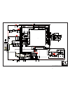
9 - 1 section 9. Board layouts the combination of top side and bottom side of this • front unit (top view) c9 c10 c12 c128 c129 d1 d2 ds1 ds2 ds3 ds4 ds5 ds6 ds7 ds8 ds9 j1 r14 r14 r18 r76 h0 h5 h10 h15 h20 h25 h30 h35 h40 h45 h50 h55 h60 h65 h70 h75 h80 h85 h90 h95 v0 v5 v10 v15 v20 v25 v30
Page 31
9 - 2 the combination of top side and bottom side of this • front unit (bottom view) 8v nc nc eptt igsw sso dmiso sck nwc ads dss dmosi afon mic tmut nois rxc txc unlk plst dres beep pwon dast dsirq horn plsw dsck (rxd0) batv temp lvin rssi cres cpu3.3v pgio4 dpdn gnd gnd afo md2 cres cpu3.3v gnd gn...
Page 32
9 - 3 the combination of top side and bottom side of this • main unit (top view) nwc igsw nc gnd sck horn rssi pgio3(txd0) tmut pgio4 lvin dsck dmiso mic 8v dmosi beep dres dss rxc sso cpu3.3v txc dast eptt pwon gnd plst unlk ads pgio2(rxd0) temp nois batv plsw afo afon dsirq cres dpdn ext.I/o 4 (se...
Page 33
9 - 4 the combination of top side and bottom side of this [ext. Sp jack] • main unit (bottom view) ic3 c1 c2 c3 c4 c5 c6 c7 c8 c10 c11 c13 c14 c15 c17 c18 c19 c20 c22 c25 c26 c27 c28 c29 c30 c32 c33 c34 c35 c36 c37 c38 c39 c40 c41 c42 c43 c44 c45 c46 c48 c49 c50 c52 c53 c54 c57 c62 c64 c67 c74 c78 c...
Page 34
10 - 1 section 10. Block diagram lpf lpf lpf lpf pwr det d27:lrb706f d29:lrb706f ref x2 cr-892 mut e sw q23:ldtc114ye ant sw pwr am p ic3 ra30h1317m1a(25 w ver.) ra60h1317m1a(50 w ver.) lo sw hvd142a d15,d16 q6:2sc4226 d4:hvc376b d5:hvc376b q7:2sc4226 d7:hvc376b d6:hvc376b fil ripple q2 2sc4116 vco ...
Page 35
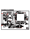
11 - 1 section 11. Voltage diagram *: refer to the parts list for the value and name of component. • front unit dim on 6.3v dim off 7.3v tx 0.0v rx 3.2v light on 3.2v light off 0.0v dim on 0.0v dim off 3.2v 3.2v 3.2v 8.0v 19.66mhz 2.3vp-p j1 1 2 3 4 5 6 7 8 *l1 q1 2sc4116 *l2 key s1 *r14 r16 1k *r15...
Page 36
11 - 2 • main unit (1/3) *: refer to the parts list for the value and name of component. 8.0v 5.0v 7.1v tx 3.0v rx 0.0v tx 2.3v rx 2.2v tx 0.0v rx 2.9v tx 6.7v rx 0.0v tx 8.0v rx 0.0v 50w4.9v 25w3.9v 13.6v tx 0.0v rx 3.0v 50w2.3v 25w1.6v tx 0.2v rx 1.4v tx 0.0v rx 6.5v tx 0.0v rx 5.7v tx 0.0v rx 3.9...
Page 37
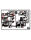
11 - 3 • main unit (2/3) *: refer to the parts list for the value and name of component. 13.6v 2.2v 13.6v power on 2.8v power off 0.0v 3.3v 1.9v 8.0v 8.0v tx 8.1v rx 0.0v tx 0.0v rx 7.9v 3.3v 5.0v 265mvrms 5.0v c1092 0.1 unlk c1026 1 c1135 0.001 c1132 0.001 c1053 10 d isc r1086 560k c1061 0.001 r8v ...
Page 38
11 - 4 • main unit (3/3) *: refer to the parts list for the value and name of component. 3.3v 1.5v 3.3v 12.28mhz 1.1vp-p 1.3v c2054 0.1 r2019 0 c2004 10 cp111 c2047 0.1 dmi c2051 0.1 c2055 22p +3.3v cp128 r2020 0 r2036 100 dmo c2015 0.1 c2036 1 c2016 47 i c2007 h11 l7 m7 k7 k6 p6 m6 l6 n5 l5 p4 n4 l...
Page 39
6f no.68, sec. 1 cheng-teh road, taipei, taiwan, r.O.C. Phone : +886 (02) 2559 1899 fax : +886 (02) 2559 1874 url : http://www.Asia-icom.Com e-mail : sales@asia-icom.Com zac de la plaine 1 rue brindejonc des moulinais bp 5804 31505 toulouse cedex, france phone : +33 (5) 61 36 03 03 fax : +33 (5) 61 ...
Page 40
1-1-32, kamiminami, hirano-ku, osaka 547-0003, japan s-14713xz-c1 © 2011 icom inc..

