- DL manuals
- Icom
- Transceiver
- IC-F6061
- Service Manual
Icom IC-F6061 Service Manual
Summary of IC-F6061
Page 1
S-14324xz-c1 feb. 2007 uhf transcevers.
Page 2
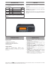
This service manual describes the latest service information for the ic-f6061/f6062/f6063 uhf transceivers at the time of publication. Never connect the transceiver to an ac outlet or to a dc power supply that uses more than 15 v. This will ruin the transceiver. Do not expose the transceiver to rain...
Page 3
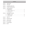
Contents section 1 specifications section 2 inside views section 3 disassembly instructions section 4 optional units installation section 5 circuit descripiton 5-1 receiver circuits. . . . . . . . . . . . . . . . . . . . . . . . . . . . . . . . . . . . . . . . . . . . . . . . . . . . . . . . 5-1 5-2...
Page 4: Section 1
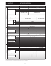
1 - 1 section 1 specifications [usa] [exp] [eur] general • frequency coverage 400–470 mhz [usa-01] 450–512 mhz [usa-02] 400–470 mhz [exp-01] 450–520 mhz exp-02] 400–470 mhz • type of emission wide 16k0f3e (25.0 khz) middle – 14k0f3e (20.0 khz) narrow 11k0f3e (12.5 khz) 11k0f7e/d (12.5 khz) 8k10f1e/d...
Page 5: Section 2
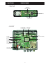
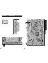
2 - 1 section 2 inside views if ic (ic170: ta31136fng) lcd driver (ic501: s1d15206f) front cpu (ic503: hd64f3687) front cpu clock (x501: cr-764) af switch/amp (ic1: njm12902v) bbic clock (x2: cr-765) af lpf (ic7: njm12902v) cpu clock (x5: cr-764) ref osc (x1: cr-826) pll ic (ic4: lmx2352tm) level co...
Page 6: Section 3
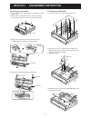
3 - 1 section 3 disassembly instruction 1. Removing the front panel q turn the transceiver’s power off, then disconnect the dc power cable w unscrew the 4 bottom screws, then remove the bottom cover from the transceiver in the direction of the arrow. 2. Removing the main unit q unscrew 7 screws a , ...
Page 7
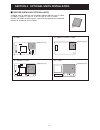
4 - 1 section 4 optional units installation a sponge with an adhesive strip has been added to optional units (ut-96r, ut-108r, ut-109r, ut-110r, ut-119r, ut-119h, ut-124, ut-124r). Remove the bottom protective papar, and attach the sponge to the specifi ed position on the optional units as below. P ...
Page 8
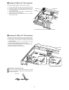
4 - 2 p optional ut-96r or ut-119h installation install the optional ut-96r or ut-119h unit as follows: q turn the power off, then disconnect the dc power cable. W unscrew the 4 cover screws, then remove the bottom cover. E install the ut-96r to j1 and the ut-119h to j2 as shown in the diagram below...
Page 9: Section 5
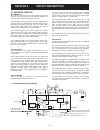
5 - 1 section 5 circuit description 5-1 receiver circuits rf circuits the antenna switching circuit toggles between the receive (rx) line and transmit (tx) line. Rf amplifi er amplifi es the received signals within the frequency coverage. Received signals from the antenna are passed through low pass...
Page 10
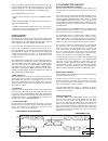
5 - 2 the processed af signals from the base band ic (ic2) are passed through the af mute switch (ic8, pins 3, 4) and d/a converter (ic6, pins 15, 16) for level adjustment. The level adjusted af signals are amplified by af amplifier (ic22). The amplified af signals are then; - output from d-sub 25 p...
Page 11
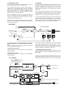
5 - 3 tx power amplifiers the transmit signal from the tx vco is amplified to the transmit output level by the transmit amplifi ers. The tx vco output signal from buffer amplifier (q29) is applied to the ygr amplifiers (q30, q53) via the tx/rx switch (d24). The amplified tx signal is passed through ...
Page 12
5 - 4 pll ic the pll circuit provides stable oscillation of the transmit frequency and receive 1st lo frequency. The pll output frequency is controlled by the divided ratio (n-data) from the cpu. The applied signals are divided at the prescaler and programmable counter according to the control signa...
Page 13
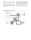
5 - 5 • cpu (main unit; ic14) pin no. Port name description 1 dsda outputs serial data to the d/a converter (ic20, pin 6). 2 dast outputs strobe signal to the d/a converter (ic4, pin 6). 3 side3 input port for [side3] key (s4). "low"=when the key is pushed. 4−7 cbi0−3 input ports for [rotary selecto...
Page 14: Section 6
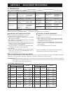
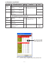
6 - 1 section 6 section 6 adjustment procedures 6-1 preparation when adjusting ic-f6060 series, cs-f5060 cloning software, cs-f5060 adj adjustment software (rev. 1.0 or later), opc-1122/u/ jig cable and the following test equipments are required. Equipment grade and range equipment grade and range d...
Page 15
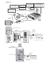
6 - 2 • connection modulation analyzer attenuator 50 db or 60 db to the antenna connector to dc cab le standard signal generator –127 to –17 dbm (0.1 v to 32 mv) caution: do not transmit while ssg is connected to the antenna connector. Rf power meter (50 Ω) 1–50 w [usa-01/02] 1–30 w [others] dc powe...
Page 16
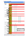
6 - 3 note : the above screen is an example only. Each transceiver has its own specific values for each setting. • adjustment software window transmit output power modulation balance fm deviation ctcss/dtcs deviation squelch level reference frequency rx sensitivity (auto.) rx sensitivity (manu.) pll...
Page 17
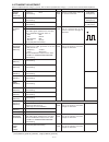
6 - 4 6-2 frequency adjustment select an adjustment item using [ ↑ ] / [ ↓ ] keys, then set to the specifi ed value using [ ← ] / [ → ] keys on the connected pc’s keyboard. Adjustment adjustment condition unit operation value pll lock voltage [rx lva1] 1 set the preset value of [lv (rx1)], [lv rx2] ...
Page 18
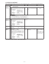
6 - 5 6-3 transmit adjustment select an adjustment item using [ ↑ ] / [ ↓ ] keys, then set to the specifi ed value using [ ← ] / [ → ] keys on the connected pc’s keyboard. Adjustment adjustment condition unit operation value output power [power (hi)] 1 • channel : ch 5 • transmitting rear panel conn...
Page 19
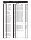
6 - 6 6-4 receive adjustment select an adjustment item using [ ↑ ] / [ ↓ ] keys, then set to the specifi ed value using [ ← ] / [ → ] keys on the connected pc’s keyboard. Adjustment adjustment condition unit location value receive sensitivity [bpf (t1)] [bpf (t2)] note: “receive sensitivity” must be...
Page 20: Section 7
7 - 1 section 7 parts list m.=mounted side (t: mounted on the top side, b: mounted on the bottom side) [front unit] ref order description m. H/v no. No. Location ic501 1130009121 s.Ic s1d15206f00a200 b 33.1/19.5 ic502 1110005771 s.Ic s-80942cnmc-g9ct2g b 61.4/9.7 ic503 1140010771 s.Ic hd64f3687fpv b...
Page 21
[low]=[usa-01], [exp-01], [eur-01] [high]=[usa-02], [exp-02] 7 - 2 m.=mounted side (t: mounted on the top side, b: mounted on the bottom side) [main unit] ref order description m. H/v no. No. Location ic1 1110005340 s.Ic njm12902v-te1-#zzzb t 82.3/12.9 ic2 1110006221 s.Ic ak2346p-e2/p b 44.7/11.7 ic...
Page 22
[low]=[usa-01], [exp-01], [eur-01] [high]=[usa-02], [exp-02] 7 - 3 m.=mounted side (t: mounted on the top side, b: mounted on the bottom side) [main unit] ref order description m. H/v no. No. Location l39 6200010150 s.Col as080340-15n t 14.3/60.3 l40 6200010150 s.Col as080340-15n t 10.3/82.4 l41 620...
Page 23
[low]=[usa-01], [exp-01], [eur-01] [high]=[usa-02], [exp-02] 7 - 4 m.=mounted side (t: mounted on the top side, b: mounted on the bottom side) [main unit] ref order description m. H/v no. No. Location r207 7030005050 s.Res erj2gej 103 x (10 k) t 120.3/37 r208 7030005050 s.Res erj2gej 103 x (10 k) t ...
Page 24
[low]=[usa-01], [exp-01], [eur-01] [high]=[usa-02], [exp-02] 7 - 5 m.=mounted side (t: mounted on the top side, b: mounted on the bottom side) [main unit] ref order description m. H/v no. No. Location c34 4030017570 s.Cer ecj0ec1h040b b 32/15.4 c35 4030017590 s.Cer ecj0ec1h070c b 30.8/15.9 c36 40300...
Page 25
[low]=[usa-01], [exp-01], [eur-01] [high]=[usa-02], [exp-02] 7 - 6 [main unit] ref order description m. H/v no. No. Location c236 4030017580 s.Cer ecj0ec1h060c [low] b 44.2/44.6 4030017620 s.Cer ecj0ec1h100c [high] b 44.2/44.6 c237 4030017620 s.Cer ecj0ec1h100c b 45.1/46 c239 4030017350 s.Cer ecj0ec...
Page 26
M.=mounted side (t: mounted on the top side, b: mounted on the bottom side) s.=surface mount [connect unit] ref order description m. H/v no. No. Location c601 4030017420 s.Cer ecj0ec1h470j t 12.7/4.6 c602 4030017420 s.Cer ecj0ec1h470j t 15.4/4.6 c603 4030017420 s.Cer ecj0ec1h470j t 18.2/4.6 c604 403...
Page 27: Section 8
Screw abbreviations a, b0, bt: self-tapping ph: pan head zk: black ni-zu: nickel-zinc sus: stainless 8 - 1 section 8 mechanical parts [chassis parts] ref order description qty. No. No. J1 6510004880 mr-dse-01 1 mp1 8010020540 2979 chassis 1 mp2 8930070860 o-ring (bm) 1 mp3 8110008960 2979 cover 1 mp...
Page 28
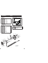
8 - 2 • exploded view 160 ( ) 161 ( ) 45 (1 25 / 32 ) 149.1 ( ) 15 ( 5 19 / 32 7 / 8 6 15 / 16 6 15 / 16 ) unit: mm (inch) front unit j1 (c) mp1 (c) mp10 (c) main unit black red unit abbreviations; (c) : chassis parts (f) : front unit (m) : main unit (cn) : connector unit mp501 (f) sp501 (f) mp505 (...
Page 29
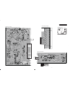
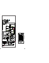
9 - 1 section 9 board layouts 0 2 5 c c527 c528 c539 d501 d502 d503 d508 d509 d510 ds502 ds503 ds504 ds505 6 0 5 s d ds507 ds508 ds509 ds510 ds511 ds512 ds513 3 0 5 j 7 0 5 r 8 0 5 r r522 r537 r538 r545 6 4 5 r r547 r548 r549 r560 0 h 5 h 0 1 h 5 1 h 0 2 h 5 2 h 0 3 h 5 3 h 0 4 h 5 4 h 0 5 h 5 5 h 0...
Page 30
9 - 2 c501 c502 c503 c504 c505 c506 7 0 5 c c508 9 0 5 c c510 1 1 5 c c512 c513 4 1 5 c c515 c516 c517 c518 c519 c521 c522 c523 c524 6 2 5 c 5 2 5 c c529 0 3 5 c c531 c533 4 3 5 c 5 3 5 c c536 c537 8 3 5 c c540 1 4 5 c 3 4 5 c 4 4 5 c 5 4 5 c 6 4 5 c 7 4 5 c c548 9 4 5 c c550 c551 c552 3 5 5 c c554 ...
Page 31
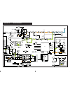
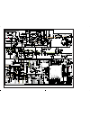
10 - 1 section 10 block diagram lp f pwr det d49,d51 ma728 ref x1 cr-826 mut e sw d 40:ma2s728 ant sw d39 l407cd (45w) pwr amp ic15 fil ripple q6 2sc4116 pll ic ic4 lmx2352tm x3 q3 2sc4116 x3 jtbm450cx24 bpf bpf bpf rf amp 3sk293 q31 apc am p ic17 ta75s01f if amp q12 2sc4215 buff q29 2sc5107 buff q2...
Page 32
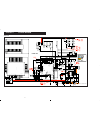
11 - 1 section 11 voltage diagram cf20 cp506 47p c545 1m r530 47p c539 sml-311yt ds511 cp508 0. 1 c503 ma2s111 d505 10k r557 2.2k r541 sml-311yt ds50 6 da221 d502 dn s507 47p c520 cf20 cp507 sml-311yt ds507 47k r525 22k r555 0.001 c553 0. 1 c549 dta114eu q50 3 cp509 100k r517 100k r559 p1 s502 100k ...
Page 33
11 - 2 njm12902v ic7 2 3 1 njm12902v ic7 6 5 7 njm12902v ic7 13 12 14 njm12902v ic7 9 10 8 njm12902v ic7 v+ 4 gnd 11 njm12902v ic1 2 3 1 njm12902v ic1 6 5 7 njm12902v ic1 9 10 8 njm12902v ic1 13 12 14 njm12902v ic1 v+ 4 gnd 11 120p c185 1.2u l6 0.001 c243 47 p c314 470 r26 unr9213j q34 100k r42 *c16...
Page 34
11 - 3 10k r305 dsa3a1 d62 4.7 r334 0.001 c377 10k r340 10k r347 1 c399 an78l05m ic18 i g as080340 l40 470 c412 ma728 d49 1k r337 0.001 c342 0.001 c393 0. 1 c390 1 c365 10k r307 *c349 100k r349 470 c411 0. 1 c351 0.001 c378 10 c338 *c345 5p c369 100k r342 *r297 3.3k r302 1 c368 330k r353 *c343 0.001...
Page 35
12 - 1 section 12 hm-152 [chassis parts] ref order description qty. No. No. W1 8900014230 opc-1471 1 w2 9028540010 awg24 l=70 gray 1 mp2 8210022100 2854 s-front panel 1 mp5 8210022120 2854 top panel 1 mp6 8930067080 2854 ptt button 1 mp7 8610012570 2854 sw button 1 mp8 8210022110 2854 side panel mp9...
Page 36
&.O3ec#heng4eh2oad4aipei4aiwan2/# 0hone &ax 52, httpwwwasiaicomcom %mailsales asiaicomcom :acdela0laine 2ue"rindejoncdes-oulinais"0 4oulouse#edex&rance 0hone &ax 52, httpwwwicomfrancecom %mailicom icomfrancecom 5nit3ea3t(erne"ay+ent#4,$5+ 0hone &ax 52, httpwwwicomukcouk %mailinfo icomukcouk #tra2ubi...
Page 37
1-1-32, kamiminami, hirano-ku, osaka 547-0003, japan s-14324xz-c1 © 2007 icom inc..

