- DL manuals
- Lattice Semiconductor
- Motherboard
- LatticeXP2
- User Manual
Lattice Semiconductor LatticeXP2 User Manual
Summary of LatticeXP2
Page 1
May 2008 revision: eb29_01.4 latticexp2 standard evaluation board user’s guide.
Page 2
2 latticexp2 standard lattice semiconductor evaluation board user’s guide introduction the latticexp2™ standard evaluation board provides a convenient platform to evaluate, test and debug user designs. The board features a latticexp2-17 fpga in a 484 fpbga package. The latticexp2 i/os are connected ...
Page 3
3 latticexp2 standard lattice semiconductor evaluation board user’s guide other items included with this board: • usb cable (for programming) • ac adapter (5v dc output, international ac input) additional resources additional resources for this board can be downloaded from the web at www.Latticesemi...
Page 4
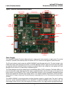
4 latticexp2 standard lattice semiconductor evaluation board user’s guide figure 1. Latticexp2 standard evaluation board power supply the latticexp2 standard evaluation board features a single coaxial input connector to apply power. The coaxial connector is located at the southwest side of the board...
Page 5
5 latticexp2 standard lattice semiconductor evaluation board user’s guide old. Once the 1.2v supply rail is stable, the power manager turns on the 3.3v rail. Once again it waits for the 3.3v supply rail to stabilize before performing any other action. The power manager, having detected both the 1.2v...
Page 6
6 latticexp2 standard lattice semiconductor evaluation board user’s guide note: the board must be un-powered when connecting, disconnecting, or reconnecting the ispdownload® cable or usb cable. Always connect an ispdownload cable’s gnd pin (black wire), before connecting any other jtag pins. Failure...
Page 7
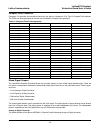
7 latticexp2 standard lattice semiconductor evaluation board user’s guide the jtag port is used for programming the latticexp2 and can also be used for programming the off-chip spi prom. The latticexp2 fpga has several modes it can use to get configuration data. Available sources for config- uration...
Page 8
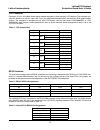
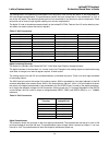
8 latticexp2 standard lattice semiconductor evaluation board user’s guide push-buttons and status leds there are four push-buttons and three leds on the south edge of the evaluation board. Switch sw2 and sw3, the westernmost, are routed to generic latticexp2 i/os. One of these buttons typically acts...
Page 9
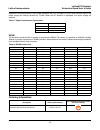
9 latticexp2 standard lattice semiconductor evaluation board user’s guide table 6. Led pin assignments in addition to the discrete chip leds there is a single 7-segment display. Like the discrete leds, a v ol level will cause a segment to illuminate. The segment order is defined in the lumex lds-a30...
Page 10
10 latticexp2 standard lattice semiconductor evaluation board user’s guide figure 3. Oscillator positions the output from the oscillator is routed to two series resistors. One of the series resistors is connected to a primary clock input pin. The other resistor is connected to a pll input pin. It is...
Page 11
11 latticexp2 standard lattice semiconductor evaluation board user’s guide • lcd display, contrast and backlight controls isppac-powr607 the isppac-powr607 is a low-cost power management chip that is used on the latticexp2 standard evaluation board to turn on the dc/dc converters in a controlled seq...
Page 12
12 latticexp2 standard lattice semiconductor evaluation board user’s guide lcd connector connector j13 is a 2x9 100mil center-center header designed to allow the use of lcd displays. The connector pro- vides 5v directly from the dc input (j9). It also has adjustable backlight (r15) and contrast (r16...
Page 13
13 latticexp2 standard lattice semiconductor evaluation board user’s guide compact flash connector connector j14 provides the evaluation board with the ability to interface to 3.3v type ii compact flash devices. The fpga can be programmed to use the various different compact flash protocols. Mixed s...
Page 14
14 latticexp2 standard lattice semiconductor evaluation board user’s guide the analog inputs of the device are connected to four test points. One of these test points is also connected to a 25k ohm discrete potentiometer. The potentiometer permits the input voltage level to vary between 0v to 3.3v a...
Page 15
15 latticexp2 standard lattice semiconductor evaluation board user’s guide operation of the potentiometer is very simple. Whenever the cs is asserted (v il ) and a clock transition occurs, the output voltage will change up/down by 1/128th. When the up direction is requested, the output voltage will ...
Page 16
16 latticexp2 standard lattice semiconductor evaluation board user’s guide technical support assistance hotline: 1-800-lattice (north america) +1-503-268-8001 (outside north america) e-mail: techsupport@latticesemi.Com internet: www.Latticesemi.Com revision history © 2008 lattice semiconductor corp....
Page 17
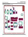
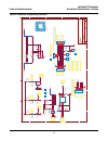
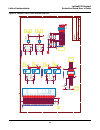
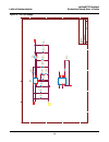
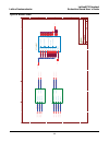
17 latticexp2 standard lattice semiconductor evaluation board user’s guide appendix a. Schematics figure 4. Latticexp2 standard evaluation board 5 5 4 4 3 3 2 2 1 1 d d c c b b a a x p 2b an k 1_10 po t 1 x p 2b an k 1_11 po t 0 x p 2b an k 1_34 po t 2 cl k [0 .. 7 ] cf 8 x p 2 b a n k 0 _ 3 3 cf 1 ...
Page 18
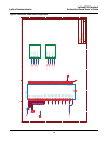
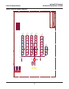
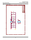
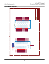
18 latticexp2 standard lattice semiconductor evaluation board user’s guide figure 5. Latticexp2 power and configuration 5 5 4 4 3 3 2 2 1 1 d d c c b b a a x p 2b an k 2 _[ 0. .4 5] x p 2b an k 3 _[ 0. .4 3] x p 2b an k 0_[ 0. .5 1] x p 2b an k 1_[ 0. .3 5] x p 2b an k 5 _[ 0. .5 2] x p 2b an k 4_[ ...
Page 19
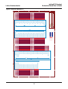
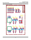
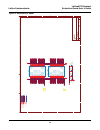
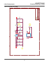
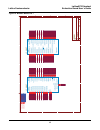
19 latticexp2 standard lattice semiconductor evaluation board user’s guide figure 6. Latticexp2 banks 0 to 3 5 5 4 4 3 3 2 2 1 1 d d c c b b a a x p 2b an k 1 _0 x p 2b an k 1 _1 x p 2b an k 1 _2 x p 2b an k 1 _3 x p 2b an k 1 _4 x p 2b an k 1 _5 x p 2b an k 1 _6 x p 2b an k 1 _7 x p 2b an k 1 _8 x ...
Page 20
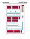
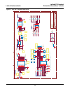
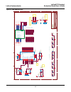
20 latticexp2 standard lattice semiconductor evaluation board user’s guide figure 7. Latticexp2 banks 4 to 7 5 5 4 4 3 3 2 2 1 1 d d c c b b a a x p 2b an k 4 _0 x p 2b an k 4 _1 x p 2b an k 4 _2 x p 2b an k 4 _3 x p 2b an k 4 _4 x p 2b an k 4 _5 x p 2b an k 5 _0 x p 2b an k 5 _1 x p 2b an k 5 _2 x ...
Page 21
21 latticexp2 standard lattice semiconductor evaluation board user’s guide figure 8. Latticexp2 programming interfaces 5 5 4 4 3 3 2 2 1 1 d d c c b b a a xp2 _ j t a g 3 xp2 _ j t a g 2 td o _ c a b l e xp2 _ j t a g 0 xo ba n k 1 _ 2 4 xo ba n k 1 _ 1 7 xo ba n k 1 _ 1 8 xo ba n k 1 _ 2 3 cl9 don_...
Page 22
22 latticexp2 standard lattice semiconductor evaluation board user’s guide figure 9. Latticexp2 bypass capacitors 5 5 4 4 3 3 2 2 1 1 d d c c b b a a xp2 _ bypa s s xp2 _ v c cio [0 ..7 ] vad j ext _ in xp2 _ v c c io 6 +3 _ 3 v +1 _ 2 v vad j +3 _ 3 v xo _ v ccio [0 ..7 ] xp2 _ v c o r e +3 _ 3 v +...
Page 23
23 latticexp2 standard lattice semiconductor evaluation board user’s guide figure 10. Peripherals and clock inputs 5 5 4 4 3 3 2 2 1 1 d d c c b b a a a d _c t r l[ 0. .6 ] da [0 ..5 ] r s 232_[ 0 .. 3] cf [0 ..4 5 ] seg [0 ..7 ] sw it ch [0 ..7 ] lv d s _t [0 .. 3] lv d s _c [0 .. 3] a d _ d [0 ..1...
Page 24
24 latticexp2 standard lattice semiconductor evaluation board user’s guide figure 11. D/a, a/d, 7-segment and rs232 5 5 4 4 3 3 2 2 1 1 d d c c b b a a ad _ c t r l 1 a d _c t r l[ 0. .6 ] ad _ c t r l 0 ad _ c t r l 2 ad _ c t r l 3 ad _ c t r l 4 ai n 0 a d _ d [0 ..1 1 ] ad _ c t r l 5 ai n 1 ad ...
Page 25
25 latticexp2 standard lattice semiconductor evaluation board user’s guide figure 12. Compact flash, lvds, switches and lcd 5 5 4 4 3 3 2 2 1 1 d d c c b b a a cf 0 cf 1 cf 2 cf 3 cf 4 cf 5 cf 6 cf 7 cf 8 cf 9 cf 1 0 cf 1 1 cf 1 2 cf 1 3 cf 1 4 cf 1 5 cf 1 6 cf 1 7 cf 1 8 cf 1 9 cf 2 0 cf 2 1 cf [0 ...
Page 26
26 latticexp2 standard lattice semiconductor evaluation board user’s guide figure 13. Asynchronous sram 5 5 4 4 3 3 2 2 1 1 d d c c b b a a sr a m _ a 1 7 sr a m _ a 1 6 sr a m _ a 1 5 sr a m _ o e sr a m _ b e1 sr a m _ b e0 sr a m _ d 1 5 sr a m _ d 1 4 sr a m _ d 1 3 sr a m _ d 1 2 sr a m _ d 1 1...
Page 27
27 latticexp2 standard lattice semiconductor evaluation board user’s guide figure 14. Prototype grid 5 5 4 4 3 3 2 2 1 1 d d c c b b a a x p 2b an k 6 _6 xp2 _ io _ 0 x p 2b an k 6 _12 xp2 _ io _ 2 x p 2b an k 6 _17 xp2 _ io _ 5 x p 2b an k 6 _38 xp2 _ io _ 7 x p 2b an k 6 _39 xp2 _ io _ 8 x p 2b an...
Page 28
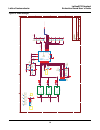
28 latticexp2 standard lattice semiconductor evaluation board user’s guide figure 15. Power manager 5 5 4 4 3 3 2 2 1 1 d d c c b b a a vi n e n _1_2v e n _3_3v en _ v a d j e n _1_2v e n _3_3v en _ v a d j bia s vi n vp ac pa c _ pw r d n _ n pa c _ t c k pa c _ t d i pa c _ t d o vp ac x p 2b an k...
Page 29
29 latticexp2 standard lattice semiconductor evaluation board user’s guide figure 16. 1.2v core supply 5 5 4 4 3 3 2 2 1 1 d d c c b b a a s s _1_2 f b _1_2 e n _1_2 b s _1_2 c o m p _1_2 vi n s w _1_2 r c _1_2 +1 _ 2 v vi n 1_2_a d j 1 1_2_a d j 2 e n _1_2 vi n + 1_2v e n _1_2v ti tl e siz e d o c ...
Page 30
30 latticexp2 standard lattice semiconductor evaluation board user’s guide figure 17. 3.3v power converter 5 5 4 4 3 3 2 2 1 1 d d c c b b a a e n _3_3 f b _3_3 s s _3_3 bs_ 3 _ 3 c o m p _3_3 s w _3_3 vi n rc_ 3 _ 3 + 3_3v vi n e n _3_3 vi n +3 _ 3 v e n _3_3v ti tl e siz e d o c u m e n t n u m b ...
Page 31
31 latticexp2 standard lattice semiconductor evaluation board user’s guide figure 18. Adjustable power supply 5 5 4 4 3 3 2 2 1 1 d d c c b b a a en _ v a d j fb _ a d j ss_ a d j ad j _ 1 _ 2 bs_ a d j rc_ a dj co m p _ a dj vad j vi n sw _ a d j vad j vi n vad j _ 1 vad j _ 2 en _ v a d j vi n vad...
Page 32
32 latticexp2 standard lattice semiconductor evaluation board user’s guide figure 19. Usb download phy 5 5 4 4 3 3 2 2 1 1 d d c c b b a a us b - us b + cl k _ e n us b 7 us b 6 us b 5 us b 4 us b 3 us b 2 us b 1 us b 0 us b 2 3 us b 2 2 us b 2 1 us b 2 0 us b 1 9 us b 1 8 us b 1 7 us b 1 6 us b 1 5...
Page 33
33 latticexp2 standard lattice semiconductor evaluation board user’s guide figure 20. Machxo power 5 5 4 4 3 3 2 2 1 1 d d c c b b a a xo ba n k 0 _ [0 ..2 3 ] xo ba n k 1 _ [0 ..2 8 ] x o b a n k 01_[ 0. .1 ] x o b a n k 2_[ 0 .. 25] x o b a n k 3_[ 0 .. 28] xo ba n k 4 _ [0 ..2 7 ] xo ba n k 5 _ [...
Page 34
34 latticexp2 standard lattice semiconductor evaluation board user’s guide figure 21. Machxo banks 0 to 3 5 5 4 4 3 3 2 2 1 1 d d c c b b a a xo ba n k 0 _ 0 xo ba n k 0 _ 1 xo ba n k 0 _ 2 xo ba n k 0 _ 3 xo ba n k 0 _ 4 xo ba n k 0 _ 5 xo ba n k 0 _ 6 xo ba n k 0 _ 7 xo ba n k 0 _ 8 xo ba n k 0 _ ...
Page 35
35 latticexp2 standard lattice semiconductor evaluation board user’s guide figure 22. Machxo banks 4 to 7 5 5 4 4 3 3 2 2 1 1 d d c c b b a a xo ba n k 5 _ 0 xo ba n k 5 _ 1 xo ba n k 5 _ 2 xo ba n k 5 _ 3 xo ba n k 5 _ 4 xo ba n k 5 _ 5 xo ba n k 5 _ 6 xo ba n k 5 _ 7 xo ba n k 5 _ 8 xo ba n k 5 _ ...
Page 36
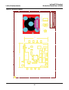
36 latticexp2 standard lattice semiconductor evaluation board user’s guide figure 23. Placement proposal 5 5 4 4 3 3 2 2 1 1 d d c c b b a a ti tl e siz e d o c u m e n t n u m b e r r e v d a te : s h eet of 000 p lac em en t p rop os al l a tt ic e s e m ic o n d u c to r co rp o ra ti o n 5555 n ...


