- DL manuals
- Magnavox
- TV VCR Combo
- 27MDTR10S
- Service Manual
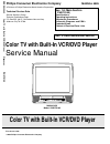
Magnavox 27MDTR10S Service Manual
Color TV with Built-In VCR/DVD Player
First Issue: 10/02
2002 Philips Consumer Electronics Company
Philips Consumer Electronics Company
A Division of Philips Electronics North America Corporation
Technical Service Data
Service Solutions Group
Technical Publications Dept.
P.O. Box 555, 401 E. Old Andrew Johnson Hwy.
Jefferson City,TN 37760
MANUAL 5885
Sec. 1A: Main Section
( 27MDTR10S )
Specifications
Operating Instructions
Adjustment Procedures
Schematic Diagrams and CBA’s
Exploded Views
Cabinet & Electrical Parts Lists
MAGNAVOX
Model: 27MDTR10S
Sec. 2: Deck Mechanism Section
MANU
AL 5
885
Color
TV w
it
h
Buil
t-
In V
CR/D
V
D Pl
a
yer
Magna
v
o
x
27
MDTR1
0
S
Color TV with Built-In VCR/DVD Player
Service Manual
Summary of 27MDTR10S
Page 1
Color tv with built-in vcr/dvd player first issue: 10/02 2002 philips consumer electronics company philips consumer electronics company a division of philips electronics north america corporation technical service data service solutions group technical publications dept. P.O. Box 555, 401 e. Old an...
Page 2
Philips consumer electronics company a division of philips electronics north america corporation technical service data service solutions group technical publications dept. P.O. Box 555, 401 e. Old andrew johnson hwy. Jefferson city,tn 37760 manual 5885 sec. 1a: main section ( 27mdtr10s ) specificat...
Page 3: Important Safety Notice
Important safety notice proper service and repair is important to the safe, reliable operation of all philips consumer electronics company** equipment. The service procedures recommended by philips and described in this service manual are effective methods of performing service operations. Some of t...
Page 4: Table of Contents
Table of contents [ main section ] page specifications . . . . . . . . . . . . . . . . . . . . . . . . . . . . . . . . . . . . . . . . . . . . . . . . . . . . . . . . . . . . . . . . . . . . . . . . . . . . 1-1-1 laser beam safety precautions . . . . . . . . . . . . . . . . . . . . . . . . . . . . ....
Page 5: Specifications
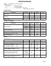
1-1-1 t601sp specifications *ˆ mode---------sp mode unless otherwise specified * test input terminal -------------video input (1vp-p) audio input (-10db) -----------------------ant. Input (80db µv) video: 87.5% audio: 25khz dev (1khz sin) measurement at tp description condition unit nominal limit 1....
Page 6
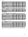
1-1-2 t601sp all items are measured across 8 Ω resistor at speaker output terminal. * all items are measured at tp1701 and tp1702. Note: nominal specifications represent the design specifications. All units should be able to approximate these. Some will exceed and some may drop slightly below these ...
Page 7
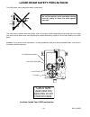
1-2-1 dvd_laser drive mecha assembly laser beam radiation laser pickup turntable laser radiation when open. Do not stare into beam. Caution laser beam safety precautions this dvd player uses a pickup that emits a laser beam. The laser beam is emitted from the location shown in the figure. When check...
Page 8: Important Safety Precautions
1-3-1 dvd_sfn1 important safety precautions product safety notice some electrical and mechanical parts have special safety-related characteristics which are often not evi- dent from visual inspection, nor can the protection they give necessarily be obtained by replacing them with components rated fo...
Page 9
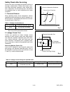
1-3-2 dvd_sfn1 chassis or secondary conductor d d' primary circuit terminals ac voltmeter (high impedance) exposed accessible part b earth ground power cord plug prongs z 1.5k 0.15 f safety check after servicing examine the area surrounding the repaired location for damage or deterioration. Observe ...
Page 10: Standard Notes For Servicing
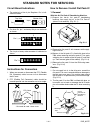
1-4-1 dvd_note standard notes for servicing circuit board indications a. The output pin of the 3 pin regulator ics is indi- cated as shown. B. For other ics, pin 1 and every fifth pin are indicated as shown. C. The 1st pin of every male connector is indicated as shown. Instructions for connectors 1....
Page 11
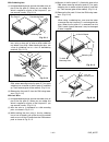
1-4-2 dvd_note with soldering iron: (1) using desoldering braid, remove the solder from all pins of the flat pack-ic. When you use solder flux which is applied to all pins of the flat pack-ic, you can remove it easily. (fig. S-1-3) (2) lift each lead of the flat pack-ic upward one by one, using a sh...
Page 12
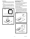
1-4-3 dvd_note 2. Installation (1) using desoldering braid, remove the solder from the foil of each pin of the flat pack-ic on the cba so you can install a replacement flat pack-ic more easily. (2) the “i” mark on the flat pack-ic indicates pin 1. (see fig. S-1-7.) be sure this mark matches the 1 on...
Page 13: Preparation For Servicing
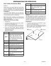
1-5-1 td603pfs preparation for servicing how to enter the service mode caution: 1 optical sensors are used for tape start and end sen- sor on this equipment. Read this page carefully and prepare as described on this page before starting to service; otherwise, the unit may operate unexpectedly. Prepa...
Page 14
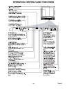
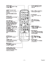
1-6-1 td603ib operating controls and functions.
Page 15
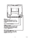
1-6-2 td603ib.
Page 16: Remote Control Operation
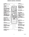
1-7-1 td603ibr remote control operation.
Page 17
1-7-2 td603ibr.
Page 18
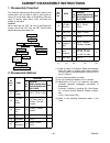
1-8-1 td603dc cabinet disassembly instructions 1. Disassembly flowchart this flowchart indicates the disassembly steps for the cabinet parts and the cba in order to gain access to item(s) to be serviced. When reassembling, follow the steps in reverse order. Bend, route and dress the cables as they w...
Page 19
1-8-2 td603dc reference notes in the table caution ! When removing the crt, be sure to discharge the anode lead of the crt with the crt ground wire before removing the anode cap. Reference notes in the table caution 1: discharge the anode lead of the crt with the crt ground wire before removing the ...
Page 20
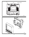
1-8-3 td603dc fig. 1 s-1 s-1 s-1 s-3 s-2 [1] rear cabinet s-1 s-1 s-2 s-3 s-1 s-1 s-1 s-1 [1] rear cabinet s-1 fig. 2.
Page 21
1-8-4 td603dc fig. 3 s-5 s-5 [5] shield box [3] tray chassis [2] h.V. Cba (wih holder) h.V. Cba [6] dvd mechanism [11] deck assembly [12] main cba [8] filter cba [9] bottom plate [10] power supply/ av cba s-6 s-8 s-9 s-9 s-8 s-8 s-10 s-10 s-11 s-11 s-12 s-10
Page 22
1-8-5 td603dc s-4 s-4 s-4 s-4 [4] crt anode cap crt cba fig. 4 fig. 5 cn101 dvd mechanism [7] dvd main cba unit cn401 s-7 s-7 view for b pickup unit c b three short lands view for c slide view for a type a type b three short lands a.
Page 23
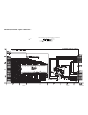
1-8-6 td603dc fig. 6 cn501 screen focus cl504a cl501 crt cba cn501 cn101 cn401 cn701 factory use only dvd main cba cn571 cl502a cl503a cl501a h.V. Cba cn403 cn402 cn404 cn401 filter cba to power supply/ av cba speaker cn2401 cn2402 cn2601 cn2801 cn2802 cn2803 cn2804 cn2602 anode crt gnd tuner main c...
Page 24
1-9-1 td603ea electrical adjustment instructions general note: "cba" is abbreviation for "circuit board assembly." note: electrical adjustments are required after replacing circuit components and certain mechanical parts. It is important to perform these adjustments only after all repairs and replac...
Page 25
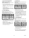
1-9-2 td603ea 2. Auto aft (vco) adjustment purpose: to operate aft correctly. Symptom of misadjustment: aft does not work cor- rectly and/or synchronization is faulty. 1. Set the unit to the video mode with no signal input. 2. Enter the service mode. (see page 1-9-1.) then press number "3" button on...
Page 26
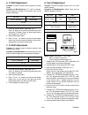
1-9-3 td603ea 6. V. Shift adjustment purpose: to obtain correct vertical position of screen image. Symptom of misadjustment: if v. Shift is incorrect, vertical position of image on the screen may not be properly displayed. 1. Enter the service mode. (see page 1-9-1.) press "9" button on the service ...
Page 27
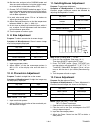
1-9-4 td603ea 10.Set the color analyzer to the chroma mode and after zero point calibration, bring the optical recep- tor to the center on the tube surface (crt). 11.Choose cut off/drive mode then press "4" but- ton on the service remote control unit for red adjust- ment. Press "5" button on the ser...
Page 28
1-9-5 td603ea 13. Sif adjustment purpose: to set the sif (sound intermediate fre- quency). Symptom of misadjustment: audio may not sound correctly. Note: this adjustment automatically done by the chrominance ic (ic1301). 14. Ccs text box location when replacing the crt, the ccs text box might not st...
Page 29
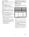
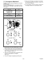
1-9-6 td603ea 17. Convergence adjustment purpose: to obtain proper convergence of red, green and blue beams. Symptom of misadjustment: if convergence adjust- ment is incorrect, the edge of white letters may have color edges. 1. Set the unit to the aux mode which is located before ch2 then input a do...
Page 30
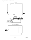
1-9-7 td603ea tp1001 main cba power supply/av cba h.V. Cba agc vr2601 +b adj r583 h adj j520 x-ray j522 x-ray h.Size vr530 vr531 j523 +b upper focus vr lower screen vr h. Pincushion adjustment points and test points.
Page 31: Firmware Renewal Mode
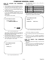
1-10-1 td603rom firmware renewal mode how to update the firmware version 1. Turn the power on and remove the disc on the tray. 2. To enter the dvd mode, press [select] button on the remote control unit. (dvd indicator lights on.) 3. To open the tray, press [open/close] button on the remote control u...
Page 32
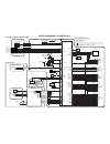
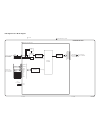
Control head cl1402 ac head assembly main cba power supply / av cba rf-sw t-reel dv-sync c-sync c-sync v-env ctl(+) d1224 s-led d1204 rec d1216 dvd d1217 tv/vcr q1210 q1211 q1207 p-on+5v rec-led key0 rs1201 remote sensor key1 kye2 dvd-h tv/vcr-led reset rota d-rec-h d-rec-h rec-safety a-mute-h scl r...
Page 33
Video block diagram 1-11-3 1-11-4 td603blv rec video signal pb video signal mode: sp/rec luminance signal process main cba cl1401 q1401 tp1402 v-out v-agc r p fbc y/c mix ccd 1h delay r p doc ynr y/c comb chrominance signal process ic1401 video/audio signal process 35 42 38 chara mix 6db amp vxo env...
Page 34
Audio block diagram block diagram for section 2 (deck mechanism) main cba power supply / av cba pb-audio signal dvd audio signal data(audio) signal rec-audio signal 1-11-5 ic1401 mode : sp/rec td603bla 1-11-6 bias osc q1872 p-on+5v p-on+5v q1871 q1873 q1874 q1875 (audio process) n-a-in n-a-out tp180...
Page 35
57 48 47 13 14 69 6 7 r-ch insel l-ch insel nor sw serial data decoder output select vco lpf l-ch bpf r-ch pnr pilot det noise det stereo pll stereo filter sap filter sif demod sap demod l-r demod st/sap sw matrix l-ch pnr lim dev comp sw noise vco lpf lim dev comp comp dc sw noise dbx dec env det m...
Page 36
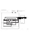
Td603blc 1-11-9 1-11-10 x1301 3.58mhz cn1301 cn1803 cn1302 4.5mhz trap cf1302 4.5mhz bpf cf1301 saw filter sf1001 ic1301(video/audio/chroma/deflection/if) tu1001 if agc tp2201 dvd-v sda scl fsc 1 11 5 4 8 ic1201 (system control/osd) v-sync h-sync osd-r osd-g osd-b 59 58 60 62 63 64 osd-blk sif yca-v...
Page 37
Pulse up amp thermal protection 3 6 7 1 5 v-drive 7 h-drive 3 8 10 7 9 6 green amp blue amp q503 q502 q501 h.Drive q591 q571 t572 td603blcrt fbp-in acl/abl crt/h.V. Block diagram v- drive h- drive d.Y. L551 ic551 (v-deflection control) t571 f.B.T. Anode focus screen 2 4 cl503a 6 h.V. Cba crt cba cl5...
Page 38
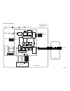
Power supply block diagram 6 4 2 1 14 11 9 8 10 line filter bridge rectifier t2601 ic2611 error voltage det w2601 f2601 4a/125v l2601 d2603 d2606 td603blp degaussing coil cn2601 ps2601 hot cold 1-11-14 1-11-13 power supply/av cba main cba filter cba dvd main cba unit note : the voltage for parts in ...
Page 39
Dvd system control block diagram td603blds 1-11-15 1-11-16 59 60 49 82 ic301 (front end processor) ic601 (dvd host processor) osci osco 23 24 (16.9344mhz) x301 clock x601 27mhz 120 ready 48 hang /fers trev tfwd tin tout ready /fers tin tout 10 sen 46 mute 47 ps 64 from/to dvd signal process block di...
Page 40
Tout tin trev tfwd ps rf signal process/servo block diagram td603blrf 1-11-17 1-11-18 a 6 b 9 c 10 d 7 f 4 e 5 dvd-ld 12 cd-ld 20 pd-moni 11 gnd 14 gnd 13 gnd 19 fs(+) 17 fs(-) 16 ts(+) 15 ts(-) 18 cn101 cn101 cn101 lm(+) 1 lm(-) 2 sp(-) 6 sp(+) 7 sl(+) 9 sl(-) 8 cn401 ic401 ic103 (servo drive) (sw)...
Page 41
Dvd signal process block diagram td603bld 1-11-19 1-11-20 ic201 (dvd signal process) para0 para0-para7 para1 para2 para3 para4 para5 para6 para7 from/to rf signal process/servo block diagram 111 110 arf narf testsg data slicer pll vco cpu interface video/audio interface dvd demodulator memory manage...
Page 42
Dvd video block diagram td603bldv 1-11-21 1-11-22 cn701 5 14 dvd-y 9 10 dvd-c filter cba data(video) signal dvd video signal data(audio) signal ic601 (dvd host processor) ic604 ic602 (8mbit flash memory) para0 para7 a0 a18 data0 a d 0 a d 13 data15 dq0 dq15 ce oe we cs3 oe dqm0 a d 0 a d 13 ~ d q 0 ...
Page 43
Dvd audio block diagram td603blda 1-11-23 1-11-24 ic801 (audio dac) 7 8 12 11 cn701 cn404 13 6 dvd audio(l) 15 4 dvd audio(r) 12 7 a-mute(l) 14 5 a-mute(r) 16 3 a-mute 1 2 3 13 14 15 16 from dvd video block diagram serial port serial control 4x/8x oversampling digital filter /function controller enp...
Page 44
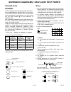
1-12-1 sc_5 (top view) (bottom view) (bottom view) electrolytic capacitor + transistor or digital transistor npn transistor pnp transistor npn digital transistor pnp digital transistor (top view) (top view) e c b e c b e c b (top view) (top view) e c b e c b 2 3 1 5.0 (2.5) play mode rec mode 5.0 th...
Page 45
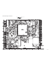
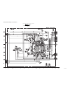
1-12-2 main 1/4 schematic diagram parts location guide ref no. Position ref no. Position ref no. Position ref no. Position ref no. Position c1203 b-4 c1635 b-1 ic1602 b-2 r1226 a-4 r1293 e-4 c1204 b-4 c1636 c-1 r1227 b-4 r1294 e-3 c1205 b-4 l1201 d-2 r1228 b-3 r1295 e-4 c1207 a-4 cl1201 a-3 l1202 f-...
Page 46
1-12-3 1-12-4 1-12-5 td603scm1 main 1/4 schematic diagram voltage indications on the schematic diagrams are as shown below: the same voltage for both play, rec & dvd modes. Indicates that the voltage is not consistent here. Play mode rec mode 1 2 3 5.0 5.0 (2.5) [0.5] ~ dvd mode.
Page 47
1-12-6 1-12-7 1-12-8 td603scm2 main 2/4 schematic diagram voltage indications on the schematic diagrams are as shown below: the same voltage for both play, rec & dvd modes. Indicates that the voltage is not consistent here. Play mode rec mode 1 2 3 5.0 5.0 (2.5) [0.5] ~ dvd mode.
Page 48
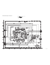
1-12-9 main 2/4 schematic diagram parts location guide ref no. Position ref no. Position ref no. Position ref no. Position c1403 j-2 c1507 m-3 l1404 i-4 r1435 i-3 c1410 k-2 c1508 n-3 l1405 l-5 r1495 l-2 c1411 k-2 c1509 m-3 l1501 m-2 r1496 l-1 c1412 k-2 c1510 n-3 l1502 m-3 r1497 l-2 c1413 k-2 c1511 n...
Page 49
Main 3/4 schematic diagram parts location guide 1-12-10 ref no. Position ref no. Position ref no. Position c1005 q-3 d1301 s-1 r1313 t-2 c1006 p-3 d1302 s-1 r1314 t-2 c1007 p-3 d1303 s-2 r1315 t-2 c1301 r-2 d1304 t-2 r1316 t-3 c1302 r-2 d1305 t-2 r1318 t-3 c1303 r-2 d1306 u-2 r1319 t-3 c1305 s-2 d13...
Page 50
1-12-11 1-12-12 1-12-13 td603scm3 main 3/4 schematic diagram voltage indications on the schematic diagrams are as shown below: the same voltage for both play, rec & dvd modes. Indicates that the voltage is not consistent here. Play mode rec mode 1 2 3 5.0 5.0 (2.5) [0.5] ~ dvd mode.
Page 51
1-12-14 1-12-15 1-12-16 td603scm4 main 4/4 schematic diagram voltage indications on the schematic diagrams are as shown below: the same voltage for both play, rec & dvd modes. Indicates that the voltage is not consistent here. Play mode rec mode 1 2 3 5.0 5.0 (2.5) [0.5] ~ dvd mode.
Page 52
Main 4/4 schematic diagram parts location guide ref no. Position ref no. Position ref no. Position c1601 aa-3 c1778 x-4 r1605 z-2 c1602 aa-3 c1779 x-4 r1606 aa-2 c1603 z-3 c1780 x-4 r1607 aa-2 c1604 aa-3 c1781 x-4 r1608 aa-2 c1605 bb-3 c1782 w-4 r1609 bb-3 c1606 z-2 c1783 w-4 r1610 aa-2 c1608 aa-3 c...
Page 53
Ref no. Position ref no. Position ref no. Position ref no. Position ref no. Position ref no. Position ref no. Position ref no. Position c1005 f-5 c1318 e-4 c1451 c-5 c1766 d-2 cn1303 f-4 d1806 a-5 q1603 f-2 r1248 b-4 c1006 f-5 c1319 f-4 c1452 c-2 c1767 d-2 cn1802 b-5 d1807 a-5 q1608 f-2 r1249 b-4 c1...
Page 54
Rf-sw tp1401 wf1 env tp1403 wf6 gnd tp1632 ctl-amp-out tp1201 wf3 d1304 (c-trap adjustment) v-out tp1402 wf5 na-in -yca tp1802 wf7 agc tp1001 cathode 1-12-21 1-12-22 1-12-23 btd500f01013 sensor cba top view (start-sensor) bhb300f01013a bhb300f01013b sensor cba top view (end-sensor) bhb300f01013a bhb...
Page 55
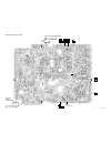
Pin 7 of ic1401 wf2 pin 61 of ic1401 wf4 pin 42 of ic1401 wf17 pin 59 of ic1201 wf16 pin 58 of ic1201 wf10 wf8 pin 11 of ic1301 pin 20 of ic1301 wf9 1-12-24 1-12-25 1-12-26 btd500f01013 main cba bottom view.
Page 56
Crt schematic diagram td603sccrt 1-12-27 1-12-28 voltage indications on the schematic diagrams are as shown below: the same voltage for both play, rec & dvd modes. Indicates that the voltage is not consistent here. Play mode rec mode 1 2 3 5.0 5.0 (2.5) [0.5] ~ dvd mode crt schematic diagram parts l...
Page 57
Q503 collector wf13 q502 collector wf14 q501 collector wf15 crt cba top view 1-12-29 1-12-30 btd370f01043-b crt cba bottom view crt cba parts location guide ref no. Position c503 b-1 c506 b-1 c508 b-1 c510 b-2 c511 a-1 c512 a-1 cl501 a-1 cl504a b-1 cn501 a-2 d500 b-1 d501 b-1 d502 b-2 q501 a-1 q502 ...
Page 58
H.V. Schematic diagram 1-12-31 1-12-32 td603schv voltage indications on the schematic diagrams are as shown below: the same voltage for both play, rec & dvd modes. Indicates that the voltage is not consistent here. Play mode rec mode 1 2 3 5.0 5.0 (2.5) [0.5] ~ dvd mode.
Page 59
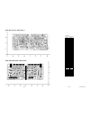
C579 note : red letters indicate additional parts on the component side. +b j523 r583 (h adjustment) x’ ray j520, j522 gnd j516 h.V. Cba top view 1-12-33 1-12-34 btd370f01043-a h.V. Cba parts location guide ref no. Position ref no. Position ref no. Position ref no. Position c531 b-2 c573 a-1 cl503a ...
Page 60
Pin 5 of cn571 wf12 q571 collector wf11 1-12-35 1-12-36 btd370f01043-a h.V. Cba bottom view.
Page 61
Junction-a cba top view btd370f01043-d junction-a cba bottom view junction-b cba top view junction-b cba bottom view btd370f01043-c 1-12-37 1-12-38 ref no. Position ref no. Position ref no. Position ref no. Position ref no. Position c2209 e-2 c2631 a-2 d2626 e-5 q2601 b-5 r2301 b-3 c2211 e-2 c2632 e...
Page 62
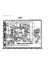
Power supply/av schematic diagram 1-12-39 1-12-40 1-12-41 td603scp caution ! Fixed voltage power supply circuit is used in this unit. If main fuse (f2601) is blown, check to see that all components in the power supply circuit are not defective before you connect the ac plug to the ac power supply. O...
Page 63
+b adj vr2601 1-12-42 1-12-43 1-12-44 btd500f01023a power supply / av cba top view caution ! Fixed voltage power supply circuit is used in this unit. If main fuse (f2601) is blown, check to see that all components in the power supply circuit are not defective before you connect the ac plug to the ac...
Page 64
Wf18 pin 14 of cn2402 wf19 pin 16 of cn2402 wf20 pin 18 of cn2402 wf23 pin 11 of cn2402 wf22 pin 7 of cn2402 wf21 pin 5 of cn2402 caution ! Fixed voltage power supply circuit is used in this unit. If main fuse (f2601) is blown, check to see that all components in the power supply circuit are not def...
Page 65
1-12-48 1-12-49 1-12-50 td603scd1 dvd main 1/4 schematic diagram “ “ = smd voltage indications on the schematic diagrams are as shown below: the same voltage for both play & stop modes. Indicates that the voltage is not consistent here. Play mode stop mode 1 2 3 5.0 5.0 (2.5) ~.
Page 66
Dvd main 2/4 schematic diagram 1-12-51 1-12-52 1-12-53 td603scd2 “ “ = smd voltage indications on the schematic diagrams are as shown below: the same voltage for both play & stop modes. Indicates that the voltage is not consistent here. Play mode stop mode 1 2 3 5.0 5.0 (2.5) ~.
Page 67
Dvd main 3/4 schematic diagram 1-12-54 1-12-55 1-12-56 td603scd3 “ “ = smd voltage indications on the schematic diagrams are as shown below: the same voltage for both play & stop modes. Indicates that the voltage is not consistent here. Play mode stop mode 1 2 3 5.0 5.0 (2.5) ~.
Page 68
Dvd main 4/4 schematic diagram td603scd4 1-12-57 1-12-58 “ “ = smd voltage indications on the schematic diagrams are as shown below: the same voltage for both play & stop modes. Indicates that the voltage is not consistent here. Play mode stop mode 1 2 3 5.0 5.0 (2.5) ~.
Page 69
Filter schematic diagram td603scf 1-12-59 1-12-60 filter schematic diagram parts location guide ref no. Position c406 b-4 c407 b-2 c416 b-2 c417 b-2 c418 b-4 cn401 c-4 cn402 c-2 cn403 a-4 cn404 a-2 d401 b-4 d402 b-1 d403 b-2 d404 b-2 l401 b-3 l404 b-4 l406 b-4 l407 c-4 l408 b-4 l409 b-4 l410 c-4 l41...
Page 70
Filter cba top view filter cba bottom view btd500f01023b 1-12-61 1-12-62 filter cba parts location guide ref no. Position c406 c-2 c407 b-2 c416 b-1 c417 b-1 c418 d-1 cn401 c-2 cn402 a-2 cn403 c-1 cn404 b-1 d401 d-1 d402 a-2 d403 a-2 d404 b-2 l401 c-2 l404 c-2 l406 c-1 l407 d-1 l408 d-2 l409 d-1 l41...
Page 71
Td603twf 1-13-1 1-13-2 waveforms wf2 main 2/4 schematic diagram ic1401 pin 61 wf1 main 2/4 schematic diagram tp1401 rf-sw upper: wf6 lower: wf1 main 2/4 schematic diagram tp1403 env wf5 main 2/4 schematic diagram tp1402 v-out wf4 main 2/4 schematic diagram ic1401 pin 42 wf8 main 2/4 schematic diagra...
Page 72
1-13-4 td603dwf 1-13-3 note: input cd: 1khz play (wf21~wf23) dvd: power on (stop) mode (wf18~wf20) waveforms wf23 spdif pin 11 of cn2402 1v 0.2usec wf18 pin 14 of cn2402 wf20 pin 18 of cn2402 wf21 dvd-audio(l) pin 5 of cn2402 1v 0.5msec wf22 dvd-audio(r) pin 7 of cn2402 1v 0.5msec wf19 pin 16 of cn2...
Page 73
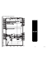
Wiring diagram 1-14-1 td603wit 1-14-2 1 2 3 heater crt cba btd370f01043-b h.V. Cba btd370f01043-a focus screen gnd l551 d.Y. Hd vd cl501a cn1302 cl503a main cba (btd500f01013) power supply & av cba (btd500f01023-a) h e at e r g n d 3 2 1 c l5 01 b cn1301 cn501 w2601 t571 fbt crt red green blue gnd 4...
Page 74
Dvd mecha 1-14-3 1-14-4 wiring diagram dvd main cba unit td603wid pick up unit fg cba cn101 cn401 fg sensor 1 lm (+ ) 2 lm (- ) 3 t r ay -i n 4 t r ay -o u t 5 g n d 6 s p (- ) 7 s p (+ ) 8 s l( -) 9 s l( +) 10 f g -i n 11 p -o n +3 .3 v (d ) 1 g n d 2 v r e f 3 p -o n +5 v 4 f 5 e 6 a 7 d 8 n u 9 b...
Page 75
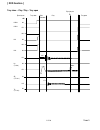
1-15-1 td603ti system control timing charts [ vcr section ] mode sw : ld-sw ld-sw position detection a/d input voltage limit (calculated voltage) symbol 3.76v~4.50v (4.12v) ej 4.51v~5.00v (5.00v) cl 0.00v~0.25v (0.00v) sb 1.06v~1.50v (1.21v) tl 0.66v~1.05v (0.91v) fb 1.99v~2.60v (2.17v) sf 1.51v~1.9...
Page 76
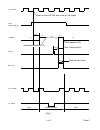
1-15-2 td603ti 18 rf-sw f-ad (internal signal) c-drive pb ctl 66 c-f/r 16 h-a-sw 15 rota at "h" "z" "h" "l" "l" st bl still frame advance still the first rise of rf-sw after a rise in f-ad signal stop detection (t2) slow tracking value acceleration detection (t1) reversal limit value fig. 1.
Page 77
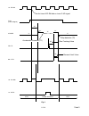
1-15-3 td603ti "h" "z" "h" "l" "l" 18 rf-sw f-ad (internal signal) c-drive pb ctl 66 c-f/r 16 h-a-sw 15 rota still still at st bl stop detection (t2) acceleration detection (t1) slow tracking value reversal limit value frame advance the first rise of rf-sw after a rise in f-ad signal fig. 2.
Page 78
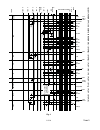
1-15-4 td603ti 1. Eject (po w er off) -> cassette in (po w er on) -> st op(b) -> st op(a) -> pla y -> rs -> fs -> pla y -> still -> pla y -> st op(a) eject cass.Load st-s,/ end-s "off" play rew ff play play stop /eject 0.2s 0.7s 0.2s 0.2s ld-fwd stop(a) stop(a) ld-fwd ld-rev 0.4s 0.2s ld-fwd ld-fwd ...
Page 79
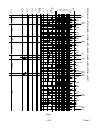
1-15-5 td603ti st-s,/ end-s "on" rec rew ff stop /eject 1.0s 0.5s 0.2s 0.5s 0.2s 0.5s 0.5s 0.5s 0.2s 0.2s 0.2s 1.5s 2.5s short rev 1.0s 0.2s ld-fwd ld-fwd stop(a) stop(a) stop(a) cass. Unld eject stop(a) ld-rev ld-rev ld-rev ld-rev ld-fwd ld-fwd ld-fwd ld-fwd ld-fwd ld-fwd ld-fwd rec pause rec rec r...
Page 80
1-15-6 td603ti lsw2 lsw1 lm- lm+ i/o (tl123) sp ( tp122 ) tv ( tl122 ) 0v +5v 0v tray close tray open tray close ~ play / play ~ tray open play 0v eject key on +6v +2v +5v 0v disc rotation eject key on +2v 2.0s 0v +6v 4.4s 1.2s 700ms 1.7s 0v [ dvd section ].
Page 81
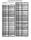
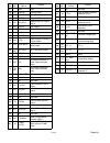
1-16-1 td603pin ic pin function descriptions ic1201 ( servo / system control/tv/ osd/timer ic ) “h” ≥ 4.5v, “l” ≤ 1.0v pin no. In/ out signal name function 1 in ld-sw loading switch input 2 in p-safety 1 power supply failure detection 1 3 in p-safety 2 power supply failure detection 2 4 in st/sap-in...
Page 82
1-16-2 td603pin 57 - gnd gnd 58 in h-sync h-sync input 59 in v-sync v-sync input 60 out osd-blk output for picture cut off 61 out dg-on-h degaussing coil control signal 62 out osd-b blue output 63 out osd-g green output 64 out osd-r red output 65 out a-mute-h audio mute output 66 out c-f/r capstan m...
Page 83: Lead Identifications
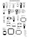
1-17-1 td603le 2sc1627y-tpe2 2sa950(y,o) kta1271(y) 2sc2482 tpe6 2sc3468(e,d)-ae 2sc3400 2sa1175(e,f) kta1267(gr) krc103m bn1f4m-t ktc3199(gr) 2sc2785(j,h,f) 2sa1015-gr(tpe2) ba1f4m-t 2sc2236-y-tpe6,c kra103m kta1266(gr) e c b e c b 2sc1815-gr(tpe2) 2sc3331(t,u) 2sc2120-(o,y)(tpe2) 2sa1318(t,u)-aanp...
Page 84: Electrical Parts List
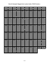
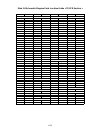
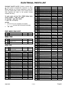
20021002 1-18-1 td603el electrical parts list product safety note: products marked with a # have special characteristics important to safety. Before replacing any of these components, read care- fully the product safety notice in this service manual. Don't degrade the safety of the product through i...
Page 85
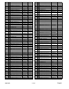
20021002 1-18-2 td603el electrolytic cap. 1µf/50v ±20% ce1jmastl1r0 4835 124 47014 c1320 electrolytic cap. 100µf/16v ±20% or ce1cmasdl101 4835 124 47033 electrolytic cap. 100µf/16v ±20% ce1cmastl101 4835 124 47033 c1322 electrolytic cap. 1µf/50v ±20% or ce1jmasdl1r0 4835 124 47305 electrolytic cap. ...
Page 86
20021002 1-18-3 td603el c1636 ceramic cap.(ax) 0.1µf/50v +80/-20% (f) cca1jztfz104 4835 122 47731 c1701 electrolytic cap. 47µf/25v ±20% or ce1emasdl470 4835 124 47102 electrolytic cap. 47µf/25v ±20% ce1emastl470 4835 124 47102 c1722 electrolytic cap. 1µf/50v ±20% or ce1jmasdl1r0 4835 124 47305 elect...
Page 87
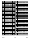
20021002 1-18-4 td603el zener diode dz-6.2bsbt265 ndtb0dz6r2bs 4835 130 38039 d1203 zener diode mtzjt-776.2b or qdtb0mtzj6r2 4835 130 37593 zener diode dz-6.2bsbt265 ndtb0dz6r2bs 4835 130 38039 d1204 led ltl-4214m1 or npqzltl4214m 4835 130 87149 led(red)l-forming lt1814g-81-fl or np4z0lt1814g 4835 1...
Page 88
20021002 1-18-5 td603el # ic, +5v regulator ka7805a or nszba0sf3052 4835 209 47592 # ic, +5v regulator an7805f an7805f 4835 209 87259 ● ic1751 ic, mts/sap/hi-fi audio process/hi-fi head amp la72656m qszba0rsy031 4835 209 47599 coils l1201 pcb jumper d0.6-p5.0 jw5.0t ---- --- ----- l1202 micro induct...
Page 89
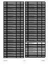
20021002 1-18-6 td603el q1602 inverter krc103m "npn" or nqsz0krc103m 4835 130 47909 inverter 2sc3400 "npn" or 2sc3400z 4835 130 47428 inverter ba1f4m-t qqsz00ba1f4m 4835 130 48204 q1603 buffer 2sc2785(f) "npn" or qqsf02sc2785 4835 130 47722 buffer 2sc2785(h) "npn" or qqsh02sc2785 4835 130 47722 buff...
Page 90
20021002 1-18-7 td603el r1251 carbon res. 1/4w 3.3k Ω ±5% or rcx4jatz0332 4835 110 57046 carbon res. 1/6w 3.3k Ω ±5% rcx6jatz0332 4835 111 37185 r1252 carbon res. 1/4w 1.5k Ω ±5% or rcx4jatz0152 4835 110 57186 carbon res. 1/6w 1.5k Ω ±5% rcx6jatz0152 4835 111 37306 r1253 carbon res. 1/4w 3.3k Ω ±5% ...
Page 91
20021002 1-18-8 td603el carbon res. 1/6w 27k Ω ±5% rcx6jatz0273 4835 111 37182 r1391 carbon res. 1/4w 100 Ω ±5% or rcx4jatz0101 4835 110 57003 carbon res. 1/6w 100 Ω ±5% rcx6jatz0101 4835 111 37161 r1392 carbon res. 1/4w 100 Ω ±5% or rcx4jatz0101 4835 110 57003 carbon res. 1/6w 100 Ω ±5% rcx6jatz010...
Page 92
20021002 1-18-9 td603el r1722 pcb jumper d0.6-p5.0 jw5.0t ---- --- ----- r1731 carbon res. 1/4w 47k Ω ±5% or rcx4jatz0473 4835 110 57189 carbon res. 1/6w 47k Ω ±5% rcx6jatz0473 4835 110 57189 r1732 pcb jumper d0.6-p5.0 jw5.0t ---- --- ----- r1751 carbon res. 1/4w 4.7k Ω ±5% or rcx4jatz0472 4835 110 ...
Page 93
20021002 1-18-10 td603el sensor cba mut cba h.V. Cba jk1701 rca jack(yellow) mtj-032-05b-20 jxrl010ly038 4835 265 97509 jk1702 rca jack(white) mtj-032-05b-22 jxrl010ly039 4835 265 97511 jk1703 rca jack(red) mtj-032-05a-21 jyrl010ly010 4835 265 97513 jk1801 mini jack hsj2000-01-010 or jysl010hd002 48...
Page 94
20021002 1-18-11 td603el # pp cap. 0.0027µf/1.6kv ±5% or ct3c272ms039 4835 121 47717 # metallized film cap. 0.0027µf/1.6kv ±5% ct3c272kf015 4835 121 47717 connectors cn571 connector base, 5p tv-50p-05-v3 or j3tvc05tg002 ---- --- ----- connector base, 5p rtb-1.5-5p j3rtc05jg001 ---- --- ----- diodes ...
Page 95
20021002 1-18-12 td603el crt cba r566 # carbon res. 1/4w 1.5 Ω ±5% rcx4jatz01r5 4835 110 57074 r569 carbon res. 1/4w 1.2 Ω ±5% rcx4jatz01r2 4835 110 57387 r572 carbon res. 1/4w 680 Ω ±5% or rcx4jatz0681 4835 110 57054 carbon res. 1/6w 680 Ω ±5% rcx6jatz0681 4835 111 37203 r573 carbon res. 1/4w 680 Ω...
Page 96
20021002 1-18-13 td603el junctoin a cba junctoin b cba mps cba power/av cba r521a carbon res. 1/4w 1.5k Ω ±5% rcx4jatz0152 4835 110 57186 r521b carbon res. 1/4w 1.5k Ω ±5% rcx4jatz0152 4835 110 57186 r522 carbon res. 1/4w 100 Ω ±5% or rcx4jatz0101 4835 110 57003 carbon res. 1/6w 100 Ω ±5% rcx6jatz01...
Page 97
20021002 1-18-14 td603el # electrolytic cap. 100µf/160v ±20% or ce2cmzptl101 4835 124 47698 # electrolytic cap. 100µf/160v ±20% w/ f ce2cmzntl101 4822 124 22663 c2617 # electrolytic cap. 470µf/35v ±20% or ce1gmasdl471 4835 124 47069 # electrolytic cap. 470µf/35v ±20% ce1gmastl471 4835 124 47069 c261...
Page 98
20021002 1-18-15 td603el # switching diode 1n4148 ndtz001n4148 4835 130 37048 d2631 switching diode 1ss133(t-77) or qdtz001ss133 4835 130 37235 switching diode 1n4148 ndtz001n4148 4835 130 37048 d2634 zener diode mtzjt-778.2b or qdtb0mtzj8r2 4835 130 37963 zener diode dz-8.2bsbt265 ndtb0dz8r2bs 4835...
Page 99
20021002 1-18-16 td603el buffer kta1266(gr) "pnp" or nqs40kta1266 4835 130 47422 buffer 2sa1015-gr(tpe2) "pnp" qqs102sa1015 4835 130 47399 q2601 # switching 2sk3407 qffz02sk3407 4835 130 48233 q2602 # limiter 2sc2120-o-tpe2 "npn" or qqs002sc2120 4835 130 47756 # limiter 2sc2120-y(tpe2) "npn" qqsy02s...
Page 100
20021002 1-18-17 td603el carbon res. 1/6w 47k Ω ±5% rcx6jatz0473 4835 110 57189 r2253 carbon res. 1/4w 9.1k Ω ±5% or rcx4jatz0912 4835 110 57165 carbon res. 1/6w 9.1k Ω ±5% rcx6jatz0912 4835 110 57165 r2254 carbon res. 1/4w 9.1k Ω ±5% or rcx4jatz0912 4835 110 57165 carbon res. 1/6w 9.1k Ω ±5% rcx6ja...
Page 101
20021002 1-18-18 td603el # carbon res. 1/6w 5.6k Ω ±5% rcx6jatz0562 4835 111 37199 r2634 carbon res. 1/4w 22k Ω ±5% or rcx4jatz0223 4835 110 57038 carbon res. 1/6w 22k Ω ±5% rcx6jatz0223 4835 111 37177 r2635 carbon res. 1/4w 10k Ω ±5% or rcx4jatz0103 4835 110 57026 carbon res. 1/6w 10k Ω ±5% rcx6jat...
Page 102
20021002 1-18-19 td603el filter cba # fuse stc4a125v u/ct or page20cw3402 4835 253 97153 # fuse 4.00a/125v pagg20cng402 4835 253 97153 fh2601 fuse holder msf-015 or xh01z00ly001 ---- --- ----- fuse holder fh-v-03078 xh01z00dk001 ---- --- ----- fh2602 fuse holder msf-015 or xh01z00ly001 ---- --- ----...
Page 103
Tb21 v501-1 l551 details for l551 and surrounding parts shinwha tape sgt-730 (white) shinwha tape sgt-730 (black) v501-3 v501-2 cl403 cl404 crt cba scotch tape #880 scotch tape #880 l551 a1x a1-7 a1-9 a1-8 tb6 l4 l4 a1-2 a1-3 a1-1 b6 l4 l4 b6 tl1 tl1 tl1 tl1 tl1 tl1 tl2 tl2 tb20 tb4 tb1 tl3 tl3 tl6 ...
Page 104
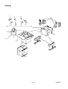
1-19-3 td603pex s2 s1 s3 s6 packing tape s7 x3 x4 x2 x8 x11 s4 x13 x1 tape x12 x10 x9 s4 s4 packing.
Page 105: Mechanical Parts List
20021002 1-20-1 td603ca mechanical parts list product safety note: products marked with a # have special characteristics important to safety. Before replacing any of these components, read care- fully the product safety notice in this service manual. Don't degrade the safety of the product through i...
Page 106
20021002 1-20-2 td603ca table 1 (v501 and l551 combination) note 1: purity and convergence adjustments must be performed following crt replacement. Refer to electri- cal adjustment instructions. Note 2: please confirm crt type no. On the crt warning label which is located on the crt. Then see table ...
Page 107
Philips consumer electronics company a division of philips electronics north america corporation technical service data service solutions group technical publications dept. P.O. Box 555, 401 e. Old andrew johnson hwy. Jefferson city,tn 37760 manual 5885 sec. 2: deck mechanism section standard mainte...
Page 108: Table of Contents
Table of contents [ deck mechanism section ] page standard maintenance . . . . . . . . . . . . . . . . . . . . . . . . . . . . . . . . . . . . . . . . . . . . . . . . . . . . . . . . . . . . . . . 2-1-1 service fixtures & tools. . . . . . . . . . . . . . . . . . . . . . . . . . . . . . . . . . . . ....
Page 109: Standard Maintenance
2-1-1 u25men standard maintenance service schedule of components notes: 1.Clean all parts for the tape transport (upper drum with video head / pinch roller / audio control head / full erase head) using 90% lsopropyl alcohol. 2.After cleaning the parts, do all deck adjustments. 3.For the reference nu...
Page 110
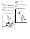
2-1-2 u25men cleaning cleaning of video head clean the head with a head cleaning stick or chamois cloth. Procedure 1.Remove the top cabinet. 2.Put on a glove (thin type) to avoid touching the upper and lower drum with your bare hand. 3.Put a few drops of 90% isopropyl alcohol on the head cleaning st...
Page 111: Service Fixture and Tools
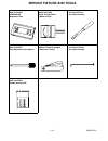
2-2-1 u25nfix-pc 4835 310 57025 vfms0001h6 alignment tape 4835 310 57043 back tension meter (made in usa) flat screw driver (purchase locally) 4835 310 57027 post adjustment screwdriver metric thickness gauges (purchase locally) lock screw driver (purchase locally) 4835 310 57034 head cleaning stick...
Page 112
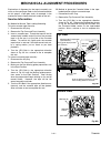
2-3-1 td603ma mechanical alignment procedures explanation of alignment for the tape to correctly run starts on the next page. Refer to the information below on this page if a tape gets stuck, for example, in the mechanism due to some electrical trouble of the unit. Service information a. Method for ...
Page 113
2-3-2 td603ma adjust the x value for maximum envelope. (pg. 2-3-3) (use alignment tape.) check to see that the tape is not creasing and that there is no slack on the supply and take-up side guide rollers. (use a blank tape.) adjust the height of the guide rollers (supply side and take-up side). (use...
Page 114
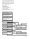
2-3-3 td603ma 1-a. Preliminary/final checking and alignment of tape path purpose: to make sure that the tape path is well stabilized. Symptom of misalignment: if the tape path is unstable, the tape will be damaged. Note: do not use an alignment tape for this proce- dure. If the unit is not correctly...
Page 115
2-3-4 td603ma 6. Press ch down button on the unit until the ctl waveform has shifted from its original position (not the position achieved in step 5, but the position of ctl waveform in step 4) by approximately -2msec. Make sure that the envelope is simply attenuated (shrinks in height) once ctl wav...
Page 116: Of Deck Mechanism
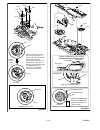
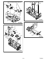
2-4-1 td603da disassembly/assembly procedures of deck mechanism before following the procedures described below, be sure to remove the deck assembly from the cabinet. (refer to cabinet disassembly instructions on page 1-8-1.) all the following procedures, including those for adjustment and replaceme...
Page 117
2-4-2 td603da (1): follow steps in sequence. When reassembling, follow the steps in reverse order. These numbers are also used as identification (location) no. Of parts in the figures. (2): indicates the part to start disassembling with in order to disassemble the part in column (1). (3): name of th...
Page 118
2-4-3 td603da [14] [13] [11] [10] [12] [7] [46] [8] [29] [40] [38] [37] [39] [42] [41] [43] [9] [33] [15] [35] [36] [34] fig. Dm1 top view fig. Dm2 bottom view [31] [19] [32] [24] [25] [27] [26] [23] [28] [21] [30] [20] [22].
Page 119
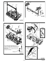
2-4-4 td603da [1] (s-1) (s-1) fig. Dm3 [2] pin a slots b pin c pin b pin d locking tab view for a pull up slide slot a slot a first, while pushing the locking tab as shown in the right, slide and pull up the right side on [2] to release pin a and pin b from the slots a. Then, remove pin c and pin d ...
Page 120
2-4-5 td603da pin of [12] pin of [10] grooves of [28] [28] when reassembling [10] and [12], confirm that pin of [10] and pin of [12] are in the grooves of [28] as shown. [11] [13] [12] a [10] (l-1) (p-3) adj. Screw (p-2) (l-2) view for a fig. Dm8 [14] [15] (s-9) (s-8) fig. Dm9 [17] [16] [18] (s-10) ...
Page 121
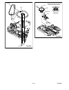
2-4-6 td603da [19] (s-11) cap belt fig. Dm11 [20] (c-1) a [21] portions a portions a view for a portions a on [21] must be set in the slot on [20] as shown. Fig. Dm12.
Page 122
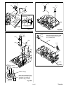
2-4-7 td603da [24] (c-5) (s-12) [25] [27] [26] [28] (c-4) (l-4) when reassembling [28], meet the first groove on [28] to the first tooth on [44] as shown. [28] top view first tooth on [44] first groove on [28] align [25] and [28] as shown. Bottom view [28] [25] pin of [33] pin of [30] position of mo...
Page 123
2-4-8 td603da [32] [30] [29] (l-5) (p-5) [31] refer to the alignment section, page 2-4-9. Fig. Dm15 (l-6) (p-7) (p-6) (c-6) [34] [40] [37] [35] [39] [33] [36] turn turn turn [38] (c-7) fig. Dm16 [41] [42] [43] (l-7) fig. Dm17 [45] [44] slide fig. Dm18 (p-8).
Page 124
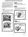
2-4-9 u25napm alignment procedures of mechanism the following procedures describe how to align the individual gears and levers that make up the tape loading/unloading mechanism. Since information about the state of the mechanism is provided to the system control circuit only through the mode switch,...
Page 125
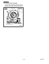
2-4-10 u25napm alignment 3 cam gear (a), rack assembly install the rack assembly so that the first tooth on the gear of the rack assembly meets the first groove on the cam gear (a) as shown in fig. Al4. Cam gear (a) first tooth first groove on the cam gear (a) alignment 3 top view gear on rack assem...
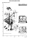
Page 126: Deck Exploded Views
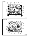
2-5-1 z11dexpc deck exploded views deck mechanism view 1 some ref. Numbers are not in sequence. B2 b35 b553 b410 b411 b494 b567 l1053 b74 b10 l1191 b73 b9 b12 b492 b11 b571 b37 b126 l1466 b501 b8 b121 b426 b560 l1450 l1051 l1467 mark description slidus oil #150 floil g-374g (blue grease) chassis ass...
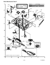
Page 127
2-5-2 z11dexpc deck mechanism view 2 some ref. Numbers are not in sequence. Bottom side (grease point) bottom side (grease point) view for a (grease point) b516 b559 a b52 b507 b488 b551 b133 b568 b569 b513 b502 b570 b491 b565 b417 l1151 b525 b522 b31 l1406 b148 b521 b520 b416 b518 b564 b585 b487 b5...
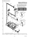
Page 128
2-5-3 z11dexpc deck mechanism view 3 mark description floil g-374g (blue grease) 1 2 3 4 g h i some ref. Numbers are not in sequence. B359 b529 b360 b303 b514 b555 b563 b300 b562 b482 b355 b354 b483 b425 l1461 l1341 l1341 l1321 b347 l1321 b361 b359 b529 b360 type b type a note: there are two differe...
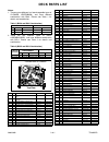
Page 129: Deck Parts List
20021002 2-6-1 td603dpl deck parts list notes: 1. There are two different, but interchangeable types of cleaner lever(b359), and have different combination with b361. Please see table 1 for details and combination. Table 1 (b359 and b361 combination) 2. There are two different types of rack assembly...
Page 130
20021002 2-6-2 td603dpl b568 d-2 bt arm mk10 0vm304417h 4835 402 97855 b569 e-2 cam holder f mk11 0vm305075 ---- --- ----- b570 e-2 cam rack spring(hi) mk11 0vm412923 ---- --- ----- b571 a-1 p.S.W f 6*2.55*0.5 0vm402629a ---- --- ----- b572 d-3 p.S.W cut 1.6x4.0x0.5t 0vm408485a ---- --- ----- b573 d...
Page 131
Philips consumer electronics company a division of philips electronics north america corporation service solutions group philips consumer electronics company service solutions group technical publications dept. P.O. Box 555, 401 e. Old andrew johnson hwy. Jefferson city,tn 37760
Page 132
Philips consumer electronics company a division of philips electronics north america corporation service solutions group philips consumer electronics company service solutions group technical publications dept. P.O. Box 555, 401 e. Old andrew johnson hwy. Jefferson city,tn 37760
Page 133
M anu al 58 85 color tv w it h built -in vcr /d v d p la y e r ma gna v o x 27m dtr10s.

