- DL manuals
- Panasonic
- Blu-ray Player
- DMP-BD75GA
- Service Manual
Panasonic DMP-BD75GA Service Manual
Summary of DMP-BD75GA
Page 1
©panasonic corporation 2011. Unauthorized copying and distribution is a violation of law. Order no.Chm1104018ce blu-ray disc player model no. Dmp-bd75ga dmp-bd75gc dmp-bd75gn dmp-bd75gt dmp-bd75gw dmp-bd75pu vol. 2 colour (k).......................Black type.
Page 2
2.
Page 3: Table of Contents
3 table of contents page page 1 safety precautions----------------------------------------------- 4 1.1. General guidelines ---------------------------------------- 4 1.2. Caution for fuse replacement--------------------------- 4 2 warning ------------------------------------------------------------...
Page 4: 1 Safety Precautions
4 1 safety precautions 1.1. General guidelines 1. When servicing, observe the original lead dress. If a short circuit is found, replace all parts which have been overheated or damaged by the short circuit. 2. After servicing, see to it that all the protective devices such as insulation barriers, ins...
Page 5
5 1.2.1. Micro fuse conducting check this unit uses the micro fuse. Check the micro fuse conducting using the tester at the check points below..
Page 6: 2 Warning
6 2 warning 2.1. Prevention of electrostatic discharge (esd) to electrostatic sensitive (es) devices some semiconductor (solid state) devices can be damaged easily by static electricity. Such components commonly are called elec- trostatic sensitive (es) devices. Examples of typical es devices are in...
Page 7
7 2.2. Service caution based on legal restrictions 2.2.1. General description about lead free solder (pbf) the lead free solder has been used in the mounting process of all electrical components on the printed circuit boards used for this equipment in considering the globally environmental conservat...
Page 8: 3 Service Navigation
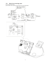
8 3 service navigation 3.1. Combination of multiple pressing on the remote control press multi-buttons (in combination) on the remote control simultaneously for operations, such as initialization or service mode, etc. There are no multiple pressing functions on the previous remote controls, thus, pl...
Page 9
9 3.2.2. Nondisclosure mode 1 (combination of multiple pressing: [6] [7] [yellow]) press and hold [6] [7] [yellow] on the remote control simultaneously for 5 sec., then [50 ret] is displayed on fl display window. 3.2.3. Nondisclosure mode 2 (combination of multiple pressing: [5] [9] [red]) press and...
Page 10: 4 Specifications
10 4 specifications power supply: ac220v-240v, 50/60hz (bd75ga/gc/gw) ac110v, 60hz (bd75gt) ac220v-240v, 50hz (bd75gn) ac110v-240v, 50/60hz (bd75pu) power consumption: approx. 12w (bd75ga/gc/gn/gt/gw) approx. 14w(bd75pu) in standby mode: approx. 0.2w (bd75ga/gc/gn/gw/pu) approx. 0.1w(bd75gt) in quic...
Page 11
11 bd-rom(sl/dl): (sl:single layer/dl;dual layer) compliant ver.1.3 bd-re(sl/dl): (sl:single layer/dl;dual layer) bd-mv bd-r(sl/dl): (sl:single layer/dl;dual layer) bd-mv dvd-rom(sl/dl): (sl:single layer/dl;dual layer) dvd-video dvd-r: dvd-video dvd-vr dvd-r(dl): dvd-video dvd-vr dvd-rw: dvd-video d...
Page 12: 5 Service Mode
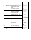
12 5 service mode 5.1. Self-diagnosis and special mode setting 5.1.1. Self-diagnosis functions self-diagnosis function provides information for errors to service personnel by “self-diagnosis display” when any error has occurred. U** and f** are stored in memory and held. You can check latest error c...
Page 13
13 f58 drive hardware error when drive unit error is detected, the event is saved in memory. No display no display f74 hdmi device key communica- tion error. This error is displayed when the information error is occurred at hdmi device key loading. No display f75 hdmi incompatible error (hdmi incomp...
Page 14
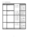
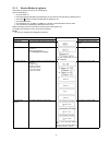
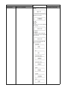
14 5.1.2. Special modes setting item fl display key operation mode name description front key rating password the audiovisual level setting password is initialized to level 8. While the unit is on, press and hold [ok], [b] and [y] on the remote control at the same time for more than 5 seconds. - "00...
Page 15
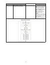
15 aging perform sequence of modes as * aging description shown below continually. Display following the then mode. Turn the power on. Press the [5] [9] and [r] button simultaneously for five seconds, then [70 ret] is displayed on fl. Press the [ ] button to select until [81 aig] is displayed on fl....
Page 16
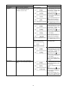
16 demonstration lock/unlock ejection of the disc is prohibited. The lock setting is effective until unlocking the tray and not released by main unit initialization of service mode. *when lock the tray. “lock” is displayed for 3 seconds. When the power is on, press and hold [ok], [b] and [y] on the ...
Page 17
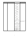
17 5.1.3. Service modes at a glance information necessary for service can be displayed. Service mode setting: 1. Turn the power on. 2. Press the [5] [9] and [r] button simultaneously for five seconds, then [70 ret] is displayed on fl. 3. Press the [ ] button to select until [80 srv] is displayed on ...
Page 18
18 bd drive last error bd drive error code display. 1. Error number is displayed for 5 seconds. 2. Time when the error has occurred is display for 5 seconds. Yy: year mm: month dd: day 3. Last drive error (1/2) is displayed for 5 seconds. 00 : bad disc 03 : bad disc 04 : bad disc or drive malfunctio...
Page 19
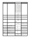
19 6. Disc maker id is displayed for 5 seconds. 7. Factor of drive error (hexadeci- mal) occurring is left displayed. In case that the maker cannot be identified, display is blackout. Item fl display key operation mode name description (remote controller key).
Page 20
20 8. When the last error doesn't exist . Cec (h) output the cec terminal high output of hdmi. Press [5] [5] in service mode. Cec (l) output the cec terminal low output of hdmi. Press [5] [6] in service mode. Manufacturing date read out the manufacturing date of the unit. Yy: year mm: month dd: day ...
Page 21: 6 Service Fixture & Tools
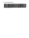
21 6 service fixture & tools * the above parts are supplied by avc-csc-spc. Part number description pcs compatibility rfkz0216 extension cable (digital p.C.B. - power p.C.B. / 23 pin) 1 same as bd60 series rfkz03d01ks lead free solder (0.3mm/100g reel) same as bd60 series rfkz06d01ks lead free solde...
Page 22
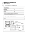
22 7 measurements and adjustments 7.1. Service positions note: for description of the disassembling procedure, see the section 9. (vol. 1) 7.1.1. Checking and repairing of digital p.C.B. Module.
Page 23
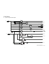
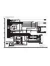
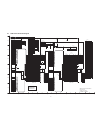
23 8 block diagram 8.1. Digital p.C.B. Regulator block diagram dmp-bd75ga/gc/gn/gt/gw/pu digital p.C.B. Regulator block diagram 22,23 p58001 p1102 (reg.Pw_dr5v) ic58302 vin vout 3 2 1 on[h] pw_x_sw5.9v 1 2 (reg.Pw_ad5v) ic56301 vin vout 3 2 1 on[h] from power p.C.B. From power p.C.B. 4 5 ic55005- / ...
Page 24
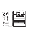
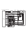
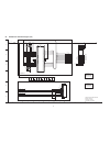
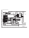
24 8.2. Digital (back end section) block diagram audio signal video signal ab1 usb_dm0 a7 gpio1 ab2 usb_dp0 ac3 gpio6 a12 ns_xtali b12 ns_xtalo x56301 5 7 1 ic59301 vin vout on[h] 3 2 1 pw_5.9v usb port p1103 ic51301 (8bit nand) ic52001 ddr sdram 1gbit 64m x 8bit nand flash memory 1 tc- nfd0-7 2 tc-...
Page 25
25 8.3. Ic pin terminal chart ic pin terminal chart ( tc 1 - tc 5) e m a n tr o p o n n i p o n n i p e m a n tr o p e m a n tr o p o n n i p o n n i p e m a n tr o p tc ic51001 / peaks-pro2 signal name ic52001 / sdram 1 tc ic51001 / peaks-pro2 signal name ic52001 / sdram 2 dmp-bd75ga/gc/gn/gt/gw/pu...
Page 26
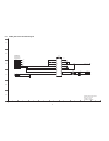
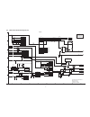
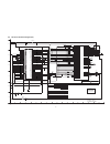
26 8.4. Digital (front end section) block diagram rfip rfip2 rfin rfin2 ina inb inc ind ine inf ing inh laser detector laser detector laser detector bd cd dvd fo/tr actuator spindle motor optical pick-up/traverse p55001 bd/dvd rf signal dvd focus and tracking signal bd focus and tracking signal cd m...
Page 27
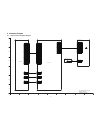
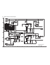
27 9 schematic diagram 9.1. Interconnection schematic diagram digital p.C.B. Bd drive power p.C.B. P55001 2 1 3 4 p1102 p58001 5 6 7 8 9 10 11 12 13 14 15 16 17 18 19 20 21 22 23 2 1 3 4 5 6 7 8 9 10 11 12 13 14 15 16 17 18 19 20 21 22 23 2 1 3 4 p1001 n a dmp-bd75ga/gc/gn/gt/gw/pu interconnection s...
Page 28
28 9.2. Audio_dac section schematic diagram f e d 1 c b a 9 8 7 6 5 4 3 2 audio_dac section schematic diagram (digital p.C.B(1/6)) dmp-bd75ga/gc/gn/gt/gw/pu 1 2 3 4 5 6 7 8 10 11 12 13 14 15 16 9 ic54004 c1ab00003352 smute mck bck lrck sdti aoutr dif cvdd vss2 vdd aoutl zdf vss1 cp vee cn c54016 1 c...
Page 29
29 9.3. Av section schematic diagram f e d 1 c b a 9 8 7 6 5 4 3 2 av section schematic diagram (digital p.C.B(2/6)) dmp-bd75ga/gc/gn/gt/gw/pu avss33_vdac_r e17 avdd33_vdac_x d19 avss33_vdac_x e19 avdd33_vdac_r d17 avss33_vdac_bg e18 avdd33_vdac_bg c19 ns_xtalq b12 ns_xtali a12 avss33_xtal d14 avdd1...
Page 30
30 9.4. Mtk section schematic diagram (1/2) 9 8 7 6 f 5 4 3 2 1 e d b a mtk section(1/2) schematic diagram dmp-bd75ga/gc/gn/gt/gw/pu (digital p.C.B(3/6)) nc nc nc nc nc nc /wp /we ale nc nc io0 io1 io2 nc io3 c n e l c nc nc vss vcc nc nc nc nc vss vcc prl nc /ce nc io4 r/b /se nc nc nc nc io5 io6 i...
Page 31
31 9.5. Mtk section schematic diagram (2/2) 17 16 15 14 f 13 12 11 10 9 e d b a mtk section(2/2) dmp-bd75ga/gc/gn/gt/gw/pu schematic diagram (digital p.C.B(3/6)) 1 ic51001 ic51001 ic51001 ic51001 ic51001 ic51001 ic51001 avdd33_usb_ip avdd33_usb_2p y3 aa3 avdd33_usb_ip avdd33_usb_2p y4 aa4 c51322 0.1...
Page 32
32 9.6. Digital_net section schematic diagram power_source section dmp-bd75ga/gc/gn/gt/gw/pu (digital p.C.B.(4/6 )) schematic diafram f e d 1 c b a 9 8 7 6 5 4 3 2 cka10 cka13 cka18 cka9 cka7 cka4 cka3 cka2 cka1 cka5 cka6 cka8 cka19 cka20 cka22 cka21 cka11 cka12 cka14 cka15 pw_x_sw5.9v 5 pw_x_sw5.9v...
Page 33
33 9.7. Ddr section schematic diagram f e d 1 c b a 9 8 7 6 5 4 3 2 dmp-bd75ga/gc/gn/gt/gw/pu ddr section schematic diagram (digital p.C.B.(5/6)) ddr3 chb m3 ba2 n8 ba1 m2 ba0 t3 a13 n7 a12(/bc) r7 a11 l7 a10(ap) r3 a9 t8 a8 r2 a7 r8 a6 p2 a5 p8 a4 n2 a3 p3 a2 p7 a1 n3 a0 a3 dqu7 dqu6 dqu5 dqu4 dqu3...
Page 34
34 9.8. Fe section schematic diagram (1/2) c55024 0.1 c55022 6.3v 220 f e d 1 c b a 9 8 7 6 5 4 3 2 fe section(1/2) dmp-bd75ga/gc/gn/gt/gw/pu (digital p.C.B.(6/6)) schematic diagram aux1 g_vr_cd g_vr_dvd g_md_dvd g_md_bd g_md_dvd g_md_bd g_vr_dvd g_vr_cd g_vr_dvd 1 2 ip55005 k5h252z00003 pw_dr5v ps ...
Page 35
35 9.9. Fe section schematic diagram (2/2) k6 v14 g6 fvref h6 havc a2 foip g4 trinc b3 foin g5 trind e1 ina e2 inb f1 inc f2 ind h3 ine h4 inf g2 ing g1 inh f4 trina g3 trinb d2 fpdodvd c1 fpdocd j3 rfin j4 rfip j1 rfip2 j2 rfin2 p2 fecfreq feoscen p1 fecmod r3 n2 fegainsw1 n3 fegainsw2 fegainsw3 p3...
Page 36
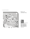
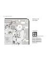
36 10 printed circuit board 10.1. Digital p.C.B. 10.1.1. Digital p.C.B. (component side) (1/4) f e d c56303 ic56301 1 3 5 4 c56302 rx56301 rx56302 1 3 6 4 q56302 cl56304 cks2 cl56303 cks15 cks18 cks16 c55122 c551 13 rl55119 rl55111 cl55020 rl55007 rl55008 rl55009 cl55018 cl55081 cl55050 cl55052 cl55...
Page 37
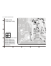
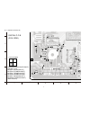
37 10.1.2. Digital p.C.B. (component side) (2/4) cl55050 cl55082 cl55008 c55014 c52021 c52015 c52047 c52007 c52017 c52046 c52014 c52003 c52004 c5131 1 c51312 c52020 c55020 c51323 ck51315 cl55048 rl55036 r59307 c51322 l55001 l55006 c51305 r59306 cl55035 c55046 c55100 r55046 r55047 c55059 c55061 c5507...
Page 38
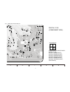
38 10.1.3. Digital p.C.B. (component side) (3/4) 5 4 3 2 1 c b a c51308 c52013 c52028 c52220 c52047 c52007 c5201 1 c52017 c52046 c52005 c52006 c52009 c52004 cka6 cka11 ic51002 1 5 cka20 rl52215 c51002 c58096 c51001 c59003 r59323 rx51001 qr51001 qr51002 qr51003 qr51006 qr51301 rx51303 rx58001 rx51002...
Page 39
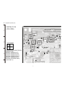
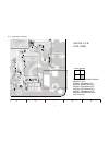
39 10.1.4. Digital p.C.B. (component side) (4/4) 9 8 7 6 5 c52028 c52220 c52047 c52007 c52017 c52046 c52005 c52006 c52223 c52009 c52004 c58089 ck51321 c59315 ic59301 5 7 4 1 c59317 c58302 r58042 qr58040 qr58041 ckc2 c58027 r58039 d58001 ckc4 r58043 r58536 c58026 ckc3 c58516 r58534 r58553 c58515 c585...
Page 40
40 10.1.5. Digital p.C.B. (foil side) (1/4) f e d ip55004 rl55016 rl55017 p55004 5 1 3 2 4 c55069 c55077 c55073 lb55001 c55047 c55034 rx55010 cl55074 cl55075 cl51314 cl51313 cl51312 ck51311 cl55030 cl55044 cl55045 cl55047 cl55065 rx55009 p55003 p55001 45 1 1 3 5 4 2 cl55002 c55012 c55013 c55082 cl55...
Page 41
41 10.1.6. Digital p.C.B. (foil side) (2/4) cl55030 cl55044 cl55045 cl55046 cl55043 cl55047 cl55041 cl55038 cl55037 cl55061 cl55039 cl55040 cl55042 cl55065 cl55059 cl55060 1 cl55007 cl55006 cl55005 c55033 p55002 1 2 3 4 c55035 rl55015 rl55013 cl55004 cl55003 cl55002 cl55001 c55012 c55013 c55082 cl55...
Page 42
42 10.1.7. Digital p.C.B. (foil side) (3/4) 5 4 3 2 1 c b a rl52037 rl52044 rl52043 rl52042 rl52041 ic52001 rl52038 rl52039 rl52040 c52221 c58532 c58093 ic58006 c58433 l58401 c58431 c58531 c58092 t59301 1 2 4 3 p58001 1 2 22 23 c52205 c58094 r52007 rl52036 rl52035 rl52034 rl52230 rl52229 rl52231 rl5...
Page 43
43 10.1.8. Digital p.C.B. (foil side) (4/4) 9 8 7 6 5 r56503 ck56008 ck56009 ck51308 ck51307 ck51331 ck51310 ck51340 ck51329 ck51309 ck56010 ck56011 ck54010 g56001 jk56001 cl56306 c54019 c54022 rx54002 ck56006 ck56005 ck56004 c54018 r56007 ic54004 1 8 9 16 r51361 c54016 c54020 r51330 rl52221 rl52222...
Page 44
44 10.1.9. Digital p.C.B. Address information transistors digital p.C.B. Transistor-resistors address information c......Component side f......Foil side integrated circuits test points q56301 e-3 d-2 c c q55002 e-3 c q56302 q58006 a-2 f ic51001 d-5 f ic51002 b-4 c ic51301 b-6 f ic52001 c-3 f ic52201...
Page 45
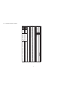
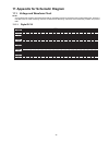
45 11 appendix for schematic diagram 11.1. Voltage and waveform chart note: circuit voltage and waveform described herein shall be regarded as reference information when probing defect point, because it may differ from an actual measuring value due to difference of measuring instrument and its measu...
Page 46
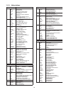
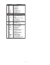
46 11.1.2. Abbreviations initial/logo abbreviations a a0~up aclk ad0~up adata ale amute areq arf asi aso async address audio clock address bus audio pes packet data address latch enable audio mute audio pes packet request audio rf servo amp inverted input servo amp output audio word distinction sync...
Page 47
47 initial/logo abbreviations t te tibal tid tin tip tis tpsn tpso tpsp trcrs tron trson tracking error balance control balance output 1 balance input balance input balance output 2 op amp input op amp output op amp inverted input track cross signal tracking on traverse servo on initial/logo abbrevi...
Page 48
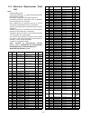
48 11.2. Electrical replacement parts list notes: *important safety notice: components identified by mark have special character- istics important for safety. Furthermore, special parts which have purposes of fire-retardant (resistors), high-quality sound (capacitors), low-noise (resistors), etc. Ar...
Page 49
49 c55026 f1j1a106a024 10v 10u 1 c55030 f1j0j2260004 6.3v 22u 1 c55031 f1g1e222a086 25v 2200p 1 c55032 f1j0j2260004 6.3v 22u 1 c55033 f1g1c104a077 16v 0.1u 1 c55034 f2g0j221a065 6.3v 220u 1 c55035 f1g1c104a077 16v 0.1u 1 c55042 f2g0j221a065 6.3v 220u 1 c55043 f1g1a104a012 10v 0.1u 1 c55046 f1h0j2250...
Page 50
50 l58501 g1c4r7z00014 coil 1 lb55001 j0jyc0000107 coil 1 lb55002 j0jyc0000107 coil 1 lb55004 j0jhc0000109 coil 1 lb56002 j0jyc0000070 coil 1 lb56306 j0jyc0000070 coil 1 lb56307 j0jyc0000070 coil 1 lb56308 j0jyc0000070 coil 1 lb56501 j0jyc0000070 coil 1 lb56502 j0jyc0000070 coil 1 lb56503 j0jyc00000...

