- DL manuals
- Tadpole
- Laptop
- SPARCbook 3 series
- Reference Manual
Tadpole SPARCbook 3 series Reference Manual
Summary of SPARCbook 3 series
Page 1
Series technical reference manual 980327-02 3 s3gx_trmbook page i friday, september 19, 1997 11:39 am.
Page 2: Trademarks
Ii sparcbook 3 technical reference manual trademarks all rights reserved. This product or document is protected by copyright and distributed under licenses restricting its use, copying, distribution and decompilation. No part of this product or document may be reproduced in any form by any means wit...
Page 3: Contents
Iii contents about this guide ix document summary . . . . . . . . . . . . . . . . . . . . . . . . . . . . . . . . . . . . . . . . . . . . . . . . . . . . .X definitions . . . . . . . . . . . . . . . . . . . . . . . . . . . . . . . . . . . . . . . . . . . . . . . . . . . . . . . . . . . Xi logic stat...
Page 4: Chapter 2
Iv 1.13 modem interface . . . . . . . . . . . . . . . . . . . . . . . . . . . . . . . . . . . . . . . . . . . . . . 1-14 1.14 microcontroller subsystem . . . . . . . . . . . . . . . . . . . . . . . . . . . . . . . . . . . . . . 1-15 chapter 2 the sparc cpu 2.1 sparc architecture overview . . . . . ....
Page 5: Chapter 5
V chapter 5 scsi controller 5.1 connecting scsi devices . . . . . . . . . . . . . . . . . . . . . . . . . . . . . . . . . . . . . . . . . 5-2 5.2 ncr53c9x scsi controller . . . . . . . . . . . . . . . . . . . . . . . . . . . . . . . . . . . . . . 5-2 5.2.1 53c9x register set . . . . . . . . . . . . ...
Page 6: Chapter 9
Vi 8.2.3 sbus interface . . . . . . . . . . . . . . . . . . . . . . . . . . . . . . . . . . . . . . . . . . . . . . . 8-3 8.2.4 dbri programming model . . . . . . . . . . . . . . . . . . . . . . . . . . . . . . . . . . . . 8-4 8.2.5 dbri internal registers . . . . . . . . . . . . . . . . . . . . . ....
Page 7
Vii 11.4 ramdac . . . . . . . . . . . . . . . . . . . . . . . . . . . . . . . . . . . . . . . . . . . . . . . . . . . 11-21 11.4.1 ramdac host interface . . . . . . . . . . . . . . . . . . . . . . . . . . . . . . . . . . . . . 11-22 11.4.2 control register accesses . . . . . . . . . . . . . . . . . ...
Page 8
Viii s3gx_trmbook page viii friday, september 19, 1997 11:39 am.
Page 9: About This Guide
About this guide the sparcbook 3 technical reference manual is written for the hardware engineer wishing to carry out service or repairs, and at the software engineer wishing to implement hardware drivers. It is assumed that you are familiar with the operation of sparcbook 3, as detailed in the spar...
Page 10: Document Summary
X document summary the sparcbook 3 technical reference manual comprises the following chapters: • chapter 1 , architecture overview, discusses the main features of the sparcbook 3 and introduces the main hardware devices that provide control over the sparcbook 3’s operations. The internal architectu...
Page 11: Definitions
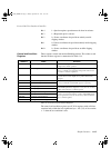
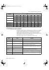
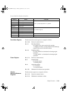
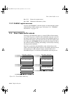
Xi definitions the following conventions are used in the sparcbook 3 technical reference manual: logic states the terms clear or low indicate that the signal being discussed is at the logic level ‘0’. The terms set or high indicate that the signal being discussed is at the logic level ‘1’. The term ...
Page 12: Solaris Commands
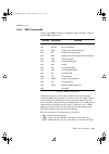
Xii solaris commands information displayed on your sparcbook screen by the solaris operating system is shown in courier font. Courier is also used to describe system utilities and commands. For example: the mail system will inform you when there is incoming mail from another user. You have mail bold...
Page 13: Architecture Overview
Architecture overview 1 1 this chapter discusses the architecture of the sparcbook 3. It describes the main system components and how they are packaged together to deliver workstation-class performance in a compact notebook form factor. S3gx_trmbook page 1 friday, september 19, 1997 11:39 am.
Page 14: 1.1
1-2 architecture overview introduction 1.1 introduction at the heart of the sparcbook 3 design concept is the tadpole advanced notebook architecture (ana). This defines a set of goals and guidelines to which the sparcbook 3 range of systems are designed. It is a modular approach which results in a s...
Page 15: 1.2.3
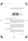
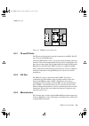
Architecture overview 1-3 main components are fixed together. When the two boards are correctly assembled, the cpu heatsink is brought into contact with the system’s magnesium base casting to provide effective heat dissipation, as shown in figure 1-1. 1.2.3 microcontroller module the microcontroller...
Page 16: 1.3
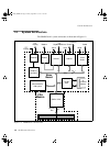
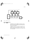
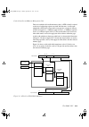
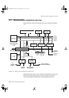
1-4 architecture overview system architecture 1.3 system architecture the sparcbook 3 system architecture is illustrated in figure 1-2. Figure 1-2 sparcbook 3 architecture 64 memory bus macio slavio ts102 asic microcontroller subsystem isdn/ audio graphics controller ramdac 2x pcmcia sockets serial ...
Page 17: 1.4
Architecture overview 1-5 processor 1.4 processor the cpu used in the s3tx is the turbosparc and the cpu used in the s3xpand s3gx is the microsparc ii. The turbosparc cpu provides the following key features: • sparc compliant v8 integer unit core • sparc reference memory management unit • floating p...
Page 18: 1.5
1-6 architecture overview main system buses 1.5 main system buses the sparcbook 3 architecture is based around three main buses conventional for sparc-based workstations. These are the memory bus which connects the cpu to the main memory; the sbus which connects the cpu to the major i/o devices; and...
Page 19: 1.5.3
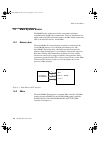
Architecture overview 1-7 main system buses the microsparc ii provides an sbus master and slave interface which enables the i/o devices with integrated dma capability to gain access to the main memory without encroaching unduly on processor bandwidth. Sbus master and slave operations can be single c...
Page 20: 1.6
1-8 architecture overview dram 1.6 dram the sparcbook 3 provides two simm sites which support a range of different capacity modules. The simm sites accommodate 72-pin units, which must be fitted in matched pairs to provide a full width 64-bit data interface for the microsparc ii. The simms are each ...
Page 21: 1.7
Architecture overview 1-9 slow i/o subsystem 1.7 slow i/o subsystem the slow i/o subsystem is managed by an ncr89c105 slavio. The slavio is an application specific integrated circuit (asic), designed as part of a two-chip set with the ncr89c100 macio, which provides two serial channels, keyboard and...
Page 22: 1.7.3
1-10 architecture overview fast i/o subsystem 1.7.3 interrupt controller the interrupt controller co-ordinates all on-board interrupt functions. These include all internal sources and a number of signals from elsewhere within the system. The microsparc ii uses a 4-bit priority encoded interrupt mech...
Page 23: 1.8.2
Architecture overview 1-11 fast i/o subsystem 1.8.2 ethernet controller the ethernet controller provides a 10mbit/sec networking interface. The design features an at&t serial interface encoder to provide the standard aui interface through a 26-way high density connector. An aui cable and an ethernet...
Page 24: 1.9
1-12 architecture overview graphics and video subsystem 1.9 graphics and video subsystem the graphics and video subsystem comprises the weitek p9100 user interface controller, an ibm rgb528 palette dac (ramdac), and a framebuffer provided by a 2mbyte array of video ram (vram) devices. All display in...
Page 25: 1.10
Architecture overview 1-13 mk48t08 rtcram in 256 colors from a palette of 262144. The ramdac can be software configured to support display resolutions of up to 1280 x 1024 in 256 colors (from a choice of 16m) on external monitors. 16 bit and 24 bit true color imaging modes are also supported on some...
Page 26: 1.12
1-14 architecture overview pcmcia controller fifos allow burst data transfers to be performed on the sbus. Large amounts of isdn or audio information can be moved to and from the sbus with a minimum of processor overhead. The data is formatted by the isdn controller into a composite digital serial s...
Page 27: 1.14
Architecture overview 1-15 microcontroller subsystem the modem supports a number of high level functions. It implements dtmf dialing, call progression, and is controlled via an enhanced “at” command set. The data standards supported include v.22 bis, v.23, v.32, v.32 bis, v.42, and v.42 bis. In addi...
Page 28
1-16 architecture overview microcontroller subsystem s3gx_trmbook page 16 friday, september 19, 1997 11:39 am.
Page 29: The Sparc Cpu
The sparc cpu 2 2 2 processing power for all sparcbook 3 models is provided by sparc processors. In the case of he s3xp and s3gx microsparc ii is used; in the case of the s3tx turbosparc is used. This chapter provides a general overview of sparc cpu. For further information, please refer to appendix...
Page 30: 2.1
2-2 the sparc cpu sparc architecture overview 2.1 sparc architecture overview the sparc processor is a highly integrated device which provides the following features: • sparc compliant v8 integer unit core • sparc reference memory management unit • meiko floating point unit • 16 kbyte instruction ca...
Page 31: 2.2
The sparc cpu 2-3 integer unit the sparc cpu is a risc (reduced instruction set computer) based processor which uses a simplified command set to carry out operations. It is able to execute most instructions within a single clock cycle. The high performance of the sparc cpu is enhanced by the ability...
Page 32: 2.2.3
2-4 the sparc cpu integer unit the arithmetic, logical and shift instructions compute a result that is a function of one or two source operands and then place the result non-destructively in a register. The control transfer instruction category includes jumps, calls, traps, and branches. Control tra...
Page 33: 2.2.4
The sparc cpu 2-5 integer unit the iu supports both asynchronous traps (interrupts) and synchronous traps (error conditions and trap instructions). Traps transfer control to an offset within the trap table. The base address of the table is specified by the trap base register and the offset is a func...
Page 34: 2.2.6
2-6 the sparc cpu integer unit window, and is incremented when the processor returns to the previous window. Register windows can be marked as invalid in the wim register, and interrupts can be enabled to signal when movement into an invalid window is caused by an instruction. 2.2.6 iu control regis...
Page 35: 2.3
The sparc cpu 2-7 floating point unit 2.3 floating point unit the sparc fpu is designed to execute all single- and double-precision sparc version 8 floating point instructions except fsmuld. All other fp instructions cause an unimplemented floating point operation trap. The fpu contains a 32x32-bit ...
Page 36: 2.3.1
2-8 the sparc cpu cache controller and memory management unit 2.3.1 floating point registers the fpu contains thirty-two 32-bit floating-point f registers, as illustrated in figure 3-8. These form a 32x32-bit register file. The contents of these registers are transferred to and from external memory ...
Page 37: 2.4.1
The sparc cpu 2-9 cache controller and memory management unit 2.4.1 translation lookaside buffer the memory management unit (mmu) conforms to the standard sparc architecture definition for memory management. The mmu provides virtual to physical address translation using a translation lookaside buffe...
Page 38
2-10 the sparc cpu cache controller and memory management unit ptp this bit, when set, indicates that a page table pointer is contained in this entry page table field this field can contain a pte, ptp or i/o pte. It can be read and written using asi 0x06 (25 bits). Page table entry the pte defines t...
Page 39: 2.4.2
The sparc cpu 2-11 cache controller and memory management unit page table pointer the ptp contains the physical address of a page table in memory, and can be found in the context table, or in a level 1 or 2 page table. Page tables are loaded into the tlb during tablewalks, and are removed by tablewa...
Page 40
2-12 the sparc cpu cache controller and memory management unit the context table pointer register provides a pointer to the context table, and the context register provides an index to the root pointer, which in turn points to a level 1 page table. Index 1 from the virtual address selects an entry w...
Page 41
The sparc cpu 2-13 cache controller and memory management unit the level at which a table walk terminates (that is, a pte is found) is related to the size of addressing region associated with the entry. A table walk which finds a pte in the context table corresponds to a region of 4gbytes. A pte cor...
Page 42: 2.5
2-14 the sparc cpu memory interface 2.5 memory interface the sparc provides a 64-bit memory interface which supports up to 128mbytes of system memory. The memory is composed of four banks of up to 32mbytes each. Different density devices are supported, allowing the sparcbook 3 to be fitted with a ra...
Page 43: 2.8.1
The sparc cpu 2-15 sbus controller 2.8.1 programmed i/o programmed i/o transactions consist of an sbus slave cycle only, with address translations being carried out before bus acquisition. The processor executes loads and stores to transfer data between it and devices on the sbus (in i/o space). The...
Page 44
2-16 the sparc cpu sbus controller s3gx_trmbook page 16 friday, september 19, 1997 11:39 am.
Page 45: Memory Map and Interrupts
Memory map and interrupts 3 3 3 this chapter describes the addressing architecture and interrupt architecture of sparcbook 3. The slavio incorporates an interrupt controller and is used to coordinate all on-board interrupts. These include interrupts from devices on the board and interrupts from slav...
Page 46: 3.1
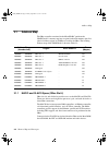
3-2 memory map and interrupts address map 3.1 address map the sbus controller contained in the microsparc partitions the sparcbook 3’s memory map into a region for the main memory plus five physical address regions of 256mbytes each for the sbus. The resulting memory map of the sparcbook is shown in...
Page 47
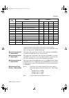
Memory map and interrupts 3-3 address map the map for sbus slot 4 is as shwon in table 3-2. The macio provides processor accessible control ports for dma related operations, for parallel port operations, for scsi operations and for network interface control. The function and access sizes of these lo...
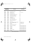
Page 48
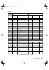
3-4 memory map and interrupts address map offset range (hexadecimal) resource accessibility 1f00000 1ffffff slavio system controller and status register word 1e00000 1efffff slavio interrupt controller word 1d00000 1dfffff slavio counter/timers word, doubleword 1c00000 1cfffff slavio reserved 1b0000...
Page 49: 3.1.2
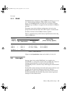
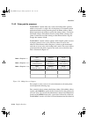
Memory map and interrupts 3-5 interrupts 3.1.2 dram the dram address multiplexers support simm units with up to 11 x 11 or (12 x 10) row/column multiplex (1mbit, 4mbit, and most 16mbit devices). Each simm module can contain one or two banks of memory. Simm sizes up to 64mbytes are supported, with a ...
Page 50
3-6 memory map and interrupts interrupts the interrupts in sparcbook 3 can be considered as belonging to three categories: slavio interrupts, macio interrupts, and sbus interrupts. The slavio interrupts include those from the internal serial ports and timers and the software interrupts. The macio in...
Page 51: 3.2.1
Memory map and interrupts 3-7 interrupts 3.2.1 interrupt control the slavio provides a number of interrupts status and control locations. The processor group provides interrupt pending information and control over software interrupts. The system group provides enable and clearing control over the in...
Page 52
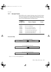
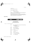
3-8 memory map and interrupts interrupts softint(15:1) software interrupt hardint(15:1) hardware interrupt ic interrupt level 15 clear writing a ‘1’ to any of the softint bits or ic bit in the interrupt clear pseudo-register clears the associated interrupt. The set soft int pseudo-register is used t...
Page 53: 3.3
Memory map and interrupts 3-9 ncr89c105 slavio configuration control bit 17 reserved bit 16 e – ethernet interrupt bit 15 bit s – serial port interrupt (slavio) bit 14 k – keyboard/mouse interrupt bits 13:07 sbus irq (7:1) bits 06:00 reserved 3.3 ncr89c105 slavio configuration control 3.3.1 slavio c...
Page 54: 3.3.2
3-10 memory map and interrupts ncr89c105 slavio configuration control bit 2 d - density select source (1 = 82077 density select, 0 = 82077 motor enable #2). - this bit determines which signal drives the external density select pin (fpy_densel). Bit 1 m - modem ring select. When this bit is set to 1,...
Page 55: 3.3.3
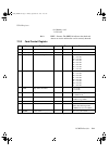
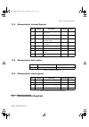
Memory map and interrupts 3-11 ncr89c105 slavio configuration control note all bits in the diagnostic message register are unaffected by system resetbut contains random information after a power-on reset. 3.3.3 miscellaneous system functions the ncr89c105 contains two 8-bit auxiliary i/o registers: ...
Page 56
3-12 memory map and interrupts ncr89c105 slavio configuration control power down control (aux 2) register all bits are cleared to 0 on system reset. Bits 7:6 reserved. These bits should be masked, and their values should be discarded by the software. These bits can be read and written to, but the va...
Page 57
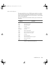
Memory map and interrupts 3-13 ncr89c105 slavio configuration control modem register the ncr89c105 can directly support the ri (ring indicate) bit output of a modem, when it is configured for modem use. This mode uses the msi_irq_ input pin for sensing modem ri. When the modem mode and the modem int...
Page 58
3-14 memory map and interrupts ncr89c105 slavio configuration control s3gx_trmbook page 14 friday, september 19, 1997 11:39 am.
Page 59: Serial Interface
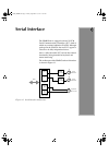
Serial interface 4 4 4 the sparcbook is equipped with two z85c30 serial communications controllers (scc), both of which are contained within the slavio. Although packaged in the slavio, the two sccs appear to software to be fully independent devices. One is a fully functional scc and one has reduced...
Page 60: 4.1
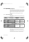
4-2 serial interface serial channel assignment 4.1 serial channel assignment there are four serial channels on the sparcbook, which are controlled by sccs within the slavio. Each channel provides a control interface. Serial channels a and b are controlled via the full-function scc; the keyboard and ...
Page 61: 4.2
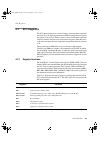
Serial interface 4-3 scc registers 4.2 scc registers the scc internal registers are accessed using a register pointer to perform selection. First, the register pointer bits in wr0 are programmed to specify the register to be accessed. Then, a read or a write is performed at the same address to trans...
Page 62
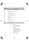
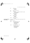
4-4 serial interface scc registers wr0 bits 7:6 resets 00 = null 01 = reset rx crc checker 10 = reset tx crc generator 11 = reset tx underrun/oem latch bits 5:3 commands 000 = null 001 = point high (reg 8-15 select) 010 = reset external/status interrupts 011 = send abort (sdlc mode) 100 = enable int...
Page 63
Serial interface 4-5 scc registers wr1 bit 7 wait/dma request enable bit 6 wait/dma request bit 5 wait/dma request on rx/tx bit 4:3 receive interrupt control 00 = interrupt disable 01 = interrupt on first char or special condition 10 = interrupt on all chars or special condition 11 = interrupt on sp...
Page 64
4-6 serial interface scc registers 00 = sync modes enabled 01 = 1 stop bit/character 10 = 1.5 stop bits/character 11 = 2 stop bits/character bit 1 parity even/odd bit 0 parity enable wr5 – transmit parameters and control bit 7 dtr bits 6:5 bits/character 00 = 5 bits 01 = 7 bits 10 = 6 bits 11 = 8 bi...
Page 65
Serial interface 4-7 scc registers 00 = nrz 01 = nrzi 10 = fm1 11 = fm0 bit 4 active on poll bit 3 mark/flag on idle bit 2 abort/flag on idle bit 1 loop mode bit 0 6-bit/8-bit sync wr11 – clock mode control bit 7 rtxcb xtal/no xtal bits 6:5 receive clock source 00 - 01 = reserved 10 = baud rate gene...
Page 66
4-8 serial interface scc registers wr15 – external/status interrupt control bit 7 break/abort interrupt enable bit 6 tx underrun/eom interrupt enable bit 5 cts enable bit 4 sync/hunt enable bit 3 dcd interrupt enable bit 2 reserved (write 0) bit 1 zero count interrupt enable bit 0 reserved (write 0)...
Page 67
Serial interface 4-9 scc registers bit 3 channel a ext/stat bit 2 channel b rx bit 1 channel b tx bit 0 channel b ext/stat rr10 – miscellaneous status bit 7 one clock missing bit 6 two clocks missing bit 4 loop sending bit 1 on loop other bits 0 rr15 – external/status interrupt status bit 7 break/ab...
Page 68: 4.3
4-10 serial interface baud rate clocks 4.3 baud rate clocks a 19.66 mhz clock signal generated by the macio is used to derive a baud rate clock for all of the sccs. This is divided by four before being fed to the sccs at 4.915 mhz. The baud rate can be changed by loading different time constants (wh...
Page 69: Scsi Controller
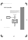
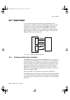
Scsi controller 5 5 5 the macio incorporates an enhanced ncr53c90 fast scsi controller (fsc), which supports scsi-2 operations at up to 10 mbytes/sec running synchronously. Scsi transfers are supported by the macio’s integral dma controller. Figure 5-1 scsi architecture ncr 53c90 sbus scsi scsi cont...
Page 70: 5.1
5-2 scsi controller connecting scsi devices 5.1 connecting scsi devices the sparcbook provides a 30-pin high density (hosiden style) connector, to which you can connect the supplied scsi adapter cable. This cable provides a 50-way high density scsi-2 connector that can be used to make connection to ...
Page 71
Scsi controller 5-3 ncr53c9x scsi controller there follows a brief description of the fsc registers. A detailed programming description of the device is beyond the scope of this manual and the user should refer to the bibliography at the rear of this document. Command register the command register i...
Page 72
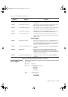
5-4 scsi controller ncr53c9x scsi controller command register value command interrupt 7 6 5 4 3 2 1 0 immediate commands x 0 0 0 0 0 0 0 no operation no x 0 0 0 0 0 0 1 flush fifo no x 0 0 0 0 0 1 0 reset 53c90a device no x 0 0 0 0 0 1 1 reset scsi bus no disconnect commands x 1 0 0 0 0 0 0 reselect...
Page 73
Scsi controller 5-5 ncr53c9x scsi controller status register the status register contains the device and interrupt status flags. The status register should always be read prior to reading the interrupt status register which will cause bits to clear. The status register contains error, transfer count...
Page 74
5-6 scsi controller ncr53c9x scsi controller bit 1 selected with atn bit 0 selected configuration registers the con1, con2 and con3 registers allow various operating modes to be set up. Con1 is used to control the slow cable mode, parity enable and test, and the 3-bit scsi host id. Con2 provides con...
Page 75: 5.3
Scsi controller 5-7 dma support 5.3 dma support the scsi controller is provided with dma support by one channel of the macio integral dma controller. Between the fsc and sbus the macio provides a 64-byte deep fifo (d-fifo) which is bypassed by cpu accesses to the fsc’s registers. 5.3.1 dma transfers...
Page 76
5-8 scsi controller dma support s3gx_trmbook page 8 friday, september 19, 1997 11:39 am.
Page 77: Ethernet Interface
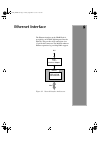
Ethernet interface 6 6 6 the ethernet interface on the sparcbook is provided by an ncr92c990 integrated into the macio. This provides aui connections via a 15-pin d-shell connector. The macio enhances ethernet operations by providing dma support. Figure 6-1 network interface architecture ncr 92c990 ...
Page 78: 6.1
6-2 ethernet interface ncr92c990 overview 6.1 ncr92c990 overview the ncr92c990 is a lan controller which supports the parameters for an ieee 802.3 network interface. 6.1.1 bus interface the lan controller operates as a bus master or a bus slave device. As a slave, it provides a 16-bit control interf...
Page 79: 6.2
Ethernet interface 6-3 lan controller registers 6.2 lan controller registers access to the lan controller’s internal registers is gained via two 16-bit locations, the register data port (rdp) and register address port (rap). The rap is loaded with an index to the required register, and then the regi...
Page 80: 6.2.3
6-4 ethernet interface lan controller registers err error – a logical “or” of bab, ce, miss and me bab babble – transmitter timeout error ce collision error miss missed packet me memory error – lan controller unable to access memory as bus master. Rint receiver interrupt – set when a packet is recei...
Page 81: 6.2.4
Ethernet interface 6-5 dma support for network operations 6.2.4 control and status register 3 this register is used to set the lan controller operating parameters to suit its hardware environment. It is programmed by the resident firmware during system start-up and should not be changed. 6.3 dma sup...
Page 82
6-6 ethernet interface dma support for network operations s3gx_trmbook page 6 friday, september 19, 1997 11:39 am.
Page 83: Pcmcia Interface
Pcmcia interface 7 7 7 the pcmcia inteface is controlled by a custom designed asic (application specific integrated circuit), the ts102. The ts102 provides support for two pcmcia cards and, in addition, an interface between the cpu and microcontroller subsystem which provides battery management, key...
Page 84: 7.1
7-2 pcmcia interface ts102 architecture overview 7.1 ts102 architecture overview the general architecture of the ts102 asic is illustrated in figure 8-5. 7.1.1 sbus interface the ts102 provides an ieee-p1496 compliant 32-bit slave interface, with separate address spaces for pcmcia memory accesses an...
Page 85: 7.1.2
Pcmcia interface 7-3 ts102 architecture overview the ts102 also features a read-ahead capability. Setting the read-ahead bit in the ts102 card register causes the ts102 to pre-fetch an additional 8 words a of data after each 8 word read from the card, starting from the address used in the last trans...
Page 86: 7.2
7-4 pcmcia interface ts102 memory mapping port status register, and also asserts an interrupt request to the microcontroller. The microcontroller read of the receive register clears the cpu write busy bit and the interrupt request. There is a similar protocol for transfers from the microcontroller t...
Page 87: 7.2.2
Pcmcia interface 7-5 ts102 memory mapping asserts its wait signal, the ts102 slave interface responds with a retry acknowledgment to the master, and then continues with the pcmcia transfer cycle. Similarly, burst accesses to slow pcmcia cards can cause a single burst access to take longer than 10 µ ...
Page 88: 7.2.3
7-6 pcmcia interface ts102 memory mapping with an iois16* acknowledgement. The ts102 monitors the iois16* signal during i/o accesses in order to decide how many pcmcia accesses to perform for a given master cycle. 7.2.3 slavio expansion interface the slavio controls access to the boot eprom and para...
Page 89: 7.3
Pcmcia interface 7-7 ts102 registers intended primarily for recovery from accidental erasure of the boot prom contents, but may also be used for such applications as field diagnostics, or even os upgrades. It is also necessary to inhibit the generation of the sbus select to the slavio device when bo...
Page 90: 7.3.1
7-8 pcmcia interface ts102 registers the pcmcia specification relies on software negotiation between the host system and each card to configure the hardware interface. As a result of this negotiation, some signals on the pcmcia interface can, if required, be redefined. This is handled via the ts102 ...
Page 91: 7.3.2
Pcmcia interface 7-9 ts102 registers i/o cards replace the two battery voltage signals with card status changed and audio waveform input signals. In this case the battery status changed interrupt becomes a card status changed interrupt, and the card status must then be read from the card. 7.3.2 card...
Page 92
7-10 pcmcia interface ts102 registers request is not automatically masked when the card is not i/o. The interrupt request should normally be explicitly masked when the card is not i/o using the interurpt mask bit in the card interrupt register. Bit 11 lvl – irq leve/edge control. This bit controls w...
Page 93: 7.3.3
Pcmcia interface 7-11 ts102 registers 0 = memory card 1 = i/o card bit 0 pres – present. The pres bit indicates that both card detects are active and that the card is correctly inserted. 7.3.3 card control register bit name function asserted reset comments 1:0 aa[25:24] attribute address a(25:24) 3:...
Page 94: 7.3.4
7-12 pcmcia interface microcontroller registers 7.3.4 microcontroller interrupt register 7.3.5 microcontroller data register 7.3.6 microcontroller status register 7.4 microcontroller registers bit name function asserted reset 0 txe_req transmit fifo empty inter- rupt request 1 0 1 txnf_req transmit ...
Page 95
Pcmcia interface 7-13 microcontroller registers the microcontroller has access to ts102 registers within its own address space. The content of these registers and protocols for use are under the control of software programmed into the microcontroller’s onboard rom during system manufacture. The regi...
Page 96
7-14 pcmcia interface microcontroller registers s3gx_trmbook page 14 friday, september 19, 1997 11:39 am.
Page 97: Isdn and 16-Bit Audio
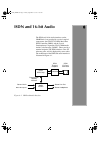
Isdn and 16-bit audio 8 8 8 the isdn and 16-bit audio interfaces on the sparcbook 3 are provided by a pair of coupled components: the at&t t7259 dual basic rate isdn controller (dbri); and the crystal semiconductor corporation cs4215 multimedia audio coder-decoder (codec). These provide a terminal e...
Page 98: 8.1
8-2 isdn and 16-bit audio isdn overview 8.1 isdn overview the integrated services digital network (isdn) is an advanced telephone system which allows computers to communicate together at a higher data rate than they could using a modem. Information carried on the isdn is digital and uses a circuit s...
Page 99: 8.2.1
Isdn and 16-bit audio 8-3 dbri overview 8.2.1 te and nt ports the te port provides the basic network connection to the isdn. The nt port is not used in sparcbook 3. An internal fifo buffer is used as a pipe to hold data transfering between interfaces. Data is moved between the various ports by assig...
Page 100: 8.2.4
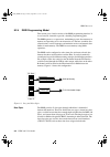
8-4 isdn and 16-bit audio dbri overview 8.2.4 dbri programming model this section gives a brief overview of the dbri programming interface. It is not, however, intended to provide a detailed programming guide. The dbri operates as a coprocessor, maintaining its own data structures in memory and oper...
Page 101
Isdn and 16-bit audio 8-5 dbri overview long pipes can be configured to pass data through transparently or to code or decode data as hdlc frames. The ccitt q921 protocol requires that protocol information is coded as hdlc formatted packets whereas payload data on the b channels does not require proc...
Page 102
8-6 isdn and 16-bit audio dbri overview time slots each of the dbrl's three serial interfaces (chi, nt and te) can have time slots defined for them. A time-slot descriptor (tsd) must be assigned to one end of the data pipe in order for data to enter or leave that end of the data pipe via a serial in...
Page 103: 8.2.5
Isdn and 16-bit audio 8-7 dbri overview fixed i/0 channels s and q channels are supported on the basic rate interfaces. They can be connected to short data pipes, the other ends of which are in fixed i/o mode. Commands set a value for s and q which is output repeatedly until changed. If an incoming ...
Page 104
8-8 isdn and 16-bit audio dbri overview reg0: status and control register bit 15 p – this bit is set by the host or by the dbri when reg8 (command pointer) is written. It is cleared by the dbri when a wait command is encountered on the command list. When the bit is set, the dbri begins executing com...
Page 105
Isdn and 16-bit audio 8-9 dbri overview bit 1 h – this bit is set and cleared by the host. Setting this bit halts all dma associated with the long data pipes (these can be delayed) but enables the dbri to continue execution of commands from the command queue. Any command which controls a data pipe (...
Page 106
8-10 isdn and 16-bit audio dbri overview reg2:parallel i/o register this register is associated with parallel i/o port (pio) operations. Three of the pio pins are used to control d/c, pdn and reset pins of the audio codec. The bits in this register are assigned as shown in table 10-6 (all other bits...
Page 107: 8.2.6
Isdn and 16-bit audio 8-11 dbri overview 8.2.6 dbri commands control of the dbri is mainly accomplished using commands. Table 8-2 lists the dbri command set. Command execution is started when a pointer to the first command is written into reg8. Each command is at least one word in length. The first ...
Page 108
8-12 isdn and 16-bit audio dbri overview • te – set te interface operating modes. • nt – set nt interface operating modes. • cdm – set chi operating modes. • pause – pause command execution to allow previous sdp commands to take effect. • cdp – reexamine transmit or receive descriptor pointer, to ex...
Page 109: 8.2.7
Isdn and 16-bit audio 8-13 dbri overview 8.2.7 data structures dbri instructions, descriptors and transmit and receive data buffers are stored in data structures in main memory. Instruction execution is initiated by loading a pointer to the first instruction into reg8. The dbri then continues by fet...
Page 110: 8.3
8-14 isdn and 16-bit audio audio codec 8.3 audio codec a crystal semiconductor corporation cs4215 multimedia audio coder-decoder (codec) provides the sparcbook 3 with stereo audio capabilities. It operates in conjunction with the dbri with which it is connected via a synchronous serial link. The dbr...
Page 111
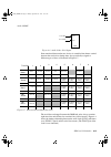
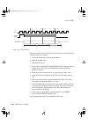
Isdn and 16-bit audio 8-15 audio codec data transferred between the two devices is assembled into frames carried between the tow devices during times slots specifically assigned to different types of data, as illustrated in figure 8-7. The serial data exchanged between the dbri and codec always cont...
Page 112
8-16 isdn and 16-bit audio audio codec the steps required to move the audio codec from data to control mode and then back again are as follows: 1. Lower the output level to maximum attenuation. 2. Mute the speaker output 3. Take the d/c pin low. 4. If the codec is timing master and the itsd bit in t...
Page 113: 8.3.2
Isdn and 16-bit audio 8-17 audio codec 11. Set the d/c line high to place the codec in data mode. The codec will execute an offset calibration cycle 12. Transmit or receive audio data. 8.3.2 control mode conrol information can be written to the audio codec, and status can be read while is is in the ...
Page 114
8-18 isdn and 16-bit audio audio codec data format register bits 5:3 data conversion frequency. The bits in this field are used to select the frequency have the following function: bit 2 stereo bit 0 = mono 1 = stereo bits 1:0 data format selection 00 = 16 bit law 01 = 8 bit µ law 10 = 8 bit a law 1...
Page 115
Isdn and 16-bit audio 8-19 audio codec 0 = fsync and sclk tri-sate 12 clock after d/c goes low 1 = fsync and sclk tri-sate immediately after d/c goes low bits 5:4 mck1:0 – clock source select 00 = sclk is master clock, 256 bits per frame. Bsel must be set to 2 and xclk must be set to 0. 01 = xtal 1 ...
Page 116: 8.3.3
8-20 isdn and 16-bit audio audio codec 8.3.3 data mode the data mode is used during conversions to pass digital audio data between the dbri and codec. The frame synchronization rate is equal to the value of the conversion frequency set by the by the dfr bits in the data fromat register. Each frames ...
Page 117
Isdn and 16-bit audio 8-21 audio codec bit 7 he – headphone output enable 0 = headphone disabled 1 = headphone enabled bit 6 le – line output enable 0 = line output disabled 1 = line output enabled bits 5:0 output attenuation for left channel. Lo(5) is msb. Lo(0) represents 1.5 db. 0 = no attenuatio...
Page 118
8-22 isdn and 16-bit audio audio codec intput setting bits 7:4 ma(3:0) – monitor path attenuation ma3 is the msb. Ma0 represents 6 db full gain is at least 22.5 db. Not used in mono modes. Bits 3:0 rg(3:0) – input gain for right channel rg3 is the msb. Lgo represents 1.5 db. Full gain is 22.5 db. 0 ...
Page 119: Modem
Modem 9 9 9 this chapter discusses the sparcbook 3’s internal modem. It uses a two-chip set comprising the r65c39 microcontroller unit (mcu) and rc144apl modem data pump (mdp). Connection to a telephone line is made via a data access arrangement (daa) which provides the required line isolation figur...
Page 120: 9.1
9-2 modem internal modem overview 9.1 internal modem overview the mcu provides the interface between the host system and dpl. It incorporates a processor core and a 16c450 uart-type parallel interface, and supports an enhanced at command set as well as fax class 2 commands. The mdp supports data and...
Page 121
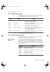
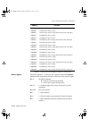
Modem 9-3 interface control the mcu registers are accessible at base address 0x0f0280000 and are shown in table 11-1. Bit 7 in the line control register is used as a pointer to either the transmit and receive buffers and the interrupt enable register, or to the divisor latch registers. Bit 7 must be...
Page 122: 9.3
9-4 modem modem registers 9.3 modem registers this section describes the more significant registers from the point of view of managing the flow of commands and data between main memory and the modem. 9.3.1 interrupt enable register this register contains interrupt control bits. Setting one of the in...
Page 123: 9.3.3
Modem 9-5 at command set 9.3.3 line status register the line status register contains information which allows the condition of the transmit and receive buffers to be monitored. Bit 7 reserved bit 6 transmitter empty this bit when set indicates that both the transmit buffer and the transmit shift re...
Page 124
9-6 modem at command set code description a go off-hook in answer mode a/ re-execute previous command at attention characters b bell/ccitt protocol d dial telephone number en command echo fn select line modulation hn switch hook control in identification nn automode o return to online p set pulse di...
Page 125
Modem 9-7 at command set with the exception of a/, all command lines begin with the attention characters “at” followed by one or more command characters, and are terminated with a return . Command lines may contain up to 56 characters, including a and t. All characters before the at string, and all ...
Page 126
9-8 modem at command set en echo command characters this controls whether the modem echoes command characters back to the host: n = 0 disable character echo n = 1 enable character echo fn select line modulation this selects line modulation: n = 0 auto dial mode n = 1 v.21 or bell 103 (according to b...
Page 127
Modem 9-9 at command set sn? Read s register this returns the contents of an s register n = s-register vn response format this command is used to select the format of response made by the modem to the host: n = 0 single digit response n = 1 extended response xn select extended response set &fn fetch...
Page 128
9-10 modem at command set *c remote configuration password this instructs the modem to store a password. By supplying a matching password, a remote modem may reconfigure the local modem. Supplied by a remote modem. *d display delayed numbers this causes the modem to send a list of delayed numbers an...
Page 129: 9.5
Modem 9-11 s registers 9.5 s registers the sparcbook modem provides a set of s registers which can be used to control the activity and configuration of the modem, and can be used to obtain status information. A set of default values (or profile) are loaded into these registers during system power-on...
Page 130
9-12 modem s registers register function s0 rings to auto-answer s1 incoming ring counter s2 escape character s3 carriage return character s4 line feed character s5 backspace character s6 dial tone wait time s7 wait time for remote carrier s8 pause time for dial delay modifier s9 carrier detect resp...
Page 131
Modem 9-13 s registers s3 carriage return character sets the command line and result code terminator character. Pertains to asynchronous operation only. Range: 0-127, ascii decimal, default: 13 (carriage return) s4 line feed character sets the character recognized as a line feed. Pertains to asynchr...
Page 132
9-14 modem s registers detection of answer tone if allowed by country restrictions. This timer also specifies the wait for silence time of the @ dial modifier in seconds. S7 is not associated with the w dial modifier. Range: 0-255 seconds, default: 50 s8 pause time for dial delay sets the time, in s...
Page 133
Modem 9-15 s registers s14 general bit mapped options indicates the status of command options. Default: 138 (8ah) (10001010b) bit 0 this bit is ignored bit 1 command echo (en) 0 = disabled (e0) 1 = enabled (e 1) (default) bit 2 quiet mode (qn) 0 = send result codes (q0) (default) 1 = do not send res...
Page 134
9-16 modem s registers 1 = enabled (&t7) bit 6 local analog loopback (lal) with self test 0 = disabled (default) 1 = enabled (&t8) bit 7 not used s17 reserved s18 test timer sets the length of time, in seconds, that the modem conducts a test (commanded by &tn) before returning to the command line. I...
Page 135
Modem 9-17 s registers s22 speaker/results bit mapped options indicates the status of command options. Default 117 (75h) (01110101b) bit 0,1 speaker volume (ln) 0 = (l0) 1 = low (l1) (default) 2 = medium (l2) 3 = high (l3) bit 2,3 speaker control (mn) 0 = disabled (m0) 1 = off on carrier (m1) (defau...
Page 136
9-18 modem s registers 0 = none (&g0) 1 = none (&g1) 2 = 1800 hz (&g2) (default) s24 sleep inactivity timer sets the length of time, in units of 10 seconds, that the modem will operate in normal mode with no detected telephone line dte line activity before entering low-power sleep mode. The timer is...
Page 137
Modem 9-19 s registers 0 = dial up line (&l0) (default) 1 = leased line (&l1) bit 4,5 internal clock select (&xn) 0 = internal clock (&x0) (default) 1 = external clock (&x1 ) 2 = slave clock (&x2) bit 6 ccitt/bell mode select (bn) 0 = ccitt mode (b0) (default) 1 = bell mode (b1) bit 7 reserved s28 b...
Page 138
9-20 modem s registers inoperative in synchronous mode. Range: 0-255 tenths of a second, default:0 (disabled) s31 bit mapped options default: 2 (00000010b) bit 0 reserved bit 1 controls auto line speed detection (nn) 0 = disabled (n0) 1 = enabled (n1) (default) bit 2, 3 controls error correction pro...
Page 139
Modem 9-21 s registers 4 = an mnp connection is attempted and if it fails, the modem disconnects 5 = an mnp connection is attempted and it fails, direct mode connection is established 6 = reserved 7 = an mnp connection is attempted and if it fails, normal mode connection is established (default) bit...
Page 140
9-22 modem s registers if s38 is set to 255, the modem does not time-out and continues to attempt to deliver data in the buffer until the connection is lost or the data is delivered. Range: 0-255 seconds, default: o s39 flow control default: 3 (00000011 b) bits 0-2 status of command options 0 = no f...
Page 141
Modem 9-23 s registers s41 general bit mapped options indicates the status of command options. Default: 3 (00000011b) bits 0 - 1 compression selection (%cn) 0 = disabled (%c0) 1 = mnp5 (%c1) 2 = v.42bis (%c2) 3 = mnp5 and v.42bis (%c2) (default) bit 2 auto retrain 0 = retrains disabled (%e0) (defaul...
Page 142
9-24 modem s registers default: 7 s48=0 disable negotiation; bypass the detection and negotiation phases; and proceed with lapm s48 = 7 enable negotiation (default) s48 = 128 disable negotiation; bypass the detection and negotiation phases; and proceed at once with the fallback action specified in s...
Page 143
Modem 9-25 s registers s82 = 3 expedited: modem sends a break immediately; data integrity is maintained both ahead of and after the break. S82 = 7 destructive: modem sends a break immediately; data being processed by each modem at the time of the break is destroyed. S82 = 128 in sequence: modem send...
Page 144
9-26 modem s registers s92 fax transmit level sets the transmit level, in dbm, for the fax mode. In some countries, this cannot be changed and there are checks to prevent transmit level change. Range: 0 to -15 dbm, default: 10 s95 extended result code the bits in this register can be set to override...
Page 145: 9.6
Modem 9-27 class 2 fax command set 9.6 class 2 fax command set the sparcbook internal modem is able to execute extended class 2 fax commands, summarized in table 9-4. These commands must be preceded by the at characters, and may be terminated with a semicolon (;) or return . Command function service...
Page 146
9-28 modem class 2 fax command set s3gx_trmbook page 28 friday, september 19, 1997 11:39 am.
Page 147: Parallel Interface
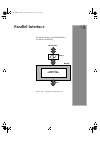
Parallel interface 1 1 1 0 0 0 the parallel interface on the sparcbook is provided by the macio. Figure 10-1 parallel port architecture parallel port interface / dma macio buffers sbus parallel port s3gx_trmbook page 1 friday, september 19, 1997 11:39 am.
Page 148: 10.1
10-2 parallel interface parallel port overview 10.1 parallel port overview the parallel port of the macio comprises four 8-bit port registers, three 16-bit configuration registers and a 64 byte fifo. Parallel communications can be carried out using programmed i/o or dma operations; the macio’s inter...
Page 149: 10.2
Parallel interface 10-3 parallel port control registers sequence of dma transfers of equal size from different addresses; only the next address register need be updated and the dma controller will simply load its new contents and the existing contents of the next byte counter. 10.2 parallel port con...
Page 150
10-4 parallel interface parallel port control registers bit 25 dma on (read-only) – when set, indicates that dma transfers are not disabled due to any hardware or software condition. Bit 24 enable next (r/w) – when set enables dma chaining, and autoloading of next registers. Bit 23 terminal count in...
Page 151: Display Interface
Display interface 1 1 1 1 1 1 this chapter discusses the sparcbook 3’s display interface. The display interface drives the built-in lcd flat panel display and is able to drive an an external crt display with resolutions of up to 1600 x 1200 pixels. Sparcbook 3 is able to display simultaneously in th...
Page 152: 11.1
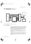
11-2 display interface display interface overview 11.1 display interface overview 11.1.1 architecture the display interface, illustrated in figure 11-1, is based around two major components, the weitek power 9100 user interface controller and an ibm rgb528 palette dac (ramdac). These provide advance...
Page 153
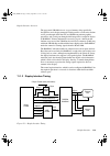
Display interface 11-3 display interface overview the page-mode vram device is a type of memory chip specifically designed for use in display memories which provides a read-write random access port through which the cpu and p9100 can perform graphics operations, and a serial port through which image...
Page 154: 11.1.3 Lcd Power
11-4 display interface display interface overview pixel clocks the ramdac incorporates a programmable pixel clock generator, which allows the pixel clock to be programmed to suit a large range of display formats. In the sparcbook 3 application, the ramdac generates a master pixel clock controlled by...
Page 155: 11.2
Display interface 11-5 power 9100 user interface controller 11.2 power 9100 user interface controller the weitek power 9100 user interface controller is an accelerated 2-d graphics processor which supports draw, fill, and bit block-transfer operations at the full speed of the page-mode vram employed...
Page 156: 11.2.1 Parameter Engine
11-6 display interface power 9100 user interface controller 11.2.1 parameter engine the parameter engine prepares drawing operations for the drawing engine; its function is to take input coordinates from the host and convert them to a form usable by the drawing engine. The input parameters include t...
Page 157: 11.2.4 Svga Unit
Display interface 11-7 power 9100 user interface controller non-interleaved vram modes. These registers are initialized during system startup and but can be reprogrammed discretely via a user interface provided by the nce display panel. 11.2.4 svga unit the power 9100 contains an svga unit which is ...
Page 158
11-8 display interface power 9100 user interface controller status and control registers and commands the power 9100 contains a number of registers which are used to control device operations. They are used, for example, to enable and handle interrupts, to control parameter and drawing engine operat...
Page 159
Display interface 11-9 power 9100 user interface controller note due to the behavior of the weikek power 9100 chip, writes to any register group must be preceded by a read from the framebuffer with address bits 14:07 matching the register group’s offset. Further accesses to registers within the same...
Page 160
11-10 display interface power 9100 user interface controller bit 25 reserved bit 24 drive load 2 0 = normal drive load 1 = double drive load bit 23 clocking – should be zero bits 22:20 shift control 0 bits 19:17 shift control 1 bits 16:14 shift control 2 the four shift control fields are used to def...
Page 161
Display interface 11-11 power 9100 user interface controller bits 8:3 reserved bits 2:0 p9100 version interrupt register this register records events that have triggered an interrupt. A bit when it is asserted to indicate the cause of interrupt stays asserted until cleared by a host write. Each bit ...
Page 162
11-12 display interface power 9100 user interface controller 0 = disable pick interrupts 1 = enable pick interrupts bits 1:0 drawing engine idle 0 = disable drawing engine idle interrupt 1 = enable drawing engine idle interrupt alternate read and alternate write bank registers these two registers sp...
Page 163
Display interface 11-13 power 9100 user interface controller screen repaint timing control register 1 the bits in this register are assigned as follows (required settings are shown in bold type): bits 31:11 reserved bits 10:9 sraddr increment size 00 = 256 01 = 512 10 = 1024 bit 8 vsync source 0 = e...
Page 164
11-14 display interface power 9100 user interface controller bit 7 hsync source 0 = external 1 = internal bit 6 reserved - must be set to 0 bit 5 enable video 0 = blanks asserted, hsync and vsync are disabled 1= normal operation bit 4 screen repaint mode 0 = normal 1 = restricted bit 3 buffer for di...
Page 165
Display interface 11-15 power 9100 user interface controller 11.2.8 vram control registers the vram control registers specify the timing and chip configuration of the p9100 vram interface. These are summarized below: 11.2.9 parameter engine registers the parameter engine registers include the device...
Page 166
11-16 display interface power 9100 user interface controller status register the status register is a 32-bit read-only register located at 0x38002000 which provides information about the current state of the drawing engine. Bit 31 quad/blit command 0 = ready for a quad or blit operation 1 = do not s...
Page 167
Display interface 11-17 power 9100 user interface controller bit 4 1 = quad exception, operation must be done in software bit 3 1 = requested quad is concave bit 2 1= source coordinates for quad draw entirely outside clipping window bit 1 1= source coordinates for quad draw entirely inside clipping ...
Page 168
11-18 display interface power 9100 user interface controller 11.2.10 drawing engine registers the drawing engine registers control pixel processing. They are used define foreground and background colors, plane masking, pattern and pattern origins, pixel drawing window limits, and raster operation pa...
Page 169
Display interface 11-19 power 9100 user interface controller draw mode register the bits in the draw mode register are assigned as follows: bits 31:04 reserved (contain zeroes) bits 3:2 pick write enable 0 = suppress any writes outside of the window 1 = suppress all writes; set the picked bit in the...
Page 170: 11.3
11-20 display interface direct frame buffer access bits 15:13 reserved (contains zeroes) bits 12:00 minimum or maximum y values 11.2.11 ramdac register accesses accesses to the ramdac’s internal registers are made through locations within the power 9100’s address space, see section 11.4.1, “ramdac h...
Page 171: 11.4
Display interface 11-21 ramdac sizes of display: a 640x480 pixel display using 8 bits per pixel; and a 1024 x 900 display using 16 bits per pixel. The framebuffer is considered in the illustration as a rectangular area with a horizontal dimension equivalent to the horizontal resolution of the displa...
Page 172
11-22 display interface ramdac 11.4.1 ramdac host interface the ramdac host interface is mapped through the ramdac space of the p9100 at 0x38000200. In response to addresses in the ramdac region, the power 9100 generates register select signals to select the target register. The ramdac provides a by...
Page 173
Display interface 11-23 ramdac register at 0x38000220 and the value 0x00 would be written into the index high register at 0x38000228, and then the read enable register could be accessed at 0x38000230. The column ‘contents’ shows the values which must be used for the sparcbook 3 to operate correctly....
Page 174
11-24 display interface ramdac 000f buffer a/b select 12 0010 pixel pll control 1 0x2 13 0011 pixel pll control 2 0x00 0012 - 0013 reserved 14 0014 fixed pixel pll reference divider 0x05 (manditory for 10 mhz) 16 0015 system pll reference divider 0x05 17 0016 system pll vco divider 0x63 (for 50 mhz ...
Page 175
Display interface 11-25 ramdac 0035 cursor x hotspot 0036 cursor y hotspot 0037 - 003f reserved 0040 cursor color 1 red 0041 cursor color 1 green 0042 cursor color 1 blue 0043 cursor color 2 red 0044 cursor color 2 green 0045 cursor color 2 blue 0046 cursor color 3 red 0047 cursor color 3 green 0048...
Page 176
11-26 display interface ramdac a brief description is given below of the register accessed during initialization. For a full description, please refer to the manufacturer’s data sheet, see appendix a, “further information”. Miscellaneous control 1 – index 0x0070 this register must contain the value ...
Page 177
Display interface 11-27 ramdac synchronization control – index 0x0003 this register controls how the ramdac uses the sync input signals and how it drives the sync outputs. This register must contain 0x00. To operate correclty within its hardware environment. Horizontal sync position – index 0x0004 t...
Page 178
11-28 display interface ramdac 11.4.3 color palette accesses the ramdac contains three 256 x 8 bit color lookup tables (palettes) which are accessed as a single 256 x 24 bit palette via an internal control mechanism. Before reading from the palette, the palette address (read mode) register must be w...
Page 179: 11.4.4 Pixel Formats
Display interface 11-29 ramdac palette location in a single transfer. This mechanism allows successive byte writes to the palette data location to step through the 256 palette entries without the need to supply a new address for each access. The address register is reset to zero following an access ...
Page 180
11-30 display interface ramdac s3gx_trmbook page 30 friday, september 19, 1997 11:39 am.
Page 181: Microcontroller Subsystem
Microcontroller subsystem 1 1 1 2 2 2 this chapter decribes the microcontroller subsystem which provides low-level system management for the sparcbook 3. System management includes the following: • monitoring and controlling initial system power-up • handling keyboard and pointing stick input • moni...
Page 182: 12.1
12-2 microcontroller subsystem microcontroller subsystem overview 12.1 microcontroller subsystem overview the architecture of the microcontroller subsystem is illustrated in figure 12-1. The illustration above shows scope of the microcontroller subsystem’s role. The microcontroller incorporates on-c...
Page 183: 12.1.1 Normal Operation
Microcontroller subsystem 12-3 microcontroller subsystem overview assigning low level activites activities to a dedicated microcontroller in this way releives the main cpu of the burden of trivial activities, ensuring that it is employed effeciently running applications. The host cpu and microcontro...
Page 184: 12.1.4 Pointing Stick
12-4 microcontroller subsystem microcontroller subsystem overview 12.1.2 internal keyboard scanning the microcontroller address bus signals are driven out to the internal keyboard drive lines and depressed keys are sensed via the data bus. The microcontroller implements debounce and key repeat contr...
Page 185: 12.1.7 Lcd Status Display
Microcontroller subsystem 12-5 microcontroller subsystem overview 12.1.7 lcd status display the status screen is managed by the microcontroller. The display can be programmed for continuous loop or static message display. A stringcode table defines characters and text strings to be used for any mess...
Page 186: 12.2
12-6 microcontroller subsystem command set 12.2 command set the microcontroller command set is organized into several functional groups. The command structure is the same for all groups. 12.2.1 command synchronization the administartion of the host-microcontroller link must be single threaded; only ...
Page 187
Microcontroller subsystem 12-7 command set 0x0a read power-on seconds ack + 4bytes this command returns the total number of seconds that the unit has been powered-on during its life. This value is held in eeprom as a four byte value which are returned in order msb ... Lsb. This value will overflow i...
Page 188
12-8 microcontroller subsystem command set 0x0d read real time clock ack + 7 bytes the microcontroller reads the values from the rtc and returns them in the order: seconds, minutes, hour, day, date monthe, year. This command will fail (return nack) if the rtc reports an internal error. 0x0e read ext...
Page 189
Microcontroller subsystem 12-9 command set 0x12 read user configuration area and address ack + 2 bytes the user configuration area of the eeprom is used to store long-lived system configuration information. This area can be read and written by using the read and write eeprom commands, provided that ...
Page 190
12-10 microcontroller subsystem command set 0x1c read internal keyboard layout ack + 2 bytes this command returns the keyboard type (first byte) and layout information (second byte) for the unit's internal keyboard. This value is recorded in eeprom, but defaults to sun type 5 us layout if the eeprom...
Page 191
Microcontroller subsystem 12-11 command set 12.2.3 read/write/modify commands these commands are used to read or modify the byte attribute addressed. Each command uses the same form, where the value written to the attribute is given by: new_attribute = (old_attribute and mask) eor value the old attr...
Page 192
12-12 microcontroller subsystem command set 0x23 speaker volume mask ack + 1 byte the volume is controlled via a digital potentiometer which is varied with this command. Values in the range 0-255 (dec) are acceptable when setting this parameter. The value is stored in eeprom and is used to determine...
Page 193
Microcontroller subsystem 12-13 command set 0x2e control diagnostic mode mask ack + ((mark_space_ratio and mask) eor value) this command is used to control various features used during diagnostic test of the system. By setting the appropriate bit in this simulated "port", a diagnostic feature is act...
Page 194
12-14 microcontroller subsystem command set 12.2.4 commands returning no status the following commands are provided to simplify the use of the micromcontroller by system software, particularly form interrupt routines. No status is returned for these commands and in many cases the commands do not req...
Page 195
Microcontroller subsystem 12-15 command set 12.2.5 block transfer commands this gorup of commands handle transfers of arbitrary amounts of data, up to a maximum of 255 bytes, between the cpu and microcontroller. A length parameter of zero transfers no data. Attenpts to transfer excess data results i...
Page 196: 12.2.6 Generic Commands
12-16 microcontroller subsystem command set 12.2.6 generic commands this group of commands perform related functions and are of variable length. Opcode command argument returned function 0x50 define key combination entry (sequence and combination_length ) ack the built-in keyboard features an 86-key...
Page 197
Microcontroller subsystem 12-17 command set 12.2.7 generic commands with optional status 0x52 define status screen display length bytes and puase descriptor> ack the lcd status screen can be set up to display a continuous loop of messages separated by definable pauses, or to display a single message...
Page 198
12-18 microcontroller subsystem command set 12.2.8 administration commands opcode command arguments returned function 0x70 set user password length ack the supplied user password is encrypted and stored in eeprom. The microcontroller fails attempts to use this command if a password not been supplied...
Page 199: Further Information
Further information a a a this appendix provides a list of publications or websites to which you can refer for further information about components used in the sparcbook 3. S3gx_trmbook page 1 friday, september 19, 1997 11:39 am.
Page 200
A-2 further information device facility provided contact stsx1012 microsparc ii cpu, sbus controller, memory controller http://www.Sun.Com/sparc turbosparc cpu, sbus controller, memory controller (s3tx only) turbosparc microprocessor user’s guide revision 1.0, october 1996 fujitsu microelectronic in...
Page 201: Connector Information
Connector information b b b this appendix provides a pinouts for the connectors used the sparcbook 3. S3gx_trmbook page 1 friday, september 19, 1997 11:39 am.
Page 202: B.1
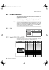
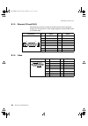
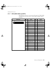
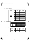
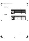
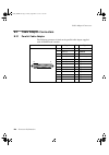
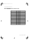
B-2 connector information i/o panel connectors b.1 i/o panel connectors this chapter provides details of the connector-pin signal assignments for the interfaces on the i/o panel. Sparcbook 3 systems are supplied with cable adapters, where required, so that interfaces appear on the appropriate indust...
Page 203: B.1.3
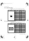
Connector information b-3 i/o panel connectors b.1.3 parallel (s3 and s3lc) the following connector is fitted on the i/o panel of the s3 and s3lc models. B.1.4 ethernet (s3xp, s3gx and s3tx) the following connector is fitted on the i/o panel of the s3xp, s3gx and s3tx. It is the lower connector of a...
Page 204: B.1.5
B-4 connector information i/o panel connectors b.1.5 ethernet (s3 and s3lc) the following connector is fitted on the i/o panel of the s3 and s3lc models. It is also present on a cable adapter supplied with the s3xp, s3gx and s3tx models. B.1.6 video a.Protected internally by a self-resetting fuse co...
Page 205: B.1.7
Connector information b-5 i/o panel connectors b.1.7 scsi (s3xp, s3gx and s3tx) the following connector is fitted on the i/o panel of s3 xp, s3gx and s3tx and is present on the a cable adapter supplied with s3 and s3lc connector pin signal pin signal 1 signal ground 26 scsi d (0) 2 signal ground 27 ...
Page 206: B.1.8
B-6 connector information i/o panel connectors b.1.8 scsi (s3 and s3lc) the following connector is fitted to the i/o panel of s3 and s3lc models. B.1.9 keyboard/mouse b.1.10 serial (x2) connector pin signal pin signal 1 not connected 16 scsi d(6) 2 scsi d(0) 17 signal ground 3 signal ground 18 scsi ...
Page 207: B.1.11 Isdn
Connector information b-7 i/o panel connectors b.1.11 isdn the following connector is not present on the s3lc. Modem connector pin signal pin signal 1 not connected 5 te in– 2 not connected 6 te out– 3 te out+ 7 not connected 4 te in+ 8 not connected 1 6 2 3 4 5 7 8 connector pin signal pin signal 1...
Page 208: B.2
B-8 connector information cable adapter connectors b.2 cable adapter connectors b.2.1 parallel cable adapter the following connector is fitted on the parallel cable adapter supplied with all sparcbook 3 models. Connector pin signal pin signal 1 /strobe 14 /autofeed 2 data (0) 15 /error 3 data (l) 16...
Page 209: B.3
Connector information b-9 removable hard drive scsi connector b.3 removable hard drive scsi connector signal pin pin signal motorvcc 1 21 motorvcc motorgnd 2 22 motorgnd /scsiio 3 23 gnd /scsicd 4 24 scsid(7) /scsisel 5 25 gnd /scsireq 6 26 scsid(6) /scsirst 7 27 gnd /scsimsg 8 28 scsid(5) /scsiiack...
Page 210
B-10 connector information removable hard drive scsi connector s3gx_trmbook page 10 friday, september 19, 1997 11:39 am.
Page 211: Numerics
I -i numerics 16-bit audio interface 8-1 a address map power 9100 registers 11-8 slavio 3-4 ts102 7-4 address map, system 3-2 address translation 2-11 architecture display interface 11-2 ebus 1-8 ethernet interface 6-1 internal modem 9-1 isdn and audio interface 8-1 microcontroller subsystem 12-2 mi...
Page 212
Index-ii d data mode, audio codec 8-20 dbri command summary 8-12 commands 8-11 internal registers 8-7 programming model 8-4 dbri data structures 8-13 dbri sbus interface 8-3 dc-in connector b-2 definitions data entities xi logic states xi descriptor management, ethernet 6-2 diagnostic message regist...
Page 213
Index-iii ramdac 11-23 instruction set overview 2-3 integer unit 2-5, 2-6 control registers 2-6 cycles per instruction 2-4 window registers 2-6 integer unit, microsparc 2-3 internal keyboard scanning 12-4 internal modem 9-1, 9-27 architecture 9-1 area of approval 9-2 at command set 9-5 interface con...
Page 214
Index-iv network interface architecture 6-1 note on p9100 register access 11-9 note on ramdac access delays 11-22 note on ramdac address autoincrement 11-23 p page table pointer 2-11 parallel connector b-5 parallel interface 10-1 parallel port 1-11 architecture 10-1 dma operations 10-2 parallel port...
Page 215
Index-v connecting devices 5-2 scsi controller 1-10, 5-1 configuration registers 5-6 dma registers 5-7 dma support 5-7 fifo/flags register 5-6 interrupt status register 5-5 interrupts 5-7 select/reconnect register 5-6 sequence step register 5-6 status register 5-5 synchronous transfer period registe...
Page 216
Index-vi s3gx_trmbook page vi friday, september 19, 1997 11:39 am.


