- DL manuals
- Xilinx
- Motherboard
- Spartan-6 FPGA Series
- Design And Pin Planning Manual
Xilinx Spartan-6 FPGA Series Design And Pin Planning Manual
Summary of Spartan-6 FPGA Series
Page 1
Spartan-6 fpga pcb design and pin planning guide ug393 (v1.1) april 29, 2010
Page 2: Revision History
Spartan-6 fpga pcb design and pin planning www.Xilinx.Com ug393 (v1.1) april 29, 2010 xilinx is disclosing this user guide, manual, release note, and/or specification (the "documentation") to you solely for use in the development of designs to operate with xilinx hardware devices. You may not reprod...
Page 3: Table of Contents
Spartan-6 fpga pcb design and pin planning www.Xilinx.Com 3 ug393 (v1.1) april 29, 2010 revision history . . . . . . . . . . . . . . . . . . . . . . . . . . . . . . . . . . . . . . . . . . . . . . . . . . . . . . . . . . . . . 2 preface: about this guide guide contents . . . . . . . . . . . . . . . ...
Page 4
4 www.Xilinx.Com spartan-6 fpga pcb design and pin planning ug393 (v1.1) april 29, 2010 simulation methods . . . . . . . . . . . . . . . . . . . . . . . . . . . . . . . . . . . . . . . . . . . . . . . . . . . . . . . . 32 pds measurements . . . . . . . . . . . . . . . . . . . . . . . . . . . . . . ....
Page 5
Spartan-6 fpga pcb design and pin planning www.Xilinx.Com 5 ug393 (v1.1) april 29, 2010 chapter 6: i/o pin and clock planning configuration modes . . . . . . . . . . . . . . . . . . . . . . . . . . . . . . . . . . . . . . . . . . . . . . . . . . . . . . . 61 configuration pin planning considerations...
Page 6
6 www.Xilinx.Com spartan-6 fpga pcb design and pin planning ug393 (v1.1) april 29, 2010
Page 7: About This Guide
Spartan-6 fpga pcb design and pin planning www.Xilinx.Com 7 ug393 (v1.1) april 29, 2010 preface about this guide this guide provides information on pcb design for spartan®-6 devices, with a focus on strategies for making design decisions at the pcb and interface level. Guide contents this guide cont...
Page 8
8 www.Xilinx.Com spartan-6 fpga pcb design and pin planning ug393 (v1.1) april 29, 2010 preface: about this guide this all-encompassing configuration guide includes chapters on configuration interfaces (serial and parallel), multi-bitstream management, bitstream encryption, boundary-scan and jtag co...
Page 9: Pcb Technology Basics
Spartan-6 fpga pcb design and pin planning www.Xilinx.Com 9 ug393 (v1.1) april 29, 2010 chapter 1 pcb technology basics printed circuit boards (pcbs) are electrical systems, with electrical properties as complicated as the discrete components and devices mounted to them. The pcb designer has complet...
Page 10
10 www.Xilinx.Com spartan-6 fpga pcb design and pin planning ug393 (v1.1) april 29, 2010 chapter 1: pcb technology basics transmission of signals along traces because they are the return current transmission medium. Vias a via is a piece of metal making an electrical connection between two or more p...
Page 11: Transmission Lines
Spartan-6 fpga pcb design and pin planning www.Xilinx.Com 11 ug393 (v1.1) april 29, 2010 transmission lines package pin or ball pitch (1.0 mm for fg packages) defines the land pad layout. The minimum surface feature sizes of current pcb technology define the via arrangement in the area under the dev...
Page 12: Return Currents
12 www.Xilinx.Com spartan-6 fpga pcb design and pin planning ug393 (v1.1) april 29, 2010 chapter 1: pcb technology basics dielectric constant of the material in the space around the signal trace and between the signal trace and the reference plane. The dielectric constant of the material in the vici...
Page 13: Power Distribution System
Spartan-6 fpga pcb design and pin planning www.Xilinx.Com 13 ug393 (v1.1) april 29, 2010 chapter 2 power distribution system this chapter documents the power distribution system (pds) for spartan®-6 fpgas, including decoupling capacitor selection, placement, and pcb geometries. A simple decoupling m...
Page 14
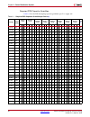
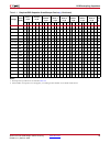
14 www.Xilinx.Com spartan-6 fpga pcb design and pin planning ug393 (v1.1) april 29, 2010 chapter 2: power distribution system required pcb capacitor quantities table 2-1 lists the pcb decoupling capacitor guidelines per v cc supply rail. Table 2-1: required pcb capacitor quantities per device (1) pa...
Page 15
Spartan-6 fpga pcb design and pin planning www.Xilinx.Com 15 ug393 (v1.1) april 29, 2010 pcb decoupling capacitors fg(g)484 lx75 3 10 20 1 4 9 1 3 5 1 3 6 1 4 7 1 4 6 89 fg(g)484 lx75t 3 10 20 1 4 7 1 2 3 1 3 6 1 3 6 1 3 6 81 fg(g)484 lx100 4 13 27 1 4 8 1 3 5 1 3 6 1 4 6 1 4 6 98 fg(g)484 lx100t 4 ...
Page 16
16 www.Xilinx.Com spartan-6 fpga pcb design and pin planning ug393 (v1.1) april 29, 2010 chapter 2: power distribution system capacitor specifications the electrical characteristics of the capacitors in table 2-1 are described in this section. Characteristics of the pcb bulk and high-frequency capac...
Page 17
Spartan-6 fpga pcb design and pin planning www.Xilinx.Com 17 ug393 (v1.1) april 29, 2010 pcb decoupling capacitors capacitor consolidation rules sometimes a number of i/o banks are powered from the same voltage (e.G., 1.8v) and the recommended guidelines call for multiple bulk capacitors. This is al...
Page 18
18 www.Xilinx.Com spartan-6 fpga pcb design and pin planning ug393 (v1.1) april 29, 2010 chapter 2: power distribution system 0805 ceramic capacitor the 4.7 µf 0805 capacitor covers the middle frequency range. Placement has some impact on its performance. The capacitor should be placed as close as p...
Page 19
Spartan-6 fpga pcb design and pin planning www.Xilinx.Com 19 ug393 (v1.1) april 29, 2010 pcb decoupling capacitors 0402 ceramic capacitor the 0.47 µf 0402 capacitor covers the high-middle frequency range. Placement and mounting are critical for these capacitors. The capacitor should be mounted as cl...
Page 20: Basic Pds Principles
20 www.Xilinx.Com spartan-6 fpga pcb design and pin planning ug393 (v1.1) april 29, 2010 chapter 2: power distribution system basic pds principles the purpose of the pds and the properties of its components are discussed in this section. The important aspects of capacitor placement, capacitor mounti...
Page 21
Spartan-6 fpga pcb design and pin planning www.Xilinx.Com 21 ug393 (v1.1) april 29, 2010 basic pds principles because the voltage level of v cc for a device is fixed, changing power demands are manifested as changing current demand. The pds must accommodate these variances of current draw with as li...
Page 22
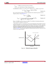
22 www.Xilinx.Com spartan-6 fpga pcb design and pin planning ug393 (v1.1) april 29, 2010 chapter 2: power distribution system figure 2-4 shows a simplified pds circuit with all reactive components represented by a frequency-dependent resistor. Role of inductance inductance is the property of the cap...
Page 23
Spartan-6 fpga pcb design and pin planning www.Xilinx.Com 23 ug393 (v1.1) april 29, 2010 basic pds principles requirements for choosing decoupling capacitors: • for a specific capacitance value, choose the smallest package available. - or - • for a specific package size (essentially a fixed inductan...
Page 24
24 www.Xilinx.Com spartan-6 fpga pcb design and pin planning ug393 (v1.1) april 29, 2010 chapter 2: power distribution system as capacitive value is increased, the capacitive curve moves down and left. As parasitic inductance is decreased, the inductive curve moves down and right. Because parasitic ...
Page 25
Spartan-6 fpga pcb design and pin planning www.Xilinx.Com 25 ug393 (v1.1) april 29, 2010 basic pds principles a connecting trace length has a large impact on the mounting’s parasitic inductance and if used, should be as short and wide as possible. When possible, a connecting trace should not be used...
Page 26
26 www.Xilinx.Com spartan-6 fpga pcb design and pin planning ug393 (v1.1) april 29, 2010 chapter 2: power distribution system spreading inductance acts like any other inductance and resists changes to the amount of current in a power plane (the conductor). The inductance retards the capacitor’s abil...
Page 27
Spartan-6 fpga pcb design and pin planning www.Xilinx.Com 27 ug393 (v1.1) april 29, 2010 basic pds principles the two opposing paths reduces the loop’s total inductance. Therefore, when given a choice, v cc and gnd vias should be as close together as possible. The via field under an fpga has many v ...
Page 28
28 www.Xilinx.Com spartan-6 fpga pcb design and pin planning ug393 (v1.1) april 29, 2010 chapter 2: power distribution system currents and are placed high in the stackup, while low priority pairs carry lower transient currents (or can tolerate more noise) and are placed in the lower part of the stac...
Page 29
Spartan-6 fpga pcb design and pin planning www.Xilinx.Com 29 ug393 (v1.1) april 29, 2010 basic pds principles f rself = 53 mhz (capacitor data sheet parameter) l mount = 0.8 nh (based on pcb mounting geometry) to determine the effective in-system parasitic inductance (l is ), add the via parasitics:...
Page 30
30 www.Xilinx.Com spartan-6 fpga pcb design and pin planning ug393 (v1.1) april 29, 2010 chapter 2: power distribution system capacitor anti-resonance one problem associated with combinations of capacitors in a pds of an fpga is anti- resonant spikes in the pds aggregate impedance. The cause for the...
Page 31
Spartan-6 fpga pcb design and pin planning www.Xilinx.Com 31 ug393 (v1.1) april 29, 2010 basic pds principles a finite time delay ( equation 2-6 ) occurs between the start of the disturbance at the fpga power pins and the point when the capacitor senses the disturbance. Equation 2-6 the dielectric i...
Page 32: Simulation Methods
32 www.Xilinx.Com spartan-6 fpga pcb design and pin planning ug393 (v1.1) april 29, 2010 chapter 2: power distribution system unconnected v cco pins in some cases, one or more i/o banks in an fpga are not used (for example, when an fpga has far more i/o pins than the design requires). In these cases...
Page 33: Pds Measurements
Spartan-6 fpga pcb design and pin planning www.Xilinx.Com 33 ug393 (v1.1) april 29, 2010 pds measurements pds measurements measurements can be used to determine whether a pds is adequate. Pds noise measurements are a unique task, and many specialized techniques have been developed. This section desc...
Page 34
34 www.Xilinx.Com spartan-6 fpga pcb design and pin planning ug393 (v1.1) april 29, 2010 chapter 2: power distribution system figure 2-9 shows an averaged noise measurement taken at the v cco pins of a sample design. In this case, the trigger was the clock for an i/o bus interface sending a 1-0-1-0 ...
Page 35
Spartan-6 fpga pcb design and pin planning www.Xilinx.Com 35 ug393 (v1.1) april 29, 2010 pds measurements figure 2-10 shows an infinite persistence noise measurement of the same design with a wider variety of i/o activity. Because the infinite persistence measurement catches all noise events over a ...
Page 36
36 www.Xilinx.Com spartan-6 fpga pcb design and pin planning ug393 (v1.1) april 29, 2010 chapter 2: power distribution system excessive noise at a certain frequency indicates a frequency where the pds impedance is too high for the device’s transient current demands. Using this information, the desig...
Page 37: Troubleshooting
Spartan-6 fpga pcb design and pin planning www.Xilinx.Com 37 ug393 (v1.1) april 29, 2010 troubleshooting optimum decoupling network design if a highly optimized pds is needed, measurements and simulations of a prototype system can inform the pds design. Using knowledge of the noise spectrum generate...
Page 38
38 www.Xilinx.Com spartan-6 fpga pcb design and pin planning ug393 (v1.1) april 29, 2010 chapter 2: power distribution system millimeters from the capacitor solder lands on the board, the current loop area is greater than necessary (see figure 2-1a ). To reduce the current loop area, vias should be ...
Page 39: Selectio Signaling
Spartan-6 fpga pcb design and pin planning www.Xilinx.Com 39 ug393 (v1.1) april 29, 2010 chapter 3 selectio signaling the spartan-6 fpga selectio resources are the general-purpose i/o and its various settings. With numerous i/o standards and hundreds of variants within these standards, these selecti...
Page 40: Single-Ended Signaling
40 www.Xilinx.Com spartan-6 fpga pcb design and pin planning ug393 (v1.1) april 29, 2010 chapter 3: selectio signaling is higher than the voltage of the p signal, the state is considered low. Typically the p and n signals have similar swing, and have a common-mode voltage above gnd (although this is...
Page 41: Pcb Materials and Traces
Spartan-6 fpga pcb design and pin planning www.Xilinx.Com 41 ug393 (v1.1) april 29, 2010 chapter 4 pcb materials and traces the choice of transmission media, whether pcb materials or cable type, can have a large impact on system performance. Although any transmission medium is lossy at gigahertz fre...
Page 42
42 www.Xilinx.Com spartan-6 fpga pcb design and pin planning ug393 (v1.1) april 29, 2010 chapter 4: pcb materials and traces loss tangent loss tangent is a measure of how much electromagnetic energy is lost to the dielectric as it propagates down a transmission line. A lower loss tangent allows more...
Page 43: Traces
Spartan-6 fpga pcb design and pin planning www.Xilinx.Com 43 ug393 (v1.1) april 29, 2010 traces traces trace geometry for any trace, its characteristic impedance is dependent on its stackup geometry as well as the trace geometry. In the case of differential traces, the inductive and capacitive coupl...
Page 44
44 www.Xilinx.Com spartan-6 fpga pcb design and pin planning ug393 (v1.1) april 29, 2010 chapter 4: pcb materials and traces a good pcb manufacturer understands controlled impedance and allows fine adjustments for line widths to produce a z 0o of 50 Ω . The pcb manufacturer also provides the paramet...
Page 45
Spartan-6 fpga pcb design and pin planning www.Xilinx.Com 45 ug393 (v1.1) april 29, 2010 traces trace routing high-speed serial differential traces are routed with the highest priority to ensure that the optimal path is available to these critical traces. This reduces the need for bends and vias and...
Page 46: Cable
46 www.Xilinx.Com spartan-6 fpga pcb design and pin planning ug393 (v1.1) april 29, 2010 chapter 4: pcb materials and traces simulating lossy transmission lines due to the different modeling implementations used by various circuit simulators (frequency-domain versus time-domain techniques), it is im...
Page 47: Signals
Spartan-6 fpga pcb design and pin planning www.Xilinx.Com 47 ug393 (v1.1) april 29, 2010 chapter 5 design of transitions for high-speed signals each transition in the channel must be designed to minimize any negative impact on the link performance. This chapter addresses the interface at either end ...
Page 48
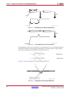
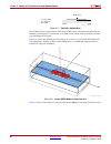
48 www.Xilinx.Com spartan-6 fpga pcb design and pin planning ug393 (v1.1) april 29, 2010 chapter 5: design of transitions for high-speed signals the magnitude of this excess capacitance (c) or inductance (l) can also be extracted from the tdr waveform by integrating the normalized area of the transi...
Page 49: Bga Package
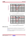
Spartan-6 fpga pcb design and pin planning www.Xilinx.Com 49 ug393 (v1.1) april 29, 2010 bga package the results using these equations are not sensitive to rise time variation and are valid for simulated tdr measurements provided that the leading and trailing transmission lines are very close to 50 ...
Page 50
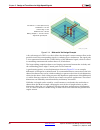
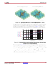
50 www.Xilinx.Com spartan-6 fpga pcb design and pin planning ug393 (v1.1) april 29, 2010 chapter 5: design of transitions for high-speed signals the 2d field-solver example shows that close to 50 Ω can be achieved if the ground plane under the pad footprint is cleared out. A 3d field solver is then ...
Page 51
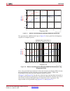
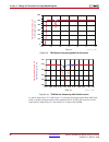
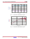
Spartan-6 fpga pcb design and pin planning www.Xilinx.Com 51 ug393 (v1.1) april 29, 2010 smt pads the approximately –40 db/decade slope in figure 5-8 shows good fit to the frequency response of a lumped capacitor. Next, using simulated measurements on the same transition modeled in hfss, the time- d...
Page 52
52 www.Xilinx.Com spartan-6 fpga pcb design and pin planning ug393 (v1.1) april 29, 2010 chapter 5: design of transitions for high-speed signals as shown from figure 5-11 and figure 5-12 , clearing the ground plane under smt pads yields a significant improvement in the performance of an smt pad tran...
Page 53: Differential Vias
Spartan-6 fpga pcb design and pin planning www.Xilinx.Com 53 ug393 (v1.1) april 29, 2010 differential vias differential vias the most common transition is the differential via where the signal pair must transition from an upper stripline layer or top microstrip to a lower stripline layer or bottom m...
Page 54
54 www.Xilinx.Com spartan-6 fpga pcb design and pin planning ug393 (v1.1) april 29, 2010 chapter 5: design of transitions for high-speed signals a key advantage of a gssg via is that it allows for the signal’s return current to flow in the ground via near the corresponding signal via, reducing exces...
Page 55
Spartan-6 fpga pcb design and pin planning www.Xilinx.Com 55 ug393 (v1.1) april 29, 2010 differential vias as a general rule, the p and n paths need to be kept at equal lengths through a transition. Where possible, via stub length should be kept to a minimum by traversing the signal through the enti...
Page 56: P/n Crossover Vias
56 www.Xilinx.Com spartan-6 fpga pcb design and pin planning ug393 (v1.1) april 29, 2010 chapter 5: design of transitions for high-speed signals p/n crossover vias some transceivers offer the ability to independently switch the polarity of the transmit and receive signal pairs. This functionality el...
Page 57
Spartan-6 fpga pcb design and pin planning www.Xilinx.Com 57 ug393 (v1.1) april 29, 2010 microstrip/stripline bends turns add capacitance because the trace at a 90° corner is 41% wider. That difference is reduced to 8% with a 45° turn. The addition of plane cutouts to a depth of 30 mils act to reduc...
Page 58
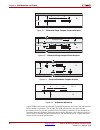
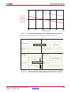
58 www.Xilinx.Com spartan-6 fpga pcb design and pin planning ug393 (v1.1) april 29, 2010 chapter 5: design of transitions for high-speed signals x-ref target - figure 5-17 figure 5-17: simulated tdr of 45 degree bends with jog-outs x-ref target - figure 5-18 figure 5-18: simulated tdr of 45 degree b...
Page 59
Spartan-6 fpga pcb design and pin planning www.Xilinx.Com 59 ug393 (v1.1) april 29, 2010 microstrip/stripline bends for wide traces, curved routing can also be helpful as shown in figure 5-20 . X-ref target - figure 5-19 figure 5-19: simulated phase response of 45 degree bends with jog-outs x-ref ta...
Page 60
60 www.Xilinx.Com spartan-6 fpga pcb design and pin planning ug393 (v1.1) april 29, 2010 chapter 5: design of transitions for high-speed signals.
Page 61: I/o Pin and Clock Planning
Spartan-6 fpga pcb design and pin planning www.Xilinx.Com 61 ug393 (v1.1) april 29, 2010 chapter 6 i/o pin and clock planning this chapter contains guidelines for pin-planning and clocking considerations when designing with spartan-6 fpgas. Choosing the correct resources enables a faster and cleaner...
Page 62: Memory Controller Block
62 www.Xilinx.Com spartan-6 fpga pcb design and pin planning ug393 (v1.1) april 29, 2010 chapter 6: i/o pin and clock planning that require v ref pins in bank 1 and also use the bpi configuration mode. Designers need to review the tradeoffs before dedicating multi-function pins. Designs using the ma...
Page 63: Pci
Spartan-6 fpga pcb design and pin planning www.Xilinx.Com 63 ug393 (v1.1) april 29, 2010 pci all supported mcb interfaces (with the exception of lpddr) require the use of the v ref pins to provide the appropriate voltage reference. Therefore, for all memory interfaces (except lpddr), the multi-funct...
Page 64: Global and I/o Clocking
64 www.Xilinx.Com spartan-6 fpga pcb design and pin planning ug393 (v1.1) april 29, 2010 chapter 6: i/o pin and clock planning gtp transceiver clocking considerations gtp transceivers use bufio2 clock buffers to reach the dcm, pll, and bufg resources for fpga logic clocking. From one to all eight bu...
Page 65
Spartan-6 fpga pcb design and pin planning www.Xilinx.Com 65 ug393 (v1.1) april 29, 2010 global and i/o clocking a gclk pin to bufg connectivity check will ensure that there are no gclk pin assignment conflicts for the same bufg global clock line. See the shared global clocking resources tables (cha...
Page 66: Serializing Interfaces
66 www.Xilinx.Com spartan-6 fpga pcb design and pin planning ug393 (v1.1) april 29, 2010 chapter 6: i/o pin and clock planning overview of bufio2 resource usage per interface type • each single-ended sdr interface consumes one bufio2 buffer. • each single-ended ddr interface consumes two bufio2 buff...
Page 67: Running Design Rule Checks
Spartan-6 fpga pcb design and pin planning www.Xilinx.Com 67 ug393 (v1.1) april 29, 2010 power management—using suspend/awake differential serdes differential i/o can be serialized up to 8:1 with each p/n differential pair. Power management—using suspend/awake when using the suspend function, the fu...
Page 68: Density Migration
68 www.Xilinx.Com spartan-6 fpga pcb design and pin planning ug393 (v1.1) april 29, 2010 chapter 6: i/o pin and clock planning of routing through the device (from inputs, to internal logic, to outputs). See wp311 : improving performance in spartan-6 fpga designs for a discussion on this topic. Densi...
Page 69: Recommended Pcb Design Rules
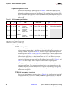
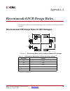
Spartan-6 fpga pcb design and pin planning www.Xilinx.Com 69 ug393 (v1.1) april 29, 2010 appendix a recommended pcb design rules this appendix outlines the recommended design rules for all the available spartan-6 fpga packages. Recommended pcb design rules for qfp packages x-ref target - figure a-1 ...
Page 70
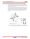
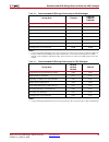
70 www.Xilinx.Com spartan-6 fpga pcb design and pin planning ug393 (v1.1) april 29, 2010 appendix a: recommended pcb design rules recommended pcb design rules for bga and csp packages xilinx provides the diameter of a land pad on the component side. This information is required prior to the start of...
Page 71
Spartan-6 fpga pcb design and pin planning www.Xilinx.Com 71 ug393 (v1.1) april 29, 2010 recommended pcb design rules for bga and csp packages table a-2: recommended pcb design rules (mm) for bga packages design rule ft(g)256 fg(g)484 fg(g)676 fg(g)900 component land pad diameter (smd) (1) 0.40 0.45...
Page 72
72 www.Xilinx.Com spartan-6 fpga pcb design and pin planning ug393 (v1.1) april 29, 2010 appendix a: recommended pcb design rules.


