- DL manuals
- Xilinx
- Transceiver
- Virtex-6 FPGA
- Manual
Xilinx Virtex-6 FPGA Manual
Summary of Virtex-6 FPGA
Page 1
Virtex-6 libraries guide for hdl designs ug623 (v 14.5) march 20, 2013.
Page 2
Notice of disclaimer the information disclosed to you hereunder (the "materials") is provided solely for the selection and use of xilinx products. To the maximum extent permitted by applicable law: (1) materials are made available "as is" and with all faults, xilinx hereby disclaims all warranties a...
Page 3: Introduction
Chapter 1 introduction this hdl guide is part of the ise® documentation collection. A separate version of this guide is available if you prefer to work with schematics. This guide contains the following: • introduction. • descriptions of each available macro. • a list of design elements supported in...
Page 4: Design Entry Methods
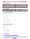
Chapter 1: introduction design entry methods for each design element in this guide, xilinx evaluates four options for using the design element, and recommends what we believe is the best solution for you. The four options are: • instantiation - this component can be instantiated directly into the de...
Page 5: About Unimacros
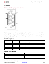
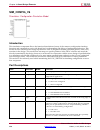
Chapter 2 about unimacros this section describes the unimacros that can be used with virtex®-6 devices. The unimacros are organized alphabetically. The following information is provided for each unimacro, where applicable: • name of element • brief description • schematic symbol • logic table (if an...
Page 6: Bram_Sdp_Macro
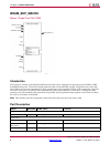
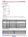
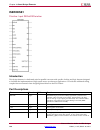
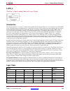
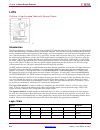
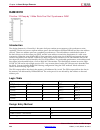
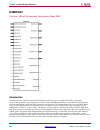
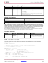
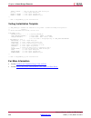
Chapter 2: about unimacros bram_sdp_macro macro: simple dual port ram introduction fpga devices contain several block ram memories that can be configured as general-purpose 36kb or 18kb ram/rom memories. These block ram memories offer fast and flexible storage of large amounts of on-chip data. Both ...
Page 7
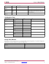
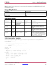
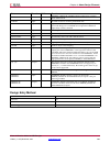
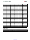
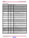
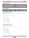
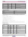
Chapter 2: about unimacros name direction width (bits) function wren, rden input 1 write/read enable ssr input 1 output registers synchronous reset. Regce input 1 output register clock enable input (valid only when do_reg=1) wrclk, rdclk input 1 write/read clock input. Configuration table data_width...
Page 8
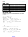
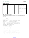
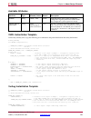
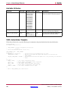
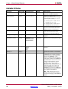
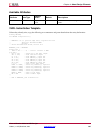
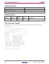
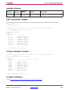
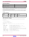
Chapter 2: about unimacros available attributes attribute data type allowed values default description bram_size string "36kb", "18kb" "18kb" configures ram as "36kb" or "18kb" memory. Do_reg integer 0, 1 0 a value of 1 enables to the output registers to the ram enabling quicker clock-to-out from th...
Page 9
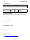
Chapter 2: about unimacros attribute data type allowed values default description sim_mode string "safe", "fast" . "safe" this is a simulation only attribute. It will direct the simulation model to run in performance-oriented mode when set to "fast." please see the synthesis and simulation design gu...
Page 10
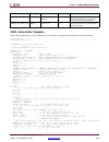
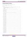
Chapter 2: about unimacros init_02 => x"0000000000000000000000000000000000000000000000000000000000000000", init_03 => x"0000000000000000000000000000000000000000000000000000000000000000", init_04 => x"0000000000000000000000000000000000000000000000000000000000000000", init_05 => x"00000000000000000000...
Page 11
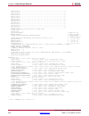
Chapter 2: about unimacros init_49 => x"0000000000000000000000000000000000000000000000000000000000000000", init_4a => x"0000000000000000000000000000000000000000000000000000000000000000", init_4b => x"0000000000000000000000000000000000000000000000000000000000000000", init_4c => x"00000000000000000000...
Page 12
Chapter 2: about unimacros initp_0e => x"0000000000000000000000000000000000000000000000000000000000000000", initp_0f => x"0000000000000000000000000000000000000000000000000000000000000000") port map ( do => do, -- output read data port, width defined by read_width parameter di => di, -- input write d...
Page 13
Chapter 2: about unimacros .Init_10(256’h0000000000000000000000000000000000000000000000000000000000000000), .Init_11(256’h0000000000000000000000000000000000000000000000000000000000000000), .Init_12(256’h0000000000000000000000000000000000000000000000000000000000000000), .Init_13(256’h0000000000000000...
Page 14
Chapter 2: about unimacros .Init_57(256’h0000000000000000000000000000000000000000000000000000000000000000), .Init_58(256’h0000000000000000000000000000000000000000000000000000000000000000), .Init_59(256’h0000000000000000000000000000000000000000000000000000000000000000), .Init_5a(256’h0000000000000000...
Page 15
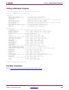
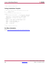
Chapter 2: about unimacros ); // end of bram_sdp_macro_inst instantiation for more information see the virtex-6 fpga user documentation (user guides and data sheets) . Virtex-6 libraries guide for hdl designs ug623 (v 14.5) march 20, 2013 www.Xilinx.Com 15.
Page 16: Bram_Single_Macro
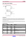
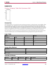
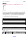
Chapter 2: about unimacros bram_single_macro macro: single port ram introduction fpga devices contain several block ram memories that can be configured as general-purpose 36kb or 18kb ram/rom memories. These single-port, block ram memories offer fast and flexible storage of large amounts of on-chip ...
Page 17
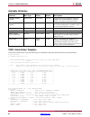
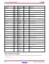
Chapter 2: about unimacros configuration table write_width read_width bram_size addr we 37 - 72 9 36 - 19 10 18 - 10 11 9 - 5 12 4 - 3 13 2 14 37 - 72 1 36kb 15 8 36 - 19 10 18-10 11 9 - 5 12 4 - 3 13 2 14 36 - 19 1 36kb 15 4 36 - 19 11 18-10 11 9 - 5 12 4 - 3 13 2 14 18 - 10 1 36kb 15 2 36-19 12 18...
Page 18
Chapter 2: about unimacros write_width read_width bram_size addr we 36 - 19 15 18 - 10 15 9 - 5 15 3 - 4 15 2 15 1 1 36kb 15 1 18-10 10 9 - 5 11 4 - 3 12 2 13 18-10 1 18kb 14 2 18-10 11 9 - 5 11 4 - 3 12 2 13 9 - 5 1 18kb 14 1 18-10 12 9 - 5 12 4 - 3 12 2 13 4 - 3 1 18kb 14 1 18-10 13 9 - 5 13 4 - 3...
Page 19
Chapter 2: about unimacros design entry method this unimacro can be instantiated only. It is a parameterizable version of the primitive. Consult the above configuration table in correctly configuring this element to meet your design needs. Instantiation yes inference no core generator™ and wizards n...
Page 20
Chapter 2: about unimacros library unisim; use unisim.Vcomponents.All; -- bram_single_macro: single port ram -- virtex-6 -- xilinx hdl libraries guide, version 14.5 -- note - this unimacro model assumes the port directions to be "downto". -- simulation of this model with "to" in the port directions ...
Page 21
Chapter 2: about unimacros init_1e => x"0000000000000000000000000000000000000000000000000000000000000000", init_1f => x"0000000000000000000000000000000000000000000000000000000000000000", init_20 => x"0000000000000000000000000000000000000000000000000000000000000000", init_21 => x"00000000000000000000...
Page 22
Chapter 2: about unimacros init_65 => x"0000000000000000000000000000000000000000000000000000000000000000", init_66 => x"0000000000000000000000000000000000000000000000000000000000000000", init_67 => x"0000000000000000000000000000000000000000000000000000000000000000", init_68 => x"00000000000000000000...
Page 24
Chapter 2: about unimacros .Init_31(256’h0000000000000000000000000000000000000000000000000000000000000000), .Init_32(256’h0000000000000000000000000000000000000000000000000000000000000000), .Init_33(256’h0000000000000000000000000000000000000000000000000000000000000000), .Init_34(256’h0000000000000000...
Page 25
Chapter 2: about unimacros .Init_78(256’h0000000000000000000000000000000000000000000000000000000000000000), .Init_79(256’h0000000000000000000000000000000000000000000000000000000000000000), .Init_7a(256’h0000000000000000000000000000000000000000000000000000000000000000), .Init_7b(256’h0000000000000000...
Page 26: Bram_Tdp_Macro
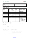
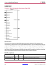
Chapter 2: about unimacros bram_tdp_macro macro: true dual port ram introduction fpga devices contain several block ram memories that can be configured as general-purpose 36kb or 18kb ram/rom memories. These block ram memories offer fast and flexible storage of large amounts of on-chip data. Both re...
Page 27
Chapter 2: about unimacros name direction width function dib input see configuration table below. Data input bus addressed by addrb. Addra, addrb input see configuration table below. Address input buses for port a, b. Wea, web input see configuration table below. Write enable for port a, b. Ena, enb...
Page 28
Chapter 2: about unimacros write_width_a/b- dia/dib read_width_a/b- doa/dob bram_size addra/b wea/b 36-19 14 18-10 14 9 - 5 14 4 - 3 14 2 14 2 1 36kb 15 1 36-19 15 18-10 15 9 - 5 15 4 - 3 15 2 15 1 1 36kb 15 1 18-10 10 9 - 5 11 4 - 3 12 2 13 18-10 1 18kb 14 2 18-10 11 9 - 5 11 4 - 3 12 2 13 9 - 5 1 ...
Page 29
Chapter 2: about unimacros design entry method this unimacro can be instantiated only. It is a parameterizable version of the primitive. Consult the configuration table above to correctly configure it to meet your design needs. Instantiation yes inference no core generator™ and wizards no macro supp...
Page 30
Chapter 2: about unimacros attribute(s) data type allowed values default description sim_mode string "safe", "fast" . "safe" this is a simulation only attribute. It will direct the simulation model to run in performance-oriented mode when set to "fast." please see the synthesis and simulation design...
Page 31
Chapter 2: about unimacros init_01 => x"0000000000000000000000000000000000000000000000000000000000000000", init_02 => x"0000000000000000000000000000000000000000000000000000000000000000", init_03 => x"0000000000000000000000000000000000000000000000000000000000000000", init_04 => x"00000000000000000000...
Page 32
Chapter 2: about unimacros init_48 => x"0000000000000000000000000000000000000000000000000000000000000000", init_49 => x"0000000000000000000000000000000000000000000000000000000000000000", init_4a => x"0000000000000000000000000000000000000000000000000000000000000000", init_4b => x"00000000000000000000...
Page 33
Chapter 2: about unimacros initp_0d => x"0000000000000000000000000000000000000000000000000000000000000000", initp_0e => x"0000000000000000000000000000000000000000000000000000000000000000", initp_0f => x"0000000000000000000000000000000000000000000000000000000000000000") port map ( doa => doa, -- outp...
Page 34
Chapter 2: about unimacros .Init_07(256’h0000000000000000000000000000000000000000000000000000000000000000), .Init_08(256’h0000000000000000000000000000000000000000000000000000000000000000), .Init_09(256’h0000000000000000000000000000000000000000000000000000000000000000), .Init_0a(256’h0000000000000000...
Page 35
Chapter 2: about unimacros .Init_4e(256’h0000000000000000000000000000000000000000000000000000000000000000), .Init_4f(256’h0000000000000000000000000000000000000000000000000000000000000000), .Init_50(256’h0000000000000000000000000000000000000000000000000000000000000000), .Init_51(256’h0000000000000000...
Page 36
Chapter 2: about unimacros .Dob(dob), // output port-b data, width defined by read_width_b parameter .Addra(addra), // input port-a address, width defined by port a depth .Addrb(addrb), // input port-b address, width defined by port b depth .Clka(clka), // 1-bit input port-a clock .Clkb(clkb), // 1-...
Page 37: Addmacc_Macro
Chapter 2: about unimacros addmacc_macro macro: adder/multiplier/accumulator introduction the addmacc _macro simplifies the instantiation of the dsp48 block when used as a pre-add, multiply accumulate function. It features parameterizable input and output widths and latency that ease the integration...
Page 38
Chapter 2: about unimacros name direction width function load_data input variable, see width_product attribute. In a dsp slice, when load is asserted, loads p with a*b+load_data. Rst input 1 synchronous reset design entry method this unimacro can be instantiated only. It is a parameterizable version...
Page 39
Chapter 2: about unimacros width_preadd => 25, -- pre-adder input bus width, 1-25 width_multiplier => 18, -- multiplier input bus width, 1-18 width_product => 48) -- macc output width, 1-48 port map ( product => product, -- macc result output, width defined by width_product generic multiplier => mul...
Page 40: Addsub_Macro
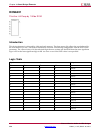
Chapter 2: about unimacros addsub_macro macro: adder/subtractor introduction the addsub_macro simplifies the instantiation of the dsp48 block when used as a simple adder/subtractor. It features parameterizable input and output widths and latency that ease the integration of the dsp48 block into hdl....
Page 41
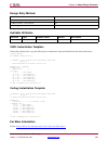
Chapter 2: about unimacros instantiation yes inference no core generator™ and wizards no macro support recommended available attributes attribute data type allowed values default description device string "virtex6", "spartan6" "virtex6" target hardware architecture. Latency integer 0, 1, 2 2 number ...
Page 42
Chapter 2: about unimacros verilog instantiation template // addsub_macro: variable width & latency - adder / subtracter implemented in a dsp48e // virtex-6 // xilinx hdl libraries guide, version 14.5 addsub_macro #( .Device("virtex6"), // target device: "virtex5", "virtex6", "spartan6" .Latency(2),...
Page 43: Counter_Load_Macro
Chapter 2: about unimacros counter_load_macro macro: loadable counter introduction the counter_load_macro simplifies the instantiation of the dsp48 block when used as dynamic loading up/down counter. It features parameterizable output width and count by values that ease the integration of the dsp48 ...
Page 44
Chapter 2: about unimacros instantiation yes inference no core generator™ and wizards no macro support recommended available attributes attribute data type allowed values default description device string "virtex6", "spartan6" "virtex6" target hardware architecture. Count_by hexa- decimal any 48 bit...
Page 45
Chapter 2: about unimacros // end of counter_load_macro_inst instantiation for more information see the virtex-6 fpga user documentation (user guides and data sheets) . Virtex-6 libraries guide for hdl designs ug623 (v 14.5) march 20, 2013 www.Xilinx.Com 45.
Page 46: Counter_Tc_Macro
Chapter 2: about unimacros counter_tc_macro macro: counter with terminal count introduction the counter_tc_macro simplifies the instantiation of the dsp48 block when used as a terminal count, up/down counter. It features parameterizable output width, terminal count values, count by and count directi...
Page 47
Chapter 2: about unimacros available attributes attribute data type allowed values default description reset_upon_tc boolean true, false false specifies whether to reset the counter upon reaching terminal count device string "virtex6", "spartan6" "virtex6" target hardware architecture. Direction str...
Page 48
Chapter 2: about unimacros // end of counter_tc_macro_inst instantiation for more information see the virtex-6 fpga user documentation (user guides and data sheets) . Virtex-6 libraries guide for hdl designs 48 www.Xilinx.Com ug623 (v 14.5) march 20, 2013.
Page 49: Eq_Compare_Macro
Chapter 2: about unimacros eq_compare_macro macro: equality comparator introduction the eq_compare_macro simplifies the instantiation of the dsp48 block when used as an equality comparator. It features parameterizable input and output widths, latencies, mask, and input sources that ease the integrat...
Page 50
Chapter 2: about unimacros instantiation yes inference no core generator™ and wizards no macro support recommended available attributes attribute data type allowed values default description device string "virtex5", "virtex6", "spartan6" "virtex6" target hardware architecture. Sel_pattern integer 1 ...
Page 51
Chapter 2: about unimacros clk => clk, -- 1-bit positive edge clock input data_in => data_in, -- input data bus, width determined by width generic dynamic_pattern, => dynamic_pattern, -- input dynamic match/mask bus, width determined by width generic rst => rst -- 1-bit input active high reset ); --...
Page 52: Macc_Macro
Chapter 2: about unimacros macc_macro macro: multiplier/accumulator introduction the macc_macro simplifies the instantiation of the dsp48 block when used in simple signed multiplier/accumulator mode. It features parameterizable input and output widths and latencies that ease the integration of the d...
Page 53
Chapter 2: about unimacros name direction width function rst input 1 synchronous reset. Addsub input 1 high sets accumulator in addition mode; low sets accumulator in subtraction mode. Design entry method this unimacro can be instantiated only. It is a parameterizable version of the primitive. Insta...
Page 54
Chapter 2: about unimacros carryin => carryin, -- 1-bit carry-in input to accumulator ce => ce, -- 1-bit active high input clock enable clk => clk, -- 1-bit positive edge clock input load => load, -- 1-bit active high input load accumulator enable load_data => load_data, -- load accumulator input da...
Page 55: Mult_Macro
Chapter 2: about unimacros mult_macro macro: multiplier introduction the mult_macro simplifies the instantiation of the dsp48 block when used as a simple signed multiplier. It features parameterizable input and output widths and latencies that ease the integration of the dsp48 block into hdl. Port d...
Page 56
Chapter 2: about unimacros available attributes attribute data type allowed values default description width_a integer 1 to 25 25 controls the width of a input. Width_b integer 1 to 18 18 controls the width of b input. Latency integer 0, 1, 2, 3, 4 3 number of pipeline registers • 1 - mreg == 1 • 2 ...
Page 57
Chapter 2: about unimacros .Rst(rst) // 1-bit input active high reset ); // end of mult_macro_inst instantiation for more information see the virtex-6 fpga user documentation (user guides and data sheets) . Virtex-6 libraries guide for hdl designs ug623 (v 14.5) march 20, 2013 www.Xilinx.Com 57.
Page 58: Fifo_Dualclock_Macro
Chapter 2: about unimacros fifo_dualclock_macro macro: dual clock first-in, first-out (fifo) ram buffer introduction fpga devices contain several block ram memories that can be configured as general-purpose 36kb or 18kb ram/rom memories. Dedicated logic in the block ram enables you to easily impleme...
Page 59
Chapter 2: about unimacros name direction width function wrcount output see configuration table below. Fifo data write pointer. Wrerr output 1 when the fifo is full, any additional write operation generates an error flag. Input ports di input see configuration table below. Data input bus addressed b...
Page 60
Chapter 2: about unimacros available attributes attribute data type allowed values default description almost_empty_ offset hexadecimal 13-bit value all zeros setting determines the difference between empty and almostempty conditions. Must be set using hexadecimal notation. Almost_full_ offset hexad...
Page 61
Chapter 2: about unimacros rdcount => rdcount, -- output read count, width determined by fifo depth rderr => rderr, -- 1-bit output read error wrcount => wrcount, -- output write count, width determined by fifo depth wrerr => wrerr, -- 1-bit output write error di => di, -- input data, width defined ...
Page 62: Fifo_Sync_Macro
Chapter 2: about unimacros fifo_sync_macro macro: synchronous first-in, first-out (fifo) ram buffer introduction fpga devices contain several block ram memories that can be configured as general-purpose 36kb or 18kb ram/rom memories. Dedicated logic in the block ram enables you to easily implement f...
Page 63
Chapter 2: about unimacros name direction width function input ports clk input 1 clock for read/write domain operation. Di input see configuration table. Data input bus addressed by addr. Rden input 1 read enable rst input 1 asynchronous reset. Wren input 1 write enable configuration table this unim...
Page 64
Chapter 2: about unimacros available attributes attribute data type allowed values default description almost_empty_ offset hexadecimal any 13-bit value all zeros setting determines the difference between empty and almostempty conditions. Must be set using hexadecimal notation. Almost_full_ offset h...
Page 65
Chapter 2: about unimacros do => do, -- output data, width defined by data_width parameter empty => empty, -- 1-bit output empty full => full, -- 1-bit output full rdcount => rdcount, -- output read count, width determined by fifo depth rderr => rderr, -- 1-bit output read error wrcount => wrcount, ...
Page 66
Virtex-6 libraries guide for hdl designs 66 www.Xilinx.Com ug623 (v 14.5) march 20, 2013.
Page 67: Functional Categories
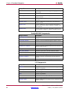
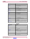
Chapter 3 functional categories this section categorizes, by function, the circuit design elements described in detail later in this guide. The elements ( primitives and macros ) are listed in alphanumeric order under each functional category. Advanced config/bscan components registers/latches arith...
Page 68
Chapter 3: functional categories design element description bufhce primitive: clock buffer for a single clocking region with clock enable bufio primitive: local clock buffer for i/o bufiodqs primitive: differential clock input for transceiver reference clocks bufr primitive: regional clock buffer fo...
Page 69
Chapter 3: functional categories design element description ibufg primitive: dedicated input clock buffer ibufgds primitive: differential signaling dedicated input clock buffer and optional delay ibufgds_diff_out primitive: differential signaling input buffer with differential output idelayctrl prim...
Page 70
Chapter 3: functional categories design element description ram32x2s primitive: 32-deep by 2-wide static synchronous ram ram64m primitive: 64-deep by 4-bit wide multi port random access memory (select ram) ram64x1d primitive: 64-deep by 1-wide dual port static synchronous ram ram64x1s primitive: 64-...
Page 71
Chapter 3: functional categories slice/clb primitives design element description carry4 primitive: fast carry logic with look ahead cfglut5 primitive: 5-input dynamically reconfigurable look-up table (lut) lut1 macro: 1-bit look-up table with general output lut1_d macro: 1-bit look-up table with dua...
Page 72
Virtex-6 libraries guide for hdl designs 72 www.Xilinx.Com ug623 (v 14.5) march 20, 2013.
Page 73: About Design Elements
Chapter 4 about design elements this section describes the design elements that can be used with virtex®-6 devices. The design elements are organized alphabetically. The following information is provided for each design element, where applicable: • name of element • brief description • schematic sym...
Page 74: Bscan_Virtex6
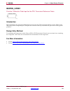
Chapter 4: about design elements bscan_virtex6 primitive: virtex®-6 jtag boundary-scan logic access circuit introduction this design element allows access to and from internal logic by the jtag boundary scan logic controller. This allows for communication between the internal running design and the ...
Page 75
Chapter 4: about design elements design entry method instantiation recommended inference no core generator™ and wizards no macro support no available attributes attribute data type allowed values default description jtag_chain integer 1, 2, 3, 4 1 sets the jtag user instruction number that this inst...
Page 76
Chapter 4: about design elements .Shift(shift), // 1-bit output: shift output from tap controller .Tck(tck), // 1-bit output: scan clock output. Fabric connection to tap clock pin. .Tdi(tdi), // 1-bit output: tdi output from tap controller .Tms(tms), // 1-bit output: test mode select input. Fabric c...
Page 77: Bufg
Chapter 4: about design elements bufg primitive: global clock buffer introduction this design element is a high-fanout buffer that connects signals to the global routing resources for low skew distribution of the signal. Bufgs are typically used on clock nets as well other high fanout nets like sets...
Page 78
Chapter 4: about design elements verilog instantiation template // bufg: global clock buffer // virtex-6 // xilinx hdl libraries guide, version 14.5 bufg bufg_inst ( .O(o), // 1-bit output: clock buffer output .I(i) // 1-bit input: clock buffer input ); // end of bufg_inst instantiation for more inf...
Page 79: Bufgce
Chapter 4: about design elements bufgce primitive: global clock buffer with clock enable introduction this design element is a global clock buffer with a single gated input. Its o output is "0" when clock enable (ce) is low (inactive). When clock enable (ce) is high, the i input is transferred to th...
Page 80
Chapter 4: about design elements verilog instantiation template // bufgce: global clock buffer with clock enable // virtex-6 // xilinx hdl libraries guide, version 14.5 bufgce bufgce_inst ( .O(o), // 1-bit output: clock buffer output .Ce(ce), // 1-bit input: clock enable input for i0 input .I(i) // ...
Page 81: Bufgce_1
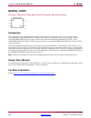
Chapter 4: about design elements bufgce_1 primitive: global clock buffer with clock enable and output state 1 introduction this design element is a multiplexed global clock buffer with a single gated input. Its o output is high (1) when clock enable (ce) is low (inactive). When clock enable (ce) is ...
Page 82
Chapter 4: about design elements -- end of bufgce_1_inst instantiation verilog instantiation template // bufgce_1: global clock buffer with clock enable and output state 1 // virtex-6 // xilinx hdl libraries guide, version 14.5 bufgce_1 bufgce_1_inst ( .O(o), // 1-bit output: clock buffer output .Ce...
Page 83: Bufgctrl
Chapter 4: about design elements bufgctrl primitive: global clock mux buffer introduction bufgctrl primitive is global clock buffer that is designed as a synchronous/asynchronous "glitch free" 2:1 multiplexer with two clock inputs. Unlike global clock buffers that are found in previous generation of...
Page 84
Chapter 4: about design elements available attributes attribute data type allowed values default description init_out integer 0, 1 0 initializes the bufgctrl output to the specified value after configuration. Preselect_i0 boolean false, true false if true, bufgctrl output uses i0 input after configu...
Page 85
Chapter 4: about design elements ); // end of bufgctrl_inst instantiation for more information see the virtex-6 fpga user documentation (user guides and data sheets) . Virtex-6 libraries guide for hdl designs ug623 (v 14.5) march 20, 2013 www.Xilinx.Com 85.
Page 86: Bufgmux
Chapter 4: about design elements bufgmux primitive: global clock mux buffer introduction bufgmux is a multiplexed global clock buffer that can select between two input clocks: i0 and i1. When the select input (s) is low, the signal on i0 is selected for output (o). When the select input (s) is high,...
Page 87
Chapter 4: about design elements vhdl instantiation template unless they already exist, copy the following two statements and paste them before the entity declaration. Library unisim; use unisim.Vcomponents.All; -- bufgmux: global clock mux buffer -- virtex-6 -- xilinx hdl libraries guide, version 1...
Page 88: Bufgmux_1
Chapter 4: about design elements bufgmux_1 primitive: global clock mux buffer with output state 1 introduction this design element is a multiplexed global clock buffer that can select between two input clocks: i0 and i1. When the select input (s) is low, the signal on i0 is selected for output (0). ...
Page 89
Chapter 4: about design elements vhdl instantiation template unless they already exist, copy the following two statements and paste them before the entity declaration. Library unisim; use unisim.Vcomponents.All; -- bufgmux_1: global clock mux buffer with output state 1 -- virtex-6 -- xilinx hdl libr...
Page 90: Bufgmux_Ctrl
Chapter 4: about design elements bufgmux_ctrl primitive: 2-to-1 global clock mux buffer introduction this design element is a global clock buffer with two clock inputs, one clock output, and a select line used to cleanly select between one of two clocks driving the global clocking resource. This com...
Page 91
Chapter 4: about design elements vhdl instantiation template unless they already exist, copy the following two statements and paste them before the entity declaration. Library unisim; use unisim.Vcomponents.All; -- bufgmux_ctrl: 2-to-1 global clock mux buffer -- virtex-6 -- xilinx hdl libraries guid...
Page 92: Bufh
Chapter 4: about design elements bufh primitive: clock buffer for a single clocking region introduction the bufh primitive is provided to allow instantiation capability to access the hclk clock buffer resources. The use of this component requires manual placement and special consideration and thus i...
Page 93
Chapter 4: about design elements verilog instantiation template // bufh: hrow clock buffer for a single clocking region // virtex-6 // xilinx hdl libraries guide, version 14.5 bufh bufh_inst ( .O(o), // 1-bit output: clock output .I(i) // 1-bit input: clock input ); // end of bufh_inst instantiation...
Page 94: Bufhce
Chapter 4: about design elements bufhce primitive: clock buffer for a single clocking region with clock enable introduction this element is provided to allow instantiation access to hclk clock buffer resources. In addition, it allows for power reduction capabilities through disabling of the clock vi...
Page 95
Chapter 4: about design elements ); -- end of bufhce_inst instantiation verilog instantiation template // bufhce: hrow clock buffer for a single clocking region with clock enable // virtex-6 // xilinx hdl libraries guide, version 14.5 bufhce #( .Init_out(0) // initial output value ) bufhce_inst ( .O...
Page 96: Bufio
Chapter 4: about design elements bufio primitive: local clock buffer for i/o introduction this design element is a clock buffer. It is simply a clock-in, clock-out buffer. It drives a dedicated clock net within the i/o column, independent of the global clock resources. Thus, these elements are ideal...
Page 97
Chapter 4: about design elements verilog instantiation template // bufio: local clock buffer // virtex-6 // xilinx hdl libraries guide, version 14.5 bufio bufio_inst ( .O(o), // clock buffer output .I(i) // clock buffer input ); // end of bufio_inst instantiation for more information see the virtex-...
Page 98: Bufiodqs
Chapter 4: about design elements bufiodqs primitive: differential clock input for transceiver reference clocks introduction this element is the same clock buffer as bufio with added dedicated circuitry (ideally used for memory applications) to optionally remove the extra bufio delay and also squelch...
Page 99: Bufr
Chapter 4: about design elements bufr primitive: regional clock buffer for i/o and logic resources introduction the regional clock buffer (bufr) is another available clock buffer. Bufrs drive clock signals to a dedicated clock net within a clock region, independent from the global clock tree. Each b...
Page 100
Chapter 4: about design elements available attributes attribute data type allowed_values default description bufr_divide string "bypass", "1", "2", "3", "4", "5", "6", "7", "8" "bypass" defines whether the output clock is a divided version of input clock. Sim_device string "virtex4", virtex5", "virt...
Page 101: Capture_Virtex6
Chapter 4: about design elements capture_virtex6 primitive: virtex®-6 readback register capture control introduction this element provides user control and synchronization over when and how the capture register (flip-flop and latch) information task is requested. The readback function is provided th...
Page 102
Chapter 4: about design elements vhdl instantiation template unless they already exist, copy the following two statements and paste them before the entity declaration. Library unisim; use unisim.Vcomponents.All; -- capture_virtex6: register capture -- virtex-6 -- xilinx hdl libraries guide, version ...
Page 103: Carry4
Chapter 4: about design elements carry4 primitive: fast carry logic with look ahead introduction this circuit design represents the fast carry logic for a slice. The carry chain consists of a series of four muxes and four xors that connect to the other logic (luts) in the slice via dedicated routes ...
Page 104
Chapter 4: about design elements vhdl instantiation template unless they already exist, copy the following two statements and paste them before the entity declaration. Library unisim; use unisim.Vcomponents.All; -- carry4: fast carry logic component -- virtex-6 -- xilinx hdl libraries guide, version...
Page 105: Cfglut5
Chapter 4: about design elements cfglut5 primitive: 5-input dynamically reconfigurable look-up table (lut) introduction this element is a runtime, dynamically reconfigurable, 5-input look-up table (lut) that enables the changing of the logical function of the lut during circuit operation. Using the ...
Page 106
Chapter 4: about design elements design entry method instantiation recommended inference no core generator™ and wizards no macro support no • connect the clk input to the clock source used to supply the reconfiguration data. • connect the cdi input to the source of the reconfiguration data. • connec...
Page 107
Chapter 4: about design elements vhdl instantiation template unless they already exist, copy the following two statements and paste them before the entity declaration. Library unisim; use unisim.Vcomponents.All; -- cfglut5: reconfigurable 5-input lut -- virtex-6 -- xilinx hdl libraries guide, versio...
Page 108: Dcireset
Chapter 4: about design elements dcireset primitive: dci state machine reset (after configuration has been completed) introduction this design element is used to reset the dci state machine after configuration has been completed. Port descriptions port direction width function locked output 1 dcires...
Page 109
Chapter 4: about design elements for more information see the virtex-6 fpga user documentation (user guides and data sheets) . Virtex-6 libraries guide for hdl designs ug623 (v 14.5) march 20, 2013 www.Xilinx.Com 109.
Page 110: Dna_Port
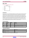
Chapter 4: about design elements dna_port primitive: device dna data access port introduction this element allows access to a dedicated shift register that can be loaded with the device dna data bits (unique id) for a given device. In addition to shifting out the dna data bits, this component allows...
Page 111
Chapter 4: about design elements available attributes attribute data type allowed values default description sim_dna_value hexa- decimal 57’h00000000 0000000 to 57’h1ffffffffffffff 57’h00000000 0000000 specifies the pre-programmed factory id value. Vhdl instantiation template unless they already exi...
Page 112: Dsp48E1
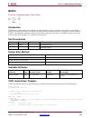
Chapter 4: about design elements dsp48e1 primitive: 25x18 two’s complement multiplier with integrated 48-bit, 3-input adder/subtracter/accumulator or 2-input logic unit introduction this design element is a versatile, scalable, hard ip block within virtex®-6 that allows for the creation of compact, ...
Page 113
Chapter 4: about design elements port descriptions port direction width function a[29:0] input 30 25-bit data input to multiplier, pre-adder, or 30-bit msb data input to adder/logic unit. Tie port to all ones if not used. Acin[29:0] input 30 cascade input for port a. If used, connect to acout of ups...
Page 114
Chapter 4: about design elements port direction width function ceb1 input 1 active high, clock enable for the first b (input) register. This port is only used if breg = 2 or inmode0 = 1. Tie to logic one if not used and breg=2. When two registers are used, this is the first sequentially. When dynami...
Page 115
Chapter 4: about design elements port direction width function pcin[47:0] input 48 cascade input for port p. If used, connect to pcout of upstream cascaded dsp slice. If not used, tie port to all zeros. Pcout[47:0] output 48 cascade output for port p. If used, connect to pcin of downstream cascaded ...
Page 116
Chapter 4: about design elements attribute data type allowed values default description areg integer 1, 0, 2 1 selects number of pipeline stages for the a input. Autoreset_ patdet string "no_reset", "reset_match", "reset_not_ match" "no_reset" automatically reset dsp slice p register (accumulated va...
Page 117
Chapter 4: about design elements attribute data type allowed values default description use_mult string "multiply", "dynamic", "none" "multiply" selects usage of the multiplier. Set to none to save power when using only the adder/logic unit. The dynamic setting indicates that the user is switching b...
Page 118
Chapter 4: about design elements -- cascade: 30-bit (each) output: cascade ports acout => acout, -- 30-bit output: a port cascade output bcout => bcout, -- 18-bit output: b port cascade output carrycascout => carrycascout, -- 1-bit output: cascade carry output multsignout => multsignout, -- 1-bit ou...
Page 119
Chapter 4: about design elements .Use_mult("multiply"), // select multiplier usage ("multiply", "dynamic", or "none") // pattern detector attributes: pattern detection configuration .Autoreset_patdet("no_reset"), // "no_reset", "reset_match", "reset_not_match" .Mask(48’h3fffffffffff), // 48-bit mask...
Page 120
Chapter 4: about design elements .Rsta(rsta), // 1-bit input: reset input for areg .Rstallcarryin(rstallcarryin), // 1-bit input: reset input for carryinreg .Rstalumode(rstalumode), // 1-bit input: reset input for alumodereg .Rstb(rstb), // 1-bit input: reset input for breg .Rstc(rstc), // 1-bit inp...
Page 121: Efuse_Usr
Chapter 4: about design elements efuse_usr primitive: 32-bit non-volatile design id introduction provides internal access via jtag to the 32 non-volatile fuses that can store bits specific to the design (e.G., a unique id associated with each design). Port descriptions port direction width function ...
Page 122
Chapter 4: about design elements verilog instantiation template // efuse_usr: 32-bit non-volatile design id // virtex-6 // xilinx hdl libraries guide, version 14.5 efuse_usr #( .Sim_efuse_value(32’h00000000) // value of the 32-bit non-volatile design id used in simulation ) efuse_usr_inst ( .Efuseus...
Page 123: Fdce
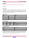
Chapter 4: about design elements fdce primitive: d flip-flop with clock enable and asynchronous clear introduction this design element is a single d-type flip-flop with clock enable and asynchronous clear. When clock enable (ce) is high and asynchronous clear (clr) is low, the data on the data input...
Page 124
Chapter 4: about design elements vhdl instantiation template unless they already exist, copy the following two statements and paste them before the entity declaration. Library unisim; use unisim.Vcomponents.All; -- fdce: single data rate d flip-flop with asynchronous clear and -- clock enable (posed...
Page 125: Fdpe
Chapter 4: about design elements fdpe primitive: d flip-flop with clock enable and asynchronous preset introduction this design element is a single d-type flip-flop with data (d), clock enable (ce), and asynchronous preset (pre) inputs and data output (q). The asynchronous pre, when high, overrides ...
Page 126
Chapter 4: about design elements vhdl instantiation template unless they already exist, copy the following two statements and paste them before the entity declaration. Library unisim; use unisim.Vcomponents.All; -- fdpe: single data rate d flip-flop with asynchronous preset and -- clock enable (pose...
Page 127: Fdre
Chapter 4: about design elements fdre primitive: d flip-flop with clock enable and synchronous reset introduction this design element is a single d-type flip-flop with data (d), clock enable (ce), and synchronous reset (r) inputs and data output (q). The synchronous reset (r) input, when high, overr...
Page 128
Chapter 4: about design elements vhdl instantiation template unless they already exist, copy the following two statements and paste them before the entity declaration. Library unisim; use unisim.Vcomponents.All; -- fdre: single data rate d flip-flop with synchronous reset and -- clock enable (posedg...
Page 129: Fdse
Chapter 4: about design elements fdse primitive: d flip-flop with clock enable and synchronous set introduction fdse is a single d-type flip-flop with data (d), clock enable (ce), and synchronous set (s) inputs and data output (q). The synchronous set (s) input, when high, overrides the clock enable...
Page 130
Chapter 4: about design elements vhdl instantiation template unless they already exist, copy the following two statements and paste them before the entity declaration. Library unisim; use unisim.Vcomponents.All; -- fdse: single data rate d flip-flop with synchronous set and -- clock enable (posedge ...
Page 131: Fifo18E1
Chapter 4: about design elements fifo18e1 primitive: 18 k-bit fifo (first in, first out) block ram memory introduction virtex®-6 devices contain several block ram memories, each of which can be separately configured as a fifo, an automatic error-correction ram, or as a general-purpose 36 kb or 18 kb...
Page 132
Chapter 4: about design elements port direction width function dop[3:0] output 4 fifo parity data output bus. Empty output 1 active high logic to indicate that the fifo is currently empty. Full output 1 active high logic indicates that the fifo is full. Rden input 1 active high fifo read enable. Reg...
Page 133
Chapter 4: about design elements attribute data type allowed values default description first_word_fall_ through boolean false, true false if true, the first write to the fifo appears on do without a first rden assertion. Init hexa- decimal any 36 bit value all zeros specifies the initial value on t...
Page 134
Chapter 4: about design elements verilog instantiation template // fifo18e1: 18kb fifo (first in, first out) block ram memory // virtex-6 // xilinx hdl libraries guide, version 14.5 fifo18e1 #( .Almost_empty_offset(13’h0080), // sets the almost empty threshold .Almost_full_offset(13’h0080), // sets ...
Page 135: Fifo36E1
Chapter 4: about design elements fifo36e1 primitive: 36 kb fifo (first in, first out) block ram memory introduction virtex®-6 devices contain several block ram memories that can be configured as fifos, automatic error-correction ram, or general-purpose 36 kb or 18 kb ram/rom memories. These block ra...
Page 136
Chapter 4: about design elements port direction width function di[63:0] input 64 fifo data input bus. Dip[7:0] input 8 fifo parity data input bus. Do[63:0] output 64 fifo data output bus. Dop[7:0] output 8 fifo parity data output bus. Eccparity[7:0] output 8 8-bit data generated by the ecc encoder u...
Page 137
Chapter 4: about design elements available attributes attribute data type allowed values default description almost_empty_ offset hexa- decimal 13’h0000 to 13’h8191 13’h0080 specifies the amount of data contents in the ram to trigger the almost_empty flag. Almost_full_ offset hexa- decimal 13’h0000 ...
Page 138
Chapter 4: about design elements ) port map ( -- ecc signals: 1-bit (each) output: error correction circuitry ports dbiterr => dbiterr, -- 1-bit output: double bit error status output eccparity => eccparity, -- 8-bit output: generated error correction parity sbiterr => sbiterr, -- 1-bit output: sing...
Page 139
Chapter 4: about design elements verilog instantiation template // fifo36e1: 36kb fifo (first in, first out) block ram memory // virtex-6 // xilinx hdl libraries guide, version 14.5 fifo36e1 #( .Almost_empty_offset(13’h0080), // sets the almost empty threshold .Almost_full_offset(13’h0080), // sets ...
Page 140: Frame_Ecc_Virtex6
Chapter 4: about design elements frame_ecc_virtex6 primitive: virtex®-6 configuration frame error detection and correction circuitry introduction this design element enables the dedicated, built-in ecc (error detection and correction circuitry) for the configuration memory of the fpga. This element ...
Page 141
Chapter 4: about design elements available attributes attribute data type allowed_values default description farsrc string "efar", "far" "efar" efar determines if the output of far[23:0] configuration register points to the far or efar. Sets configuration option register bit ctl0[7]. Frame_rbt_in_ f...
Page 142
Chapter 4: about design elements .Eccerror(eccerror), // 1-bit output: output indicating an ecc error .Eccerrorsingle(eccerrorsingle), // 1-bit output: output indicating single-bit frame ecc error detected. .Far(far), // 24-bit output: frame address register value output .Synbit(synbit), // 5-bit ou...
Page 143: Gthe1_Quad
Chapter 4: about design elements gthe1_quad primitive: gigabit transceiver virtex-6 libraries guide for hdl designs ug623 (v 14.5) march 20, 2013 www.Xilinx.Com 143.
Page 144
Chapter 4: about design elements introduction this design element represents the virtex®-6 fpga gth transceiver. Gth is the highest performance, 10g-optimized configurable transceiver in the virtex-6 fpga as part of the hxt family. Refer to virtex-6 fpga gth transceivers user guide for detailed info...
Page 145: Gtxe1
Chapter 4: about design elements gtxe1 primitive: gigabit transceiver introduction this design element represents the virtex®-6 fpga rocketio™ gtx transceiver, a power-efficient and highly configurable transceiver. Refer to virtex-6 fpga rocketio gtx transceiver user guide for detailed information r...
Page 146
Chapter 4: about design elements design entry method to instantiate this component, use the virtex-6 fpga rocketio gtx transceiver wizard or an associated core containing the component. Xilinx does not recommend direct instantiation of this component. For more information • see the virtex-6 fpga roc...
Page 147: Ibuf
Chapter 4: about design elements ibuf primitive: input buffer introduction this design element is automatically inserted (inferred) by the synthesis tool to any signal directly connected to a top-level input or in-out port of the design. You should generally let the synthesis tool infer this buffer....
Page 148
Chapter 4: about design elements vhdl instantiation template unless they already exist, copy the following two statements and paste them before the entity declaration. Library unisim; use unisim.Vcomponents.All; -- ibuf: single-ended input buffer -- virtex-6 -- xilinx hdl libraries guide, version 14...
Page 149: Ibufds
Chapter 4: about design elements ibufds primitive: differential signaling input buffer introduction this design element is an input buffer that supports low-voltage, differential signaling. In ibufds, a design level interface signal is represented as two distinct ports (i and ib), one deemed the "ma...
Page 150
Chapter 4: about design elements available attributes attribute data type allowed values default description diff_term boolean true or false false enables the built-in differential termination resistor. Iostandard string see data sheet. "default" assigns an i/o standard to the element. Vhdl instanti...
Page 151: Ibufds_Diff_Out
Chapter 4: about design elements ibufds_diff_out primitive: signaling input buffer with differential output introduction this design element is an input buffer that supports differential signaling. In ibufds_diff_out, a design level interface signal is represented as two distinct ports (i and ib), o...
Page 152
Chapter 4: about design elements available attributes attribute data type allowed values default description diff_term boolean true, false false specifies the use of the internal differential termination resistance. Iostandard string see data sheet. "default" assigns an i/o standard to the element. ...
Page 153: Ibufds_Gthe1
Chapter 4: about design elements ibufds_gthe1 primitive: differential clock input for the gth transceiver reference clocks introduction this component is the dedicated differential clock input for the gth transceiver reference clocks. There is one ibufgds_gthe1 component per gth quad and it connects...
Page 154: Ibufds_Gtxe1
Chapter 4: about design elements ibufds_gtxe1 primitive: differential clock input for the transceiver reference clocks introduction this component is the differential clock input for the transceiver reference clocks. It can also drive other clock resources such as bufg/mmcm as well as the reference ...
Page 155: Ibufg
Chapter 4: about design elements ibufg primitive: dedicated input clock buffer introduction the ibufg is a dedicated input to the device which should be used to connect incoming clocks to the fpga’s global clock routing resources. The ibufg provides dedicated connections from a top level port to the...
Page 156
Chapter 4: about design elements -- end of ibufg_inst instantiation verilog instantiation template // ibufg: single-ended global clock input buffer // virtex-6 // xilinx hdl libraries guide, version 14.5 ibufg #( .Ibuf_low_pwr("true"), // low power (true) vs. Performance (false) setting for referenc...
Page 157: Ibufgds
Chapter 4: about design elements ibufgds primitive: differential signaling dedicated input clock buffer and optional delay introduction this design element is a dedicated differential signaling input buffer for connection to the clock buffer (bufg) or mmcm. In ibufgds, a design-level interface signa...
Page 158
Chapter 4: about design elements available attributes attribute data type allowed values default description iostandard string see data sheet "default" assigns an i/o standard to the element. Vhdl instantiation template unless they already exist, copy the following two statements and paste them befo...
Page 159: Ibufgds_Diff_Out
Chapter 4: about design elements ibufgds_diff_out primitive: differential signaling input buffer with differential output introduction this design element is an input buffer that supports differential signaling. In ibufgds_diff_out, a design level interface signal is represented as two distinct port...
Page 160
Chapter 4: about design elements available attributes attribute data type allowed values default description iostandard string see data sheet "default" assigns an i/o standard to the element. Diff_term boolean true, false false specifies the use of the internal differential termination resistance. I...
Page 161: Icap_Virtex6
Chapter 4: about design elements icap_virtex6 primitive: internal configuration access port introduction this design element gives you access to the configuration functions of the fpga from the fpga fabric. Using this component, commands and data can be written to and read from the configuration log...
Page 162
Chapter 4: about design elements available attributes attribute data type allowed values default description device_id hexadecimal 32’h04244093, 32’h042ca093, 32’h042cc093, 32’h042c4093, 32’h042d0093, 32’h0423a093, 32’h0424a093, 32’h0424c093, 32’h04240093, 32’h04248093, 32’h04250093, 32’h04252093, 3...
Page 163
Chapter 4: about design elements verilog instantiation template // icap_virtex6: internal configuration access port // virtex-6 // xilinx hdl libraries guide, version 14.5 icap_virtex6 #( .Device_id(0’h4244093), // specifies the pre-programmed device id value .Icap_width("x8"), // specifies the inpu...
Page 164: Iddr
Chapter 4: about design elements iddr primitive: input dual data-rate register introduction this design element is a dedicated input register designed to receive external dual data rate (ddr) signals into xilinx® fpgas.The iddr is available with modes that present the data to the fpga fabric at the ...
Page 165
Chapter 4: about design elements note you cannot have an active set and an active reset in this component. One or both of the signals r and s must be tied to ground. Design entry method instantiation recommended inference no core generator™ and wizards no macro support no available attributes attrib...
Page 166
Chapter 4: about design elements -- end of iddr_inst instantiation verilog instantiation template // iddr: input double data rate input register with set, reset // and clock enable. // virtex-6 // xilinx hdl libraries guide, version 14.5 iddr #( .Ddr_clk_edge("opposite_edge"), // "opposite_edge", "s...
Page 167: Iddr_2Clk
Chapter 4: about design elements iddr_2clk primitive: input dual data-rate register with dual clock inputs introduction this design element is a dedicated input register designed to receive external dual data rate (ddr) signals into xilinx® fpgas. In general, you should only use the iddr_2clk for ap...
Page 168
Chapter 4: about design elements port direction width function s input 1 active high reset forcing q1 and q2 to a logic one. Can be synchronous or asynchronous based on the srtype attribute. Design entry method instantiation recommended inference no core generator™ and wizards no macro support no • ...
Page 169
Chapter 4: about design elements vhdl instantiation template unless they already exist, copy the following two statements and paste them before the entity declaration. Library unisim; use unisim.Vcomponents.All; -- iddr_2clk: dual-clock, input double data rate input register with -- set, reset and c...
Page 170: Idelayctrl
Chapter 4: about design elements idelayctrl primitive: idelay tap delay value control introduction this design element must be instantiated when using the iodelaye1. This occurs when the idelay or iserdes primitive is instantiated with the iobdelay_type attribute set to fixed or variable. The idelay...
Page 171
Chapter 4: about design elements vhdl instantiation template unless they already exist, copy the following two statements and paste them before the entity declaration. Library unisim; use unisim.Vcomponents.All; -- idelayctrl : input delay element control -- virtex-6 -- xilinx hdl libraries guide, v...
Page 172: Iobuf
Chapter 4: about design elements iobuf primitive: bi-directional buffer introduction the design element is a bidirectional single-ended i/o buffer used to connect internal logic to an external bidirectional pin. Logic table inputs bidirectional outputs t i io o 1 x z io 0 1 1 1 0 0 0 0 port descript...
Page 173
Chapter 4: about design elements available attributes attribute data type allowed values default description drive integer 2, 4, 6, 8, 12, 16, 24 12 selects output drive strength (ma) for the selectio™ buffers that use the lvttl, lvcmos12, lvcmos15, lvcmos18, lvcmos25, or lvcmos33 interface i/o stan...
Page 174: Iobufds
Chapter 4: about design elements iobufds primitive: 3-state differential signaling i/o buffer with active low output enable introduction the design element is a bidirectional buffer that supports low-voltage, differential signaling. For the iobufds, a design level interface signal is represented as ...
Page 175
Chapter 4: about design elements available attributes attribute data type allowed values default description iostandard string see data sheet "default" assigns an i/o standard to the element. Vhdl instantiation template unless they already exist, copy the following two statements and paste them befo...
Page 176: Iodelaye1
Chapter 4: about design elements iodelaye1 primitive: input and output fixed or variable delay element introduction every i/o block contains a programmable absolute delay element called iodelaye1. The iodelaye1 can be connected to an input register/iserdese1 or output register/oserdese1 block or bot...
Page 177
Chapter 4: about design elements port direction width function mode, the t port dynamically switches between the idatain and odatain paths providing an alternating input/output delay based on the direction indicated by the 3-state signal t from the ologic block. Idatain input 1 the idatain input is ...
Page 178
Chapter 4: about design elements attribute data type allowed values default description consumption is quantified in the xilinx power estimator (xpe) tool. Idelay_type string" "default", "fixed", "variable", var_loadable" "default" sets the type of tap delay line. Default delay guarantees zero hold ...
Page 179
Chapter 4: about design elements clkin => clkin, -- 1-bit input - clock access into the iodelay cntvaluein => cntvaluein, -- 5-bit input - counter value for loadable counter application datain => datain, -- 1-bit input - internal delay data idatain => idatain, -- 1-bit input - delay data input inc =...
Page 180: Iserdese1
Chapter 4: about design elements iserdese1 primitive: input serial/deserializer introduction this design element is a dedicated serial-to-parallel converter with specific clocking and logic features designed to facilitate the implementation of high-speed source-synchronous applications. It avoids th...
Page 181
Chapter 4: about design elements port direction width function memory_qdr mode clkb should be connected to a unique, phase shifted clock clkdiv input 1 divided clock to be used for parallelized data. D input 1 input data to be connected directly to the top-level input or i/o port of the design or to...
Page 182
Chapter 4: about design elements available attributes attribute data type allowed values default description data_rate string "ddr", "sdr" "ddr" enables incoming data stream to be processed as sdr or ddr data. Data_width integer 4, 2, 3, 5, 6, 7, 8, 10 4 defines the width of the serial-to-parallel c...
Page 183
Chapter 4: about design elements attribute data type allowed values default description serdes_mode string "master", "slave" "master" specify whether the iserdes is operating in master or slave modes when cascaded width expansion. Srval_q1 - srval_q4 binary 1’b0 to 1’b1 1’b0 defines the value of q o...
Page 184
Chapter 4: about design elements ddly => ddly, -- 1-bit input: serial input data from iodelaye1 ofb => ofb, -- 1-bit input: data feedback input from oserdese1 rst => rst, -- 1-bit input: active high asynchronous reset input -- shiftin1-shiftin2: 1-bit (each) input: data width expansion input ports s...
Page 185
Chapter 4: about design elements verilog instantiation template // iserdese1: input serial/deserializer // virtex-6 // xilinx hdl libraries guide, version 14.5 iserdese1 #( .Data_rate("ddr"), // "sdr" or "ddr" .Data_width(4), // parallel data width (2-8, 10) .Dyn_clkdiv_inv_en("false"), // enable dy...
Page 186: Jtag_Sim_Virtex6
Chapter 4: about design elements jtag_sim_virtex6 simulation: jtag tap controller simulation model introduction this simulation component allows the functional simulation of the jtag tap controller interface, functions and commands to assist with board-level understanding and debug of the jtag and b...
Page 187
Chapter 4: about design elements available attributes attribute data type allowed values default description part_name string "cx75t", "lx75t", "cx130t", "lx130t", "cx195t", "lx195t", "cx240t", "lx240t", "hx250t", "sx315t", "lx365t", "hx380t", "sx475t", "lx550t", "hx565t", "lx760" "lx75t" specify th...
Page 188
Chapter 4: about design elements for more information • see the synthesis and simulation design guide (ug626) . • see the virtex-6 fpga user documentation (user guides and data sheets) . Virtex-6 libraries guide for hdl designs 188 www.Xilinx.Com ug623 (v 14.5) march 20, 2013.
Page 189: Keeper
Chapter 4: about design elements keeper primitive: keeper symbol introduction the design element is a weak keeper element that retains the value of the net connected to its bidirectional o pin. For example, if a logic 1 is being driven onto the net, keeper drives a weak/resistive 1 onto the net. If ...
Page 190
Chapter 4: about design elements verilog instantiation template // keeper: i/o buffer weak keeper // virtex-6 // xilinx hdl libraries guide, version 14.5 keeper keeper_inst ( .O(o) // keeper output (connect directly to top-level port) ); // end of keeper_inst instantiation for more information see t...
Page 191: Ldce
Chapter 4: about design elements ldce primitive: transparent data latch with asynchronous clear and gate enable introduction this design element is a transparent data latch with asynchronous clear and gate enable. When the asynchronous clear input (clr) is high, it overrides the other inputs and res...
Page 192
Chapter 4: about design elements vhdl instantiation template unless they already exist, copy the following two statements and paste them before the entity declaration. Library unisim; use unisim.Vcomponents.All; -- ldce: transparent latch with asynchronous reset and -- gate enable. -- virtex-6 -- xi...
Page 193: Ldpe
Chapter 4: about design elements ldpe primitive: transparent data latch with asynchronous preset and gate enable introduction this design element is a transparent data latch with asynchronous preset and gate enable. When the asynchronous preset (pre) is high, it overrides the other input and presets...
Page 194
Chapter 4: about design elements vhdl instantiation template unless they already exist, copy the following two statements and paste them before the entity declaration. Library unisim; use unisim.Vcomponents.All; -- ldpe: transparent latch with asynchronous set and -- gate enable. -- virtex-6 -- xili...
Page 195: Lut1
Chapter 4: about design elements lut1 macro: 1-bit look-up table with general output introduction this design element is a 1-bit look-up table (lut) with general output (o). An init attribute with an appropriate number of hexadecimal digits for the number of inputs must be attached to the lut to spe...
Page 196
Chapter 4: about design elements available attributes attribute data type allowed values default description init hexadecimal any 2-bit value all zeros initializes look-up tables. Vhdl instantiation template unless they already exist, copy the following two statements and paste them before the entit...
Page 197: Lut1_D
Chapter 4: about design elements lut1_d macro: 1-bit look-up table with dual output introduction this design element is a 1-bit look-up table (lut) with two functionally identical outputs, o and lo. It provides a look-up table version of a buffer or inverter. The o output is a general interconnect. ...
Page 198
Chapter 4: about design elements vhdl instantiation template unless they already exist, copy the following two statements and paste them before the entity declaration. Library unisim; use unisim.Vcomponents.All; -- lut1_d: 1-input look-up table with general and local outputs -- virtex-6 -- xilinx hd...
Page 199: Lut1_L
Chapter 4: about design elements lut1_l macro: 1-bit look-up table with local output introduction this design element is a 1-bit look-up table (lut) with a local output (lo) that is used to connect to another output within the same clb slice and to the fast connect buffer. It provides a look-up tabl...
Page 200
Chapter 4: about design elements vhdl instantiation template unless they already exist, copy the following two statements and paste them before the entity declaration. Library unisim; use unisim.Vcomponents.All; -- lut1_l: 1-input look-up table with local output -- virtex-6 -- xilinx hdl libraries g...
Page 201: Lut2
Chapter 4: about design elements lut2 macro: 2-bit look-up table with general output introduction this design element is a 2-bit look-up table (lut) with general output (o). An init attribute with an appropriate number of hexadecimal digits for the number of inputs must be attached to the lut to spe...
Page 202
Chapter 4: about design elements available attributes attribute data type allowed values default description init hexadecimal any 4-bit value all zeros initializes look-up tables. Vhdl instantiation template unless they already exist, copy the following two statements and paste them before the entit...
Page 203: Lut2_D
Chapter 4: about design elements lut2_d macro: 2-bit look-up table with dual output introduction this design element is a 2-bit look-up table (lut) with two functionally identical outputs, o and lo. The o output is a general interconnect. The lo output is used to connect to another input within the ...
Page 204
Chapter 4: about design elements vhdl instantiation template unless they already exist, copy the following two statements and paste them before the entity declaration. Library unisim; use unisim.Vcomponents.All; -- lut2_d: 2-input look-up table with general and local outputs -- virtex-6 -- xilinx hd...
Page 205: Lut2_L
Chapter 4: about design elements lut2_l macro: 2-bit look-up table with local output introduction this design element is a 2-bit look-up table (lut) with a local output (lo) that is used to connect to another output within the same clb slice and to the fast connect buffer. It provides a look-up tabl...
Page 206
Chapter 4: about design elements available attributes attribute data type allowed values default description init hexadecimal any 4-bit value all zeros initializes look-up tables. Vhdl instantiation template unless they already exist, copy the following two statements and paste them before the entit...
Page 207: Lut3
Chapter 4: about design elements lut3 macro: 3-bit look-up table with general output introduction this design element is a 3-bit look-up table (lut) with general output (o). A mandatory init attribute, with an appropriate number of hexadecimal digits for the number of inputs, must be attached to the...
Page 208
Chapter 4: about design elements design entry method instantiation yes inference recommended core generator™ and wizards no macro support no available attributes attribute data type allowed values default description init hexadecimal any 8-bit value all zeros initializes look-up tables. Vhdl instant...
Page 209: Lut3_D
Chapter 4: about design elements lut3_d macro: 3-bit look-up table with dual output introduction this design element is a 3-bit look-up table (lut) with two functionally identical outputs, o and lo. The o output is a general interconnect. The lo output is used to connect to another input within the ...
Page 210
Chapter 4: about design elements available attributes attribute data type allowed values default description init hexadecimal any 8-bit value all zeros initializes look-up tables. Vhdl instantiation template unless they already exist, copy the following two statements and paste them before the entit...
Page 211: Lut3_L
Chapter 4: about design elements lut3_l macro: 3-bit look-up table with local output introduction this design element is a 3-bit look-up table (lut) with a local output (lo) that is used to connect to another output within the same clb slice and to the fast connect buffer. It provides a look-up tabl...
Page 212
Chapter 4: about design elements design entry method instantiation yes inference recommended core generator™ and wizards no macro support no available attributes attribute data type allowed values default description init hexadecimal any 8-bit value all zeros initializes look-up tables. Vhdl instant...
Page 213: Lut4
Chapter 4: about design elements lut4 macro: 4-bit look-up-table with general output introduction this design element is a 4-bit look-up table (lut) with general output (o). An init attribute with an appropriate number of hexadecimal digits for the number of inputs must be attached to the lut to spe...
Page 214
Chapter 4: about design elements inputs outputs i3 i2 i1 i0 o 1 1 0 0 init[12] 1 1 0 1 init[13] 1 1 1 0 init[14] 1 1 1 1 init[15] init = binary equivalent of the hexadecimal number assigned to the init attribute design entry method instantiation yes inference recommended core generator™ and wizards ...
Page 215
Chapter 4: about design elements verilog instantiation template // lut4: 4-input look-up table with general output // virtex-6 // xilinx hdl libraries guide, version 14.5 lut4 #( .Init(16’h0000) // specify lut contents ) lut4_inst ( .O(o), // lut general output .I0(i0), // lut input .I1(i1), // lut ...
Page 216: Lut4_D
Chapter 4: about design elements lut4_d macro: 4-bit look-up table with dual output introduction this design element is a 4-bit look-up table (lut) with two functionally identical outputs, o and lo the o output is a general interconnect. The lo output is used to connect to another input within the s...
Page 217
Chapter 4: about design elements inputs outputs i3 i2 i1 i0 o lo 1 1 1 0 init[14] init[14] 1 1 1 1 init[15] init[15] init = binary equivalent of the hexadecimal number assigned to the init attribute design entry method instantiation yes inference recommended core generator™ and wizards no macro supp...
Page 218
Chapter 4: about design elements verilog instantiation template // lut4_d: 4-input look-up table with general and local outputs // virtex-6 // xilinx hdl libraries guide, version 14.5 lut4_d #( .Init(16’h0000) // specify lut contents ) lut4_d_inst ( .Lo(lo), // lut local output .O(o), // lut general...
Page 219: Lut4_L
Chapter 4: about design elements lut4_l macro: 4-bit look-up table with local output introduction this design element is a 4-bit look-up table (lut) with a local output (lo) that is used to connect to another output within the same clb slice and to the fast connect buffer. It provides a look-up tabl...
Page 220
Chapter 4: about design elements inputs outputs i3 i2 i1 i0 lo 1 1 0 1 init[13] 1 1 1 0 init[14] 1 1 1 1 init[15] init = binary equivalent of the hexadecimal number assigned to the init attribute design entry method instantiation yes inference recommended core generator™ and wizards no macro support...
Page 221
Chapter 4: about design elements verilog instantiation template // lut4_l: 4-input look-up table with local output // virtex-6 // xilinx hdl libraries guide, version 14.5 lut4_l #( .Init(16’h0000) // specify lut contents ) lut4_l_inst ( .Lo(lo), // lut local output .I0(i0), // lut input .I1(i1), // ...
Page 222: Lut5
Chapter 4: about design elements lut5 primitive: 5-input lookup table with general output introduction this design element is a 5-input, 1-output look-up table (lut) that can either act as an asynchronous 32-bit rom (with 5-bit addressing) or implement any 5-input logic function. Luts are the basic ...
Page 223
Chapter 4: about design elements inputs outputs i4 i3 i2 i1 i0 lo 0 0 1 1 0 init[6] 0 0 1 1 1 init[7] 0 1 0 0 0 init[8] 0 1 0 0 1 init[9] 0 1 0 1 0 init[10] 0 1 0 1 1 init[11] 0 1 1 0 0 init[12] 0 1 1 0 1 init[13] 0 1 1 1 0 init[14] 0 1 1 1 1 init[15] 1 0 0 0 0 init[16] 1 0 0 0 1 init[17] 1 0 0 1 0 ...
Page 224
Chapter 4: about design elements design entry method instantiation yes inference recommended core generator™ and wizards no macro support no available attributes attribute data type allowed values default description init hexadecimal any 32-bit value all zeros specifies the logic value for the look-...
Page 225: Lut5_D
Chapter 4: about design elements lut5_d primitive: 5-input lookup table with general and local outputs introduction this design element is a 5-input, 1-output look-up table (lut) that can either act as an asynchronous 32-bit rom (with 5-bit addressing) or implement any 5-input logic function. Luts a...
Page 226
Chapter 4: about design elements inputs outputs i4 i3 i2 i1 i0 o lo 0 0 1 1 0 init[6] init[6] 0 0 1 1 1 init[7] init[7] 0 1 0 0 0 init[8] init[8] 0 1 0 0 1 init[9] init[9] 0 1 0 1 0 init[10] init[10] 0 1 0 1 1 init[11] init[11] 0 1 1 0 0 init[12] init[12] 0 1 1 0 1 init[13] init[13] 0 1 1 1 0 init[1...
Page 227
Chapter 4: about design elements design entry method instantiation yes inference recommended core generator™ and wizards no macro support no available attributes attribute data type allowed values default description init hexadecimal any 32-bit value all zeros specifies the logic value for the look-...
Page 228
Chapter 4: about design elements for more information see the virtex-6 fpga user documentation (user guides and data sheets) . Virtex-6 libraries guide for hdl designs 228 www.Xilinx.Com ug623 (v 14.5) march 20, 2013.
Page 229: Lut5_L
Chapter 4: about design elements lut5_l primitive: 5-input lookup table with local output introduction this design element is a 5-input, 1-output look-up table (lut) that can either act as an asynchronous 32-bit rom (with 5-bit addressing) or implement any 5-input logic function. Luts are the basic ...
Page 230
Chapter 4: about design elements inputs outputs i4 i3 i2 i1 i0 lo 0 0 1 1 0 init[6] 0 0 1 1 1 init[7] 0 1 0 0 0 init[8] 0 1 0 0 1 init[9] 0 1 0 1 0 init[10] 0 1 0 1 1 init[11] 0 1 1 0 0 init[12] 0 1 1 0 1 init[13] 0 1 1 1 0 init[14] 0 1 1 1 1 init[15] 1 0 0 0 0 init[16] 1 0 0 0 1 init[17] 1 0 0 1 0 ...
Page 231
Chapter 4: about design elements design entry method instantiation yes inference recommended core generator™ and wizards no macro support no available attributes attribute data type allowed values default description init hexadecimal any 32-bit value all zeros specifies the logic value for the look-...
Page 232: Lut6
Chapter 4: about design elements lut6 primitive: 6-input lookup table with general output introduction this design element is a 6-input, 1-output look-up table (lut) that can either act as an asynchronous 64-bit rom (with 6-bit addressing) or implement any 6-input logic function. Luts are the basic ...
Page 233
Chapter 4: about design elements inputs outputs i5 i4 i3 i2 i1 i0 o 0 0 0 0 1 1 init[3] 0 0 0 1 0 0 init[4] 0 0 0 1 0 1 init[5] 0 0 0 1 1 0 init[6] 0 0 0 1 1 1 init[7] 0 0 1 0 0 0 init[8] 0 0 1 0 0 1 init[9] 0 0 1 0 1 0 init[10] 0 0 1 0 1 1 init[11] 0 0 1 1 0 0 init[12] 0 0 1 1 0 1 init[13] 0 0 1 1 ...
Page 234
Chapter 4: about design elements inputs outputs i5 i4 i3 i2 i1 i0 o 1 0 1 0 0 0 init[40] 1 0 1 0 0 1 init[41] 1 0 1 0 1 0 init[42] 1 0 1 0 1 1 init[43] 1 0 1 1 0 0 init[44] 1 0 1 1 0 1 init[45] 1 0 1 1 1 0 init[46] 1 0 1 1 1 1 init[47] 1 1 0 0 0 0 init[48] 1 1 0 0 0 1 init[49] 1 1 0 0 1 0 init[50] 1...
Page 235
Chapter 4: about design elements available attributes attribute data type allowed values default description init hexadecimal any 64-bit value all zeros specifies the logic value for the look-up tables. Vhdl instantiation template unless they already exist, copy the following two statements and past...
Page 236: Lut6_2
Chapter 4: about design elements lut6_2 primitive: six-input, 2-output, look-up table introduction this design element is a 6-input, 2-output look-up table (lut) that can either act as a dual asynchronous 32-bit rom (with 5-bit addressing), implement any two 5-input logic functions with shared input...
Page 237
Chapter 4: about design elements inputs outputs 0 0 0 1 0 1 init[5] init[5] 0 0 0 1 1 0 init[6] init[6] 0 0 0 1 1 1 init[7] init[7] 0 0 1 0 0 0 init[8] init[8] 0 0 1 0 0 1 init[9] init[9] 0 0 1 0 1 0 init[10] init[10] 0 0 1 0 1 1 init[11] init[11] 0 0 1 1 0 0 init[12] init[12] 0 0 1 1 0 1 init[13] i...
Page 238
Chapter 4: about design elements inputs outputs 1 0 1 1 0 0 init[12] init[44] 1 0 1 1 0 1 init[13] init[45] 1 0 1 1 1 0 init[14] init[46] 1 0 1 1 1 1 init[15] init[47] 1 1 0 0 0 0 init[16] init[48] 1 1 0 0 0 1 init[17] init[49] 1 1 0 0 1 0 init[18] init[50] 1 1 0 0 1 1 init[19] init[51] 1 1 0 1 0 0 ...
Page 239
Chapter 4: about design elements vhdl instantiation template unless they already exist, copy the following two statements and paste them before the entity declaration. Library unisim; use unisim.Vcomponents.All; -- lut6_2: 6-input 2 output look-up table -- virtex-6 -- xilinx hdl libraries guide, ver...
Page 240: Lut6_D
Chapter 4: about design elements lut6_d primitive: 6-input lookup table with general and local outputs introduction this design element is a six-input, one-output look-up table (lut) that can either act as an asynchronous 64-bit rom (with 6-bit addressing) or implement any 6-input logic function. Lu...
Page 241
Chapter 4: about design elements inputs outputs i5 i4 i3 i2 i1 i0 o lo 0 0 0 0 1 1 init[3] init[3] 0 0 0 1 0 0 init[4] init[4] 0 0 0 1 0 1 init[5] init[5] 0 0 0 1 1 0 init[6] init[6] 0 0 0 1 1 1 init[7] init[7] 0 0 1 0 0 0 init[8] init[8] 0 0 1 0 0 1 init[9] init[9] 0 0 1 0 1 0 init[10] init[10] 0 0...
Page 242
Chapter 4: about design elements inputs outputs i5 i4 i3 i2 i1 i0 o lo 1 0 1 0 0 0 init[40] init[40] 1 0 1 0 0 1 init[41] init[41] 1 0 1 0 1 0 init[42] init[42] 1 0 1 0 1 1 init[43] init[43] 1 0 1 1 0 0 init[44] init[44] 1 0 1 1 0 1 init[45] init[45] 1 0 1 1 1 0 init[46] init[46] 1 0 1 1 1 1 init[47...
Page 243
Chapter 4: about design elements available attributes attribute data type allowed values default description init hexadecimal any 64-bit value all zeros specifies the logic value for the look-up tables. Vhdl instantiation template unless they already exist, copy the following two statements and past...
Page 244: Lut6_L
Chapter 4: about design elements lut6_l primitive: 6-input lookup table with local output introduction this design element is a 6-input, 1-output look-up table (lut) that can either act as an asynchronous 64-bit rom (with 6-bit addressing) or implement any 6-input logic function. Luts are the basic ...
Page 245
Chapter 4: about design elements inputs outputs i5 i4 i3 i2 i1 i0 lo 0 0 0 0 1 0 init[2] 0 0 0 0 1 1 init[3] 0 0 0 1 0 0 init[4] 0 0 0 1 0 1 init[5] 0 0 0 1 1 0 init[6] 0 0 0 1 1 1 init[7] 0 0 1 0 0 0 init[8] 0 0 1 0 0 1 init[9] 0 0 1 0 1 0 init[10] 0 0 1 0 1 1 init[11] 0 0 1 1 0 0 init[12] 0 0 1 1 ...
Page 246
Chapter 4: about design elements inputs outputs i5 i4 i3 i2 i1 i0 lo 1 0 0 1 1 1 init[39] 1 0 1 0 0 0 init[40] 1 0 1 0 0 1 init[41] 1 0 1 0 1 0 init[42] 1 0 1 0 1 1 init[43] 1 0 1 1 0 0 init[44] 1 0 1 1 0 1 init[45] 1 0 1 1 1 0 init[46] 1 0 1 1 1 1 init[47] 1 1 0 0 0 0 init[48] 1 1 0 0 0 1 init[49] ...
Page 247
Chapter 4: about design elements available attributes attribute data type allowed values default description init hexadecimal any 64-bit value all zeros specifies the logic value for the look-up tables. Vhdl instantiation template unless they already exist, copy the following two statements and past...
Page 248: Mmcm_Adv
Chapter 4: about design elements mmcm_adv primitive: mmcm is a mixed signal block designed to support clock network deskew, frequency synthesis, and jitter reduction. Introduction the mmcm is a mixed signal block designed to support frequency synthesis, clock network deskew, and jitter reduction. Th...
Page 249
Chapter 4: about design elements port direction width function clkinsel input 1 signal controls the state of the input mux, high = clkin1, low = clkin2. Clkinstopped output 1 status pin indicating that the input clock has stopped. Clkin1 input 1 general clock input. Clkin2 input 1 secondary clock in...
Page 250
Chapter 4: about design elements design entry method instantiation yes inference no core generator™ and wizards recommended macro support no available attributes attribute data type allowed values default description bandwidth string "optimized", "high", "low" "optimized" specifies the mmcm programm...
Page 251
Chapter 4: about design elements attribute data type allowed values default description clock_hold boolean false, true false when true, holds the vco frequency close to the frequency prior to losing clkin. Compensation string "zhold", "buf_in", "cascade", "external", "internal" "zhold" clock input c...
Page 252
Chapter 4: about design elements vhdl instantiation template unless they already exist, copy the following two statements and paste them before the entity declaration. Library unisim; use unisim.Vcomponents.All; -- mmcm_adv: advanced mixed mode clock manager -- virtex-6 -- xilinx hdl libraries guide...
Page 253
Chapter 4: about design elements clkout5 => clkout5, -- 1-bit output: clkout5 output clkout6 => clkout6, -- 1-bit output: clkout6 output -- drp ports: 16-bit (each) output: dynamic reconfigration ports do => do, -- 16-bit output: drp data output drdy => drdy, -- 1-bit output: drp ready output -- dyn...
Page 254
Chapter 4: about design elements .Clkout4_divide(1), .Clkout5_divide(1), .Clkout6_divide(1), .Clkout4_cascade("false"), // cascase clkout4 counter with clkout6 (true/false) .Clock_hold("false"), // hold vco frequency (true/false) .Compensation("zhold"), // "zhold", "internal", "external", "cascade" ...
Page 255: Mmcm_Base
Chapter 4: about design elements mmcm_base primitive: mixed signal block designed to support clock network deskew, frequency synthesis, and jitter reduction. Introduction this component is a mixed signal block designed to support clock network deskew, frequency synthesis, and jitter reduction. The s...
Page 256
Chapter 4: about design elements port direction width function locked output 1 an output from the mmcm that indicates when the mmcm has achieved phase alignment within a predefined window and frequency matching within a predefined ppm range. The mmcm automatically locks after power on. No extra rese...
Page 257
Chapter 4: about design elements attribute data type allowed values default description clkout[0:6]_phase 3 significant digit float -360.000 to 360.000 0.000 allows specification of the output phase relationship of the associated clkout clock output in number of degrees offset (for instance, 90 indi...
Page 258
Chapter 4: about design elements clkout3_divide => 1, clkout4_divide => 1, clkout5_divide => 1, clkout6_divide => 1, clkout4_cascade => false, -- cascase clkout4 counter with clkout6 (true/false) clock_hold => false, -- hold vco frequency (true/false) divclk_divide => 1, -- master division value (1-...
Page 259
Chapter 4: about design elements verilog instantiation template // mmcm_base: base mixed mode clock manager // virtex-6 // xilinx hdl libraries guide, version 14.5 mmcm_base #( .Bandwidth("optimized"), // jitter programming ("high","low","optimized") .Clkfbout_mult_f(5.0), // multiply value for all ...
Page 260
Chapter 4: about design elements for more information see the virtex-6 fpga user documentation (user guides and data sheets) . Virtex-6 libraries guide for hdl designs 260 www.Xilinx.Com ug623 (v 14.5) march 20, 2013.
Page 261: Muxf7
Chapter 4: about design elements muxf7 primitive: 2-to-1 look-up table multiplexer with general output introduction this design element is a two input multiplexer for creating a function-of-7 look-up table or a 16-to-1 multiplexer in combination with two lut6 look-up tables. Local outputs (lo) of tw...
Page 262
Chapter 4: about design elements vhdl instantiation template unless they already exist, copy the following two statements and paste them before the entity declaration. Library unisim; use unisim.Vcomponents.All; -- muxf7: clb mux to tie two lut6’s together with general output -- virtex-6 -- xilinx h...
Page 263: Muxf7_D
Chapter 4: about design elements muxf7_d primitive: 2-to-1 look-up table multiplexer with dual output introduction this design element is a two input multiplexer for creating a function-of-7 look-up table or a 16-to-1 multiplexer in combination with two lut6 look-up tables. Local outputs (lo) of two...
Page 264
Chapter 4: about design elements vhdl instantiation template unless they already exist, copy the following two statements and paste them before the entity declaration. Library unisim; use unisim.Vcomponents.All; -- muxf7_d: clb mux to tie two lut6’s together with general and local outputs -- virtex-...
Page 265: Muxf7_L
Chapter 4: about design elements muxf7_l primitive: 2-to-1 look-up table multiplexer with local output introduction this design element is a two input multiplexer for creating a function-of-7 look-up table or a 16-to-1 multiplexer in combination with two lut6 look-up tables. Local outputs (lo) of tw...
Page 266
Chapter 4: about design elements vhdl instantiation template unless they already exist, copy the following two statements and paste them before the entity declaration. Library unisim; use unisim.Vcomponents.All; -- muxf7_l: clb mux to tie two lut6’s together with local output -- virtex-6 -- xilinx h...
Page 267: Muxf8
Chapter 4: about design elements muxf8 primitive: 2-to-1 look-up table multiplexer with general output introduction this design element provides a multiplexer function in eight slices for creating a function-of-8 look-up table or a 32-to-1 multiplexer in combination with the associated look-up table...
Page 268
Chapter 4: about design elements vhdl instantiation template unless they already exist, copy the following two statements and paste them before the entity declaration. Library unisim; use unisim.Vcomponents.All; -- muxf8: clb mux to tie two muxf7’s together with general output -- virtex-6 -- xilinx ...
Page 269: Muxf8_D
Chapter 4: about design elements muxf8_d primitive: 2-to-1 look-up table multiplexer with dual output introduction this design element provides a multiplexer function in eight slices for creating a function-of-8 look-up table or a 32-to-1 multiplexer in combination with the associated look-up tables...
Page 270
Chapter 4: about design elements vhdl instantiation template unless they already exist, copy the following two statements and paste them before the entity declaration. Library unisim; use unisim.Vcomponents.All; -- muxf8_d: clb mux to tie two muxf7’s together with general and local outputs -- virtex...
Page 271: Muxf8_L
Chapter 4: about design elements muxf8_l primitive: 2-to-1 look-up table multiplexer with local output introduction this design element provides a multiplexer function in eight slices for creating a function-of-8 look-up table or a 32-to-1 multiplexer in combination with the associated look-up table...
Page 272
Chapter 4: about design elements vhdl instantiation template unless they already exist, copy the following two statements and paste them before the entity declaration. Library unisim; use unisim.Vcomponents.All; -- muxf8_l: clb mux to tie two muxf7’s together with local output -- virtex-6 -- xilinx ...
Page 273: Obuf
Chapter 4: about design elements obuf primitive: output buffer introduction this design element is a simple output buffer used to drive output signals to the fpga device pins that do not need to be 3-stated (constantly driven). Either an obuf, obuft, obufds, or obuftds must be connected to every out...
Page 274
Chapter 4: about design elements vhdl instantiation template unless they already exist, copy the following two statements and paste them before the entity declaration. Library unisim; use unisim.Vcomponents.All; -- obuf: single-ended output buffer -- virtex-6 -- xilinx hdl libraries guide, version 1...
Page 275: Obufds
Chapter 4: about design elements obufds primitive: differential signaling output buffer introduction this design element is a single output buffer that supports low-voltage, differential signaling (1.8 v cmos). Obufds isolates the internal circuit and provides drive current for signals leaving the c...
Page 276
Chapter 4: about design elements vhdl instantiation template unless they already exist, copy the following two statements and paste them before the entity declaration. Library unisim; use unisim.Vcomponents.All; -- obufds: differential output buffer -- virtex-6 -- xilinx hdl libraries guide, version...
Page 277: Obuft
Chapter 4: about design elements obuft primitive: 3-state output buffer with active low output enable introduction this design element is a single, 3-state output buffer with input i, output o, and active-low output enables (t). This element uses the lvttl standard and has selectable drive and slew ...
Page 278
Chapter 4: about design elements available attributes attribute data type allowed values default description drive integer 2, 4, 6, 8, 12, 16, 24 12 specifies the output current drive strength of the i/o. You should set this to the lowest setting tolerable for the design drive and timing requirement...
Page 279: Obuftds
Chapter 4: about design elements obuftds primitive: 3-state output buffer with differential signaling, active-low output enable introduction this design element is an output buffer that supports low-voltage, differential signaling. For the obuftds, a design level interface signal is represented as t...
Page 280
Chapter 4: about design elements vhdl instantiation template unless they already exist, copy the following two statements and paste them before the entity declaration. Library unisim; use unisim.Vcomponents.All; -- obuftds: differential 3-state output buffer -- virtex-6 -- xilinx hdl libraries guide...
Page 281: Oddr
Chapter 4: about design elements oddr primitive: dedicated dual data rate (ddr) output register introduction this design element is a dedicated output register for use in transmitting dual data rate (ddr) signals from fpga devices. The oddr interface with the fpga fabric is not limited to opposite c...
Page 282
Chapter 4: about design elements available attributes attribute data type allowed values default description ddr_clk_ edge string "opposite_edge", "same_edge" "opposite_ edge" ddr clock mode recovery mode selection. Init binary 0, 1 1 q initialization value. Srtype string "sync", "async" "sync" set/...
Page 283: Oserdese1
Chapter 4: about design elements oserdese1 primitive: dedicated iob output serializer introduction this design element is a dedicated parallel-to-serial converter with specific clocking and logic resources designed to facilitate the implementation of high-speed source-synchronous interfaces. Every o...
Page 284
Chapter 4: about design elements port descriptions port direction width function clk input 1 high speed clock input - this clock input is used to drive the parallel-to-serial converters. Clkdiv input 1 this divided high-speed clock input drives the parallel side of the parallel-to-serial converters....
Page 285
Chapter 4: about design elements port direction width function rst input 1 the reset input causes the outputs of all data flip-flops in the clk and clkdiv domains to be driven low asynchronously. Oserdes circuits running in the clk domain where timing is critical use an internal, dedicated circuit t...
Page 286
Chapter 4: about design elements available attributes attribute data type allowed values default description data_rate_oq string "ddr", "sdr" "ddr" defines whether data (oq) changes at every clock edge or every positive clock edge with respect to clk. Data_rate_tq string "ddr", "buf", "sdr" "ddr" de...
Page 287
Chapter 4: about design elements init_oq => ’0’, -- initial value of oq output (0/1) init_tq => ’0’, -- initial value of tq output (0/1) interface_type => "default", -- must leave at "default" (mig-only parameter) odelay_used => 0, -- must leave at 0 (mig-only parameter) serdes_mode => "master", -- ...
Page 288
Chapter 4: about design elements verilog instantiation template // oserdese1: output serial/deserializer // virtex-6 // xilinx hdl libraries guide, version 14.5 oserdese1 #( .Data_rate_oq("ddr"), // "sdr" or "ddr" .Data_rate_tq("ddr"), // "buf", "sdr" or "ddr" .Data_width(4), // parallel data width ...
Page 289: Pcie_2_0
Chapter 4: about design elements pcie_2_0 primitive: pci express version 2.0 compliant port virtex-6 libraries guide for hdl designs ug623 (v 14.5) march 20, 2013 www.Xilinx.Com 289.
Page 290
Chapter 4: about design elements introduction this design element is intended for use in conjunction with other resources located in the fpga, such as the rocketio™ transceivers, block rams, and various clocking resources. To implement an endpoint, root port, or custom pci express® design using pcie...
Page 291: Pulldown
Chapter 4: about design elements pulldown primitive: resistor to gnd for input pads, open-drain, and 3-state outputs introduction this resistor element is connected to input, output, or bidirectional pads to guarantee a logic low level for nodes that might float. Port descriptions port direction wid...
Page 292
Chapter 4: about design elements verilog instantiation template // pulldown: i/o buffer weak pull-down // virtex-6 // xilinx hdl libraries guide, version 14.5 pulldown pulldown_inst ( .O(o) // pulldown output (connect directly to top-level port) ); // end of pulldown_inst instantiation for more info...
Page 293: Pullup
Chapter 4: about design elements pullup primitive: resistor to vcc for input pads, open-drain, and 3-state outputs introduction this design element allows for an input, 3-state output or bi-directional port to be driven to a weak high value when not being driven by an internal or external source. Th...
Page 294
Chapter 4: about design elements verilog instantiation template // pullup: i/o buffer weak pull-up // virtex-6 // xilinx hdl libraries guide, version 14.5 pullup pullup_inst ( .O(o) // pullup output (connect directly to top-level port) ); // end of pullup_inst instantiation for more information see ...
Page 295: Ram128X1D
Chapter 4: about design elements ram128x1d primitive: 128-deep by 1-wide dual port random access memory (select ram) introduction this design element is a 128-bit deep by 1-bit wide random access memory and has a read/write port that writes the value on the d input data pin when the write enable (we...
Page 296
Chapter 4: about design elements design entry method instantiation yes inference recommended core generator™ and wizards no macro support no available attributes attribute type allowed values default description init hexadecimal any 128-bit value all zeros specifies the initial contents of the ram. ...
Page 297
Chapter 4: about design elements for more information see the virtex-6 fpga user documentation (user guides and data sheets) . Virtex-6 libraries guide for hdl designs ug623 (v 14.5) march 20, 2013 www.Xilinx.Com 297.
Page 298: Ram256X1S
Chapter 4: about design elements ram256x1s primitive: 256-deep by 1-wide random access memory (select ram) introduction this design element is a 256-bit deep by 1-bit wide random access memory with synchronous write and asynchronous read capability. This ram is implemented using the lut resources of...
Page 299
Chapter 4: about design elements available attributes attribute data type allowed values default description init hexadecimal any 256-bit value all zeros specifies the initial contents of the ram. Vhdl instantiation template unless they already exist, copy the following two statements and paste them...
Page 300: Ram32M
Chapter 4: about design elements ram32m primitive: 32-deep by 8-bit wide multi port random access memory (select ram) introduction this design element is a 32-bit deep by 8-bit wide, multi-port, random access memory with synchronous write and asynchronous independent, 2-bit, wide-read capability. Th...
Page 301
Chapter 4: about design elements port direction width function addrb input 5 read address bus b addrc input 5 read address bus c addrd input 5 8-bit data write port, 2-bit data read port address bus d we input 1 write enable wclk input 1 write clock (reads are asynchronous) design entry method insta...
Page 302
Chapter 4: about design elements vhdl instantiation template unless they already exist, copy the following two statements and paste them before the entity declaration. Library unisim; use unisim.Vcomponents.All; -- ram32m: 32-deep by 8-wide multi port lut ram -- virtex-6 -- xilinx hdl libraries guid...
Page 303
Chapter 4: about design elements verilog instantiation template // ram32m: 32-deep by 8-wide multi port lut ram // virtex-6 // xilinx hdl libraries guide, version 14.5 ram32m #( .Init_a(64’h0000000000000000), // initial contents of a port .Init_b(64’h0000000000000000), // initial contents of b port ...
Page 304: Ram32X1D
Chapter 4: about design elements ram32x1d primitive: 32-deep by 1-wide static dual port synchronous ram introduction the design element is a 32-word by 1-bit static dual port random access memory with synchronous write capability. The device has two separate address ports: the read address (dpra4:dp...
Page 305
Chapter 4: about design elements available attributes attribute data type allowed values default descriptions init hexadecimal any 32-bit value all zeros initializes roms, rams, registers, and look-up tables. Vhdl instantiation template unless they already exist, copy the following two statements an...
Page 306
Chapter 4: about design elements verilog instantiation template // ram32x1d: 32 x 1 positive edge write, asynchronous read dual-port distributed ram // virtex-6 // xilinx hdl libraries guide, version 14.5 ram32x1d #( .Init(32’h00000000) // initial contents of ram ) ram32x1d_inst ( .Dpo(dpo), // read...
Page 307: Ram32X1S
Chapter 4: about design elements ram32x1s primitive: 32-deep by 1-wide static synchronous ram introduction the design element is a 32-word by 1-bit static random access memory with synchronous write capability. When the write enable is low, transitions on the write clock (wclk) are ignored and data ...
Page 308
Chapter 4: about design elements vhdl instantiation template unless they already exist, copy the following two statements and paste them before the entity declaration. Library unisim; use unisim.Vcomponents.All; -- ram32x1s: 32 x 1 posedge write distributed (lut) ram -- virtex-6 -- xilinx hdl librar...
Page 309: Ram32X1S_1
Chapter 4: about design elements ram32x1s_1 primitive: 32-deep by 1-wide static synchronous ram with negative-edge clock introduction the design element is a 32-word by 1-bit static random access memory with synchronous write capability. When the write enable is low, transitions on the write clock (...
Page 310
Chapter 4: about design elements vhdl instantiation template unless they already exist, copy the following two statements and paste them before the entity declaration. Library unisim; use unisim.Vcomponents.All; -- ram32x1s_1: 32 x 1 negedge write distributed (lut) ram -- virtex-6 -- xilinx hdl libr...
Page 311: Ram32X2S
Chapter 4: about design elements ram32x2s primitive: 32-deep by 2-wide static synchronous ram introduction the design element is a 32-word by 2-bit static random access memory with synchronous write capability. When the write enable (we) is low, transitions on the write clock (wclk) are ignored and ...
Page 312
Chapter 4: about design elements available attributes attribute data type allowed values default descriptions init_00 hexadecimal any 32-bit value all zeros init for bit 0 of ram. Init_01 hexadecimal any 32-bit value all zeros init for bit 1 of ram. Vhdl instantiation template unless they already ex...
Page 313: Ram64M
Chapter 4: about design elements ram64m primitive: 64-deep by 4-bit wide multi port random access memory (select ram) introduction this design element is a 64-bit deep by 4-bit wide, multi-port, random access memory with synchronous write and asynchronous independent bit wide read capability. This r...
Page 314
Chapter 4: about design elements port direction width function did input 1 write data inputs addressed by addrd addra input 6 read address bus a addrb input 6 read address bus b addrc input 6 read address bus c addrd input 6 4-bit data write port, 1-bit data read port address bus d we input 1 write ...
Page 315
Chapter 4: about design elements vhdl instantiation template unless they already exist, copy the following two statements and paste them before the entity declaration. Library unisim; use unisim.Vcomponents.All; -- ram64m: 64-deep by 4-wide multi port lut ram -- virtex-6 -- xilinx hdl libraries guid...
Page 316
Chapter 4: about design elements verilog instantiation template // ram64m: 64-deep by 4-wide multi port lut ram // virtex-6 // xilinx hdl libraries guide, version 14.5 ram64m #( .Init_a(64’h0000000000000000), // initial contents of a port .Init_b(64’h0000000000000000), // initial contents of b port ...
Page 317: Ram64X1D
Chapter 4: about design elements ram64x1d primitive: 64-deep by 1-wide dual port static synchronous ram introduction this design element is a 64-word by 1-bit static dual port random access memory with synchronous write capability. The device has two separate address ports: the read address (dpra5:d...
Page 318
Chapter 4: about design elements design entry method instantiation yes inference recommended core generator™ and wizards no macro support no available attributes attribute data type allowed values default description init hexadecimal any 64-bit value all zeros initializes rams, registers, and look-u...
Page 319
Chapter 4: about design elements verilog instantiation template // ram64x1d: 64 x 1 positive edge write, asynchronous read dual-port distributed ram // virtex-6 // xilinx hdl libraries guide, version 14.5 ram64x1d #( .Init(64’h0000000000000000) // initial contents of ram ) ram64x1d_inst ( .Dpo(dpo),...
Page 320: Ram64X1S
Chapter 4: about design elements ram64x1s primitive: 64-deep by 1-wide static synchronous ram introduction this design element is a 64-word by 1-bit static random access memory (ram) with synchronous write capability. When the write enable is set low, transitions on the write clock (wclk) are ignore...
Page 321
Chapter 4: about design elements available attributes attribute data type allowed values default description init hexadecimal any 64-bit value all zeros initializes roms, rams, registers, and look-up tables. Vhdl instantiation template unless they already exist, copy the following two statements and...
Page 322: Ram64X1S_1
Chapter 4: about design elements ram64x1s_1 primitive: 64-deep by 1-wide static synchronous ram with negative-edge clock introduction this design element is a 64-word by 1-bit static random access memory with synchronous write capability. When the write enable is low, transitions on the write clock ...
Page 323
Chapter 4: about design elements vhdl instantiation template unless they already exist, copy the following two statements and paste them before the entity declaration. Library unisim; use unisim.Vcomponents.All; -- ram64x1s_1: 64 x 1 negative edge write, asynchronous read single-port distributed ram...
Page 324: Ramb18E1
Chapter 4: about design elements ramb18e1 primitive: 18k-bit configurable synchronous block ram introduction virtex®-6 devices contain several block ram memories that can be configured as fifos, automatic error correction ram, or general-purpose 36 kb or 18 kb ram/rom memories. These block ram memor...
Page 325
Chapter 4: about design elements port direction width function clkbwrclk input 1 port b clock input/write clock input. Diadi[15:0] input 16 port a data input bus/data input bus addressed by wraddr. When ram_mode=sdp, diadi is the logical di[15:0]. Dibdi[15:0] input 16 port b data input bus/data inpu...
Page 326
Chapter 4: about design elements port direction width function wea[1:0] input 2 port a byte-wide write enable. Not used when ram_mode=sdp. See user guide for wea mapping for different port widths. Webwe[3:0] input 4 port b byte-wide write enable/write enable. See user guide for webwe mapping for dif...
Page 327
Chapter 4: about design elements attribute data type allowed values default description dob_reg integer 0, 1 0 a value of 1 enables the output registers to the ram enabling quicker clock-to-out from the ram at the expense of an added clock cycle of read latency. A value of 0 allows a read in one clo...
Page 328
Chapter 4: about design elements attribute data type allowed values default description read_width_b integer 0, 1, 2, 4, 9, 18 0 specifies the desired data width for a read on port b including parity bits. This value must be 0 if the port b is not used. Otherwise, it should be set to the desired por...
Page 329
Chapter 4: about design elements -- ramb18e1: 18k-bit configurable synchronous block ram -- virtex-6 -- xilinx hdl libraries guide, version 14.5 ramb18e1_inst : ramb18e1 generic map ( -- colision check: values ("all", "warning_only", "generate_x_only" or "none") sim_collision_check => "all", -- doa_...
Page 330
Chapter 4: about design elements init_33 => x"0000000000000000000000000000000000000000000000000000000000000000", init_34 => x"0000000000000000000000000000000000000000000000000000000000000000", init_35 => x"0000000000000000000000000000000000000000000000000000000000000000", init_36 => x"00000000000000...
Page 331
Chapter 4: about design elements verilog instantiation template // ramb18e1: 18k-bit configurable synchronous block ram // virtex-6 // xilinx hdl libraries guide, version 14.5 ramb18e1 #( // colision check: values ("all", "warning_only", "generate_x_only" or "none") .Sim_collision_check("all"), // d...
Page 332
Chapter 4: about design elements .Init_32(256’h0000000000000000000000000000000000000000000000000000000000000000), .Init_33(256’h0000000000000000000000000000000000000000000000000000000000000000), .Init_34(256’h0000000000000000000000000000000000000000000000000000000000000000), .Init_35(256’h0000000000...
Page 333
Chapter 4: about design elements for more information see the virtex-6 fpga user documentation (user guides and data sheets) . Virtex-6 libraries guide for hdl designs ug623 (v 14.5) march 20, 2013 www.Xilinx.Com 333.
Page 334: Ramb36E1
Chapter 4: about design elements ramb36e1 primitive: 36k-bit configurable synchronous block ram introduction virtex®-6 devices contain several block ram memories that can be configured as fifos, automatic error-correction ram, or general-purpose 36 kb or 18 kb ram/rom memories. These block ram memor...
Page 335
Chapter 4: about design elements port descriptions port direction width function addrardaddr[15:0] input 16 port a address input bus/read address input bus. Addrbwraddr[15:0] input 16 port b address input bus/write address input bus. Cascadeina input 1 port a cascade input. Never use when ram_mode=s...
Page 336
Chapter 4: about design elements port direction width function rstramarstram input 1 synchronous data latch set/reset to value indicated by srval_a. Rstramarstram sets/resets the bram data output latch when do_reg=0 or 1. If do_reg=1 there is a cycle of latency between the internal data latch node t...
Page 337
Chapter 4: about design elements attribute data type allowed values default description • "generate_x_only" - no warning, however affected outputs/memory go unknown (x) • "none"- no warning and affected outputs/memory retain last value note setting this to a value other than all can allow problems i...
Page 338
Chapter 4: about design elements attribute data type allowed values default description ram_extension_a string "none", "lower", "upper" "none" selects port a cascade mode. If not cascading two block rams to form a 72k x 1 ram, set to "none". If cascading rams, set to either "upper" or "lower" to ind...
Page 339
Chapter 4: about design elements attribute data type allowed values default description write_width_a integer 0, 1, 2, 4, 9, 18, 36 0 specifies the desired data width for a write on port a, including parity bits. This value must be 0 if the port is not used. Otherwise, it should be set to the desire...
Page 340
Chapter 4: about design elements init_10 => x"0000000000000000000000000000000000000000000000000000000000000000", init_11 => x"0000000000000000000000000000000000000000000000000000000000000000", init_12 => x"0000000000000000000000000000000000000000000000000000000000000000", init_13 => x"00000000000000...
Page 341
Chapter 4: about design elements init_59 => x"0000000000000000000000000000000000000000000000000000000000000000", init_5a => x"0000000000000000000000000000000000000000000000000000000000000000", init_5b => x"0000000000000000000000000000000000000000000000000000000000000000", init_5c => x"00000000000000...
Page 342
Chapter 4: about design elements -- ecc signals: 1-bit (each) output: error correction circuitry ports dbiterr => dbiterr, -- 1-bit output: double bit error status output eccparity => eccparity, -- 8-bit output: generated error correction parity rdaddrecc => rdaddrecc, -- 9-bit output: ecc read addr...
Page 343
Chapter 4: about design elements .Initp_0a(256’h0000000000000000000000000000000000000000000000000000000000000000), .Initp_0b(256’h0000000000000000000000000000000000000000000000000000000000000000), .Initp_0c(256’h0000000000000000000000000000000000000000000000000000000000000000), .Initp_0d(256’h000000...
Page 344
Chapter 4: about design elements .Init_42(256’h0000000000000000000000000000000000000000000000000000000000000000), .Init_43(256’h0000000000000000000000000000000000000000000000000000000000000000), .Init_44(256’h0000000000000000000000000000000000000000000000000000000000000000), .Init_45(256’h0000000000...
Page 345
Chapter 4: about design elements // read_width_a/b, write_width_a/b: read/write width per port .Read_width_a(0), // 0, 1, 2, 4, 9, 18, // 36, or 72 .Read_width_b(0), // 0, 1, 2, 4, 9, 18, // or 36 .Write_width_a(0), // 0, 1, 2, 4, 9, 18, // or 36 .Write_width_b(0), // 0, 1, 2, 4, 9, 18, // 36, or 72...
Page 346: Rom128X1
Chapter 4: about design elements rom128x1 primitive: 128-deep by 1-wide rom introduction this design element is a 128-word by 1-bit read-only memory. The data output (o) reflects the word selected by the 7-bit address (a6:a0). The rom is initialized to a known value during configuration with the ini...
Page 347
Chapter 4: about design elements design entry method instantiation yes inference recommended core generator™ and wizards no macro support no available attributes attribute data type allowed values default description init hexadecimal any 128-bit value all zeros specifies the contents of the rom. Vhd...
Page 348
Chapter 4: about design elements for more information see the virtex-6 fpga user documentation (user guides and data sheets) . Virtex-6 libraries guide for hdl designs 348 www.Xilinx.Com ug623 (v 14.5) march 20, 2013.
Page 349: Rom256X1
Chapter 4: about design elements rom256x1 primitive: 256-deep by 1-wide rom introduction this design element is a 256-word by 1-bit read-only memory. The data output (o) reflects the word selected by the 8-bit address (a7:a0). The rom is initialized to a known value during configuration with the ini...
Page 350
Chapter 4: about design elements design entry method instantiation yes inference recommended core generator™ and wizards no macro support no available attributes attribute data type allowed values default description init hexadecimal any 256-bit value all zeros specifies the contents of the rom. Vhd...
Page 351
Chapter 4: about design elements for more information see the virtex-6 fpga user documentation (user guides and data sheets) . Virtex-6 libraries guide for hdl designs ug623 (v 14.5) march 20, 2013 www.Xilinx.Com 351.
Page 352: Rom32X1
Chapter 4: about design elements rom32x1 primitive: 32-deep by 1-wide rom introduction this design element is a 32-word by 1-bit read-only memory. The data output (o) reflects the word selected by the 5-bit address (a4:a0). The rom is initialized to a known value during configuration with the init=v...
Page 353
Chapter 4: about design elements design entry method instantiation yes inference recommended core generator™ and wizards no macro support no available attributes attribute type allowed values default description init hexadecimal any 32-bit value all zeros specifies the contents of the rom. Vhdl inst...
Page 354: Rom64X1
Chapter 4: about design elements rom64x1 primitive: 64-deep by 1-wide rom introduction this design element is a 64-word by 1-bit read-only memory. The data output (o) reflects the word selected by the 6-bit address (a5:a0). The rom is initialized to a known value during configuration with the init=v...
Page 355
Chapter 4: about design elements design entry method instantiation yes inference recommended core generator™ and wizards no macro support no available attributes attribute data type allowed values default description init hexadecimal any 64-bit value all zeros specifies the contents of the rom. Vhdl...
Page 356: Sim_Config_V6
Chapter 4: about design elements sim_config_v6 simulation: configuration simulation model introduction this simulation component allows the functional simulation of many of the common configuration interface, functions and commands to assist with board-level understanding and debug of configuration ...
Page 357
Chapter 4: about design elements port direction width function m input 2 mode pins - determine configuration mode. Progb input 1 active-low asynchronous full-chip reset. Rdwrb input 1 determines the direction of the d[x:0] data bus: • 0 = inputs • 1 = outputs rdwr_b input can only be changed while c...
Page 358
Chapter 4: about design elements initb =>initb, -- 1-bit bi-directional init status pin m => m, -- 3-bit input mode pins progb => progb, -- 1-bit input program pin rdwrb => rdwrb -- 1-bit input read/write pin ); -- end of sim_config_v6_inst instantiation verilog instantiation template // sim_config_...
Page 359: Sim_Config_V6_Serial
Chapter 4: about design elements sim_config_v6_serial simulation: serial configuration simulation model introduction this simulation component allows the functional simulation of many of the common serial configuration interface, functions and commands to assist with board-level understanding and de...
Page 360
Chapter 4: about design elements design entry method instantiation in testbench or simulation-only file. Inference no core generator™ and wizards no macro support no xilinx suggests that you instantiate this in the testbench file and not an implementation file or file used during synthesis of the de...
Page 361
Chapter 4: about design elements verilog instantiation template // sim_config_v6_serial: behavioral simulation-only model of fpga serial configuration // virtex-6 // xilinx hdl libraries guide, version 14.5 sim_config_v6_serial #( .Device_id(32’h00000000) // specify device_id ) sim_config_v6_serial_...
Page 362: Srl16E
Chapter 4: about design elements srl16e primitive: 16-bit shift register look-up table (lut) with clock enable introduction this design element is a shift register look-up table (lut). The inputs a3, a2, a1, and a0 select the output length of the shift register. The shift register can be of a fixed,...
Page 363
Chapter 4: about design elements port descriptions port direction width function q output 1 shift register data output d input 1 shift register data input clk input 1 clock ce input 1 active high clock enable a input 4 dynamic depth selection of the srl • a=0000 ==> 1-bit shift length • a=1111 ==> 1...
Page 364
Chapter 4: about design elements verilog instantiation template // srl16e: 16-bit shift register lut with clock enable operating on posedge of clock // virtex-6 // xilinx hdl libraries guide, version 14.5 srl16e #( .Init(16’h0000) // initial value of shift register ) srl16e_inst ( .Q(q), // srl data...
Page 365: Srlc32E
Chapter 4: about design elements srlc32e primitive: 32 clock cycle, variable length shift register look-up table (lut) with clock enable introduction this design element is a variable length, 1 to 32 clock cycle shift register implemented within a single look-up table (lut). The shift register can b...
Page 366
Chapter 4: about design elements design entry method instantiation yes inference recommended core generator™ and wizards no macro support no if instantiated, the following connections should be made to this component: • connect the clk input to the desired clock source, the d input to the data sourc...
Page 367
Chapter 4: about design elements verilog instantiation template // srlc32e: 32-bit variable length cascadable shift register lut // with clock enable // virtex-6 // xilinx hdl libraries guide, version 14.5 srlc32e #( .Init(32’h00000000) // initial value of shift register ) srlc32e_inst ( .Q(q), // s...
Page 368: Startup_Virtex6
Chapter 4: about design elements startup_virtex6 primitive: virtex®-6 configuration start-up sequence interface introduction this design element is used to interface device pins and logic to the global set/reset (gsr) signal, the global tristate (gts) dedicated routing, the internal configuration si...
Page 369
Chapter 4: about design elements port direction width function gsr input 1 global set/reset (gsr) input (gsr cannot be used for the port name). This pin is an input from the fpga fabric. It drives the state of the global set/reset (gsr) pin manually. For most applications, this should be tied low. G...
Page 370
Chapter 4: about design elements design entry method instantiation recommended inference no core generator™ and wizards no macro support no if the dedicated global tristate is to be used, connect the appropriate sourcing pin or logic to the gts input pin of the primitive. To specify a clock for the ...
Page 371
Chapter 4: about design elements verilog instantiation template // startup_virtex6: startup block // virtex-6 // xilinx hdl libraries guide, version 14.5 startup_virtex6 #( .Prog_usr("false") // activate program event security feature. Requires encrypted bitstreams. ) startup_virtex6_inst ( .Cfgclk(...
Page 372: Sysmon
Chapter 4: about design elements sysmon primitive: system monitor introduction this design element is built around a 10-bit, 200-ksps (kilosamples per second) analog-to-digital converter (adc). When combined with a number of on-chip sensors, the adc is used to measure fpga physical operating paramet...
Page 373
Chapter 4: about design elements port direction width function ot output 1 1-bit output over temperature alarm reset input 1 1-bit input active high reset vauxn[15:0] input 16 16-bit input n-side auxiliary analog input vauxp[15:0] input 16 16-bit input p-side auxiliary analog input vn input 1 1-bit ...
Page 374
Chapter 4: about design elements attribute data type allowed_values default description init_46 hexa- decimal 16’h0000 to 16’hffff 16’h0000 test register 3 init_47 hexa- decimal 16’h0000 to 16’hffff 16’h0000 test register 4 init_48 hexa- decimal 16’h0000 to 16’hffff 16’h0000 sequence register 0 init...
Page 375
Chapter 4: about design elements -- sysmon: system monitor -- virtex-6 -- xilinx hdl libraries guide, version 14.5 sysmon_inst : sysmon generic map ( -- init_40 - init_42: system monitor configuration registers init_40 => x"0000", init_41 => x"0000", init_42 => x"0800", -- init_43 - init_47: system ...
Page 376
Chapter 4: about design elements verilog instantiation template // sysmon: system monitor // virtex-6 // xilinx hdl libraries guide, version 14.5 sysmon #( // init_40 - init_42: system monitor configuration registers .Init_40(16’h0000), .Init_41(16’h0000), .Init_42(16’h0800), // init_43 - init_47: s...
Page 377
Chapter 4: about design elements ); // end of sysmon_inst instantiation for more information see the virtex-6 fpga user documentation (user guides and data sheets) . Virtex-6 libraries guide for hdl designs ug623 (v 14.5) march 20, 2013 www.Xilinx.Com 377.
Page 378: Temac_Single
Chapter 4: about design elements temac_single primitive: tri-mode ethernet media access controller (mac) introduction the temac_single library primitive provides the ports and attributes necessary to instantiate the virtex®-6 fpga embedded tri-mode ethernet mac. Because it encompasses secureip encry...
Page 379
Chapter 4: about design elements design entry method to instantiate this component, use the embedded development kit (edk) or an associated core containing the component. Xilinx does not recommend direct instantiation of this component. For more information see the virtex-6 fpga user documentation (...
Page 380: Usr_Access_Virtex6
Chapter 4: about design elements usr_access_virtex6 primitive: virtex-6 user access register introduction this design element enables access to a 32-bit register within the configuration logic. You will thus be able to read the data from the bitstream. One use for this component is to allow data sto...
Page 381
Chapter 4: about design elements verilog instantiation template // usr_access_virtex6: configuration data access // virtex-6 // xilinx hdl libraries guide, version 14.5 usr_access_virtex6 usr_access_virtex6_inst ( .Cfgclk(cfgclk), // 1-bit output: configuration clock output .Data(data), // 32-bit ou...


