- DL manuals
- Xilinx
- Transceiver
- Virtex-6 FPGA
- User Manual
Xilinx Virtex-6 FPGA User Manual
Summary of Virtex-6 FPGA
Page 1
Virtex-6 fpga gtx transceivers user guide ug366 (v2.5) january 17, 2011 www.Bdtic.Com/xilinx.
Page 2: Www.Bdtic.Com/xilinx
Virtex-6 fpga gtx transceivers user guide www.Xilinx.Com ug366 (v2.5) january 17, 2011 xilinx is disclosing this user guide, manual, release note, and/or specification (the "documentation") to you solely for use in the development of designs to operate with xilinx hardware devices. You may not repro...
Page 3: Revision History
Ug366 (v2.5) january 17, 2011 www.Xilinx.Com virtex-6 fpga gtx transceivers user guide revision history the following table shows the revision history for this document. Date version revision 06/24/09 1.0 initial xilinx release. 08/11/09 2.0 chapter 2 : • added new sections: using txoutclk to drive ...
Page 4: Www.Bdtic.Com/xilinx
Virtex-6 fpga gtx transceivers user guide www.Xilinx.Com ug366 (v2.5) january 17, 2011 08/11/09 ( cont’d ) 2.0 chapter 3 ( cont’d ): • changed the widths of txpreemphasis, txdiffctrl, and txpostemphasis in figure 3-31, page 173 . • revised description of rxpowerdown and txpowerdown in table 3-33, pa...
Page 5: Www.Bdtic.Com/xilinx
Ug366 (v2.5) january 17, 2011 www.Xilinx.Com virtex-6 fpga gtx transceivers user guide 01/19/10 2.1 updated width of txbufstatus port in table 1-1 . Updated figure 1-4 . Updated description of sim_gtxreset_speedup in table 1-2 . Added gtxe1_x0y1 location for lx75t to figure 1-9 . Added new section r...
Page 6: Www.Bdtic.Com/xilinx
Virtex-6 fpga gtx transceivers user guide www.Xilinx.Com ug366 (v2.5) january 17, 2011 05/24/10 2.3 added description of buffer bypass mode to multiple external reference clocks use model . Added power-down requirements for tx and rx buffer bypass . Added description of tx buffer bypass to functiona...
Page 7: Www.Bdtic.Com/xilinx
Ug366 (v2.5) january 17, 2011 www.Xilinx.Com virtex-6 fpga gtx transceivers user guide 01/17/11 2.5 replaced pma_com_cfg with pma_cfg in table 2-9 . Replaced rxrate with rxrate[1:0] in chapter 4, receiver . Added note before table 1-1 . Added txdlyalignmonenb, rxdlyalignmonenb, pma_rxsync_cfg, txdri...
Page 8: Www.Bdtic.Com/xilinx
Virtex-6 fpga gtx transceivers user guide www.Xilinx.Com ug366 (v2.5) january 17, 2011 www.Bdtic.Com/xilinx.
Page 9: Table of Contents
Virtex-6 fpga gtx transceivers user guide www.Xilinx.Com 9 ug366 (v2.5) january 17, 2011 revision history . . . . . . . . . . . . . . . . . . . . . . . . . . . . . . . . . . . . . . . . . . . . . . . . . . . . . . . . . . . . . 3 preface: about this guide guide contents . . . . . . . . . . . . . . ....
Page 10: Www.Bdtic.Com/xilinx
10 www.Xilinx.Com virtex-6 fpga gtx transceivers user guide ug366 (v2.5) january 17, 2011 functional description . . . . . . . . . . . . . . . . . . . . . . . . . . . . . . . . . . . . . . . . . . . . . . . . . . . 113 ports and attributes. . . . . . . . . . . . . . . . . . . . . . . . . . . . . . ....
Page 11: Www.Bdtic.Com/xilinx
Virtex-6 fpga gtx transceivers user guide www.Xilinx.Com 11 ug366 (v2.5) january 17, 2011 running disparity . . . . . . . . . . . . . . . . . . . . . . . . . . . . . . . . . . . . . . . . . . . . . . . . . . . . 144 ports and attributes. . . . . . . . . . . . . . . . . . . . . . . . . . . . . . . . ...
Page 12: Www.Bdtic.Com/xilinx
12 www.Xilinx.Com virtex-6 fpga gtx transceivers user guide ug366 (v2.5) january 17, 2011 ports and attributes. . . . . . . . . . . . . . . . . . . . . . . . . . . . . . . . . . . . . . . . . . . . . . . . . . . . . . 179 tx out-of-band signaling . . . . . . . . . . . . . . . . . . . . . . . . . . ....
Page 13: Www.Bdtic.Com/xilinx
Virtex-6 fpga gtx transceivers user guide www.Xilinx.Com 13 ug366 (v2.5) january 17, 2011 activating comma alignment . . . . . . . . . . . . . . . . . . . . . . . . . . . . . . . . . . . . . . . . . . . 219 alignment status signals . . . . . . . . . . . . . . . . . . . . . . . . . . . . . . . . . . ...
Page 14: Www.Bdtic.Com/xilinx
14 www.Xilinx.Com virtex-6 fpga gtx transceivers user guide ug366 (v2.5) january 17, 2011 gtx rx component-level resets . . . . . . . . . . . . . . . . . . . . . . . . . . . . . . . . . . . . . . . . . . 264 after power-up and configuration . . . . . . . . . . . . . . . . . . . . . . . . . . . . . ....
Page 15: Www.Bdtic.Com/xilinx
Virtex-6 fpga gtx transceivers user guide www.Xilinx.Com 15 ug366 (v2.5) january 17, 2011 power supply decoupling capacitors . . . . . . . . . . . . . . . . . . . . . . . . . . . . . . . . . . . . . 286 printed circuit board design . . . . . . . . . . . . . . . . . . . . . . . . . . . . . . . . . . ...
Page 16: Www.Bdtic.Com/xilinx
16 www.Xilinx.Com virtex-6 fpga gtx transceivers user guide ug366 (v2.5) january 17, 2011 www.Bdtic.Com/xilinx.
Page 17: About This Guide
Virtex-6 fpga gtx transceivers user guide www.Xilinx.Com 17 ug366 (v2.5) january 17, 2011 preface about this guide this document shows how to use the gtx transceivers in virtex®-6 fpgas. In this document: • virtex-6 fpga gtx transceiver is abbreviated as gtx transceiver . • gtxe1 is the name of the ...
Page 18: Additional Resources
18 www.Xilinx.Com virtex-6 fpga gtx transceivers user guide ug366 (v2.5) january 17, 2011 preface: about this guide • virtex-6 fpga configuration user guide this all-encompassing configuration guide includes chapters on configuration interfaces (serial and selectmap), bitstream encryption, boundary-...
Page 19: Overview
Virtex-6 fpga gtx transceivers user guide www.Xilinx.Com 19 ug366 (v2.5) january 17, 2011 chapter 1 transceiver and tool overview overview the virtex®-6 fpga gtx transceiver is a power-efficient transceiver. The gtx transceiver is highly configurable and tightly integrated with the programmable logi...
Page 20: Www.Bdtic.Com/xilinx
20 www.Xilinx.Com virtex-6 fpga gtx transceivers user guide ug366 (v2.5) january 17, 2011 chapter 1: transceiver and tool overview details about the different functional blocks of the transmitter and receiver including their use models are described in chapter 3, transmitter , and chapter 4, receive...
Page 21: Www.Bdtic.Com/xilinx
Virtex-6 fpga gtx transceivers user guide www.Xilinx.Com 21 ug366 (v2.5) january 17, 2011 overview • the virtex-6 fpga configuration user guide provides more information on the configuration and clock, mmcm, and i/o blocks. • the virtex-6 fpga embedded tri-mode ethernet mac user guide provides detai...
Page 22: Www.Bdtic.Com/xilinx
22 www.Xilinx.Com virtex-6 fpga gtx transceivers user guide ug366 (v2.5) january 17, 2011 chapter 1: transceiver and tool overview x-ref target - figure 1-3 figure 1-3: quad configuration from/to adj a cent q ua d from/to adj a cent q ua d ug 3 66_c1_0 3 _051509 tx-p2 s rx0 to fpga logic clk s tx pl...
Page 23: Port And Attribute Summary
Virtex-6 fpga gtx transceivers user guide www.Xilinx.Com 23 ug366 (v2.5) january 17, 2011 port and attribute summary this cluster of four gtx transceivers share two differential reference clock pin pairs and clock routing. Chapter 2, shared transceiver features , discusses details about reference cl...
Page 24: Www.Bdtic.Com/xilinx
24 www.Xilinx.Com virtex-6 fpga gtx transceivers user guide ug366 (v2.5) january 17, 2011 chapter 1: transceiver and tool overview pll ports: • plltxreset • pllrxreset • txplllkdet • rxplllkdet • txplllkdeten • rxplllkdeten • txpllpowerdown • rxpllpowerdown page 115 page 115 page 115 page 115 page 1...
Page 25: Www.Bdtic.Com/xilinx
Virtex-6 fpga gtx transceivers user guide www.Xilinx.Com 25 ug366 (v2.5) january 17, 2011 port and attribute summary attributes: • bgtest_cfg • bias_cfg • pma_tx_cfg • power_save • trans_time_from_p2 • trans_time_non_p2 • trans_time_rate • trans_time_to_p2 page 121 page 121 page 121 page 121 page 12...
Page 26: Www.Bdtic.Com/xilinx
26 www.Xilinx.Com virtex-6 fpga gtx transceivers user guide ug366 (v2.5) january 17, 2011 chapter 1: transceiver and tool overview tx initialization ports: • gtxtest[12:0] • gtxtxreset • plltxreset • tstin[19:0] • txdlyalignreset • txreset • txresetdone page 138 page 138 page 138 page 138 page 138 p...
Page 27: Www.Bdtic.Com/xilinx
Virtex-6 fpga gtx transceivers user guide www.Xilinx.Com 27 ug366 (v2.5) january 17, 2011 port and attribute summary ports: • txdlyaligndisable • txdlyalignmonenb • txdlyalignmonitor[7:0] • txdlyalignoverride • txdlyalignreset • txdlyalignupdsw • txenpmaphasealign • txoutclk • txplllkdet • txplllkde...
Page 28: Www.Bdtic.Com/xilinx
28 www.Xilinx.Com virtex-6 fpga gtx transceivers user guide ug366 (v2.5) january 17, 2011 chapter 1: transceiver and tool overview ports: • gtxtest[1] • mgtrefclkfab[0] • o • odiv2 • phystatus • txoutclk • txoutclkpcs • txrate • txratedone page 169 page 169 page 169 page 169 page 169 page 169 page 1...
Page 29: Www.Bdtic.Com/xilinx
Virtex-6 fpga gtx transceivers user guide www.Xilinx.Com 29 ug366 (v2.5) january 17, 2011 port and attribute summary tx receiver detect support for pci express designs ports: • phystatus • rxpowerdown[1:0] • txpowerdown[1:0] • rxstatus[2:0] • txdetectrx page 179 page 180 page 180 page 180 page 180 t...
Page 30: Www.Bdtic.Com/xilinx
30 www.Xilinx.Com virtex-6 fpga gtx transceivers user guide ug366 (v2.5) january 17, 2011 chapter 1: transceiver and tool overview attributes: • sas_max_comsas • sas_min_comsas • sata_burst_val • sata_idle_val • sata_max_burst • sata_max_init • sata_max_wake • sata_min_burst • sata_min_init • sata_m...
Page 31: Www.Bdtic.Com/xilinx
Virtex-6 fpga gtx transceivers user guide www.Xilinx.Com 31 ug366 (v2.5) january 17, 2011 port and attribute summary attributes: • cdr_ph_adj_time • pma_cdr_scan • pma_rx_cfg • rx_en_idle_hold_cdr • rx_en_idle_reset_fr • rx_en_idle_reset_ph • rx_eye_scanmode • rxpll_divsel_out page 205 page 205 page...
Page 32: Www.Bdtic.Com/xilinx
32 www.Xilinx.Com virtex-6 fpga gtx transceivers user guide ug366 (v2.5) january 17, 2011 chapter 1: transceiver and tool overview rx pattern checker ports: • prbscntreset • rxenprbstst[2:0] • rxprbserr page 216 page 216 page 216 attributes: • rxprbserr_loopback page 216 status registers (read only)...
Page 33: Www.Bdtic.Com/xilinx
Virtex-6 fpga gtx transceivers user guide www.Xilinx.Com 33 ug366 (v2.5) january 17, 2011 port and attribute summary ports: • rxchariscomma[3:0] • rxcharisk[3:0] • rxdec8b10buse • rxdisperr[3:0] • rxnotintable[3:0] • rxrundisp[3:0] page 230 page 230 page 230 page 230 page 230 page 230 attributes: • ...
Page 34: Www.Bdtic.Com/xilinx
34 www.Xilinx.Com virtex-6 fpga gtx transceivers user guide ug366 (v2.5) january 17, 2011 chapter 1: transceiver and tool overview ports: • rxbufreset • rxbufstatus[2:0] page 239 page 239 attributes: • rx_buffer_use • rx_en_idle_reset_buf • rx_fifo_addr_mode • rx_idle_hi_cnt • rx_idle_lo_cnt • rx_xc...
Page 35: Www.Bdtic.Com/xilinx
Virtex-6 fpga gtx transceivers user guide www.Xilinx.Com 35 ug366 (v2.5) january 17, 2011 port and attribute summary ports: • rxchanbondseq • rxchanisaligned • rxchanrealign • rxchbondi[3:0] • rxchbondo[3:0] • rxchbondlevel[2:0] • rxchbondmaster • rxchbondslave • rxenchansync page 247 page 247 page ...
Page 36: Www.Bdtic.Com/xilinx
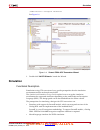
36 www.Xilinx.Com virtex-6 fpga gtx transceivers user guide ug366 (v2.5) january 17, 2011 chapter 1: transceiver and tool overview virtex-6 fpga gtx transceiver wizard the virtex-6 fpga gtx transceiver wizard is the preferred tool to generate a wrapper to instantiate a gtx transceiver primitive call...
Page 37: Simulation
Virtex-6 fpga gtx transceivers user guide www.Xilinx.Com 37 ug366 (v2.5) january 17, 2011 simulation /fpga features & design/io interfaces see figure 1-4 . 3. Double-click v6 gtx wizard to launch the wizard. Simulation functional description simulations using gtx transceivers have specific prerequis...
Page 38: Www.Bdtic.Com/xilinx
38 www.Xilinx.Com virtex-6 fpga gtx transceivers user guide ug366 (v2.5) january 17, 2011 chapter 1: transceiver and tool overview secureip models use a verilog standard. To use them in a vhdl design, a mixed- language simulator is required. The simulator must be capable of simulating vhdl and veril...
Page 39: Www.Bdtic.Com/xilinx
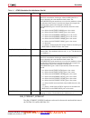
Virtex-6 fpga gtx transceivers user guide www.Xilinx.Com 39 ug366 (v2.5) january 17, 2011 simulation sim_gtxreset_speedup the sim_gtxreset_speedup attribute can be used to shorten the simulated lock time of the tx pma pll and the rx pma pll. Sim_rxrefclk_source 3-bit binary this attribute selects th...
Page 40: Www.Bdtic.Com/xilinx
40 www.Xilinx.Com virtex-6 fpga gtx transceivers user guide ug366 (v2.5) january 17, 2011 chapter 1: transceiver and tool overview if txoutclk or rxrecclk is used to generate clocks in the design, these clocks occasionally flatline while the gtx transceiver is locking. If an mmcm is used to divide t...
Page 41: Implementation
Virtex-6 fpga gtx transceivers user guide www.Xilinx.Com 41 ug366 (v2.5) january 17, 2011 implementation sim_version the sim_version attribute selects the simulation version to match different steppings of silicon. The default for this attribute is 1.0. Sim_tx_elec_idle_level the sim_tx_elec_idle_le...
Page 42: Www.Bdtic.Com/xilinx
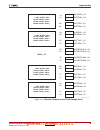
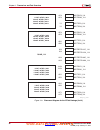
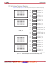
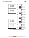
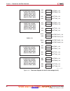
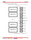
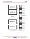
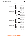
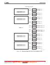
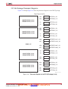
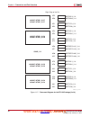
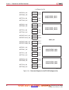
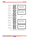
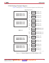
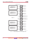
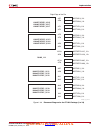
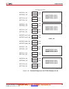
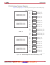
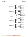
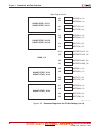
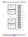
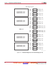
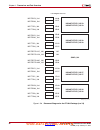
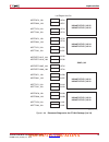
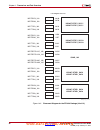
42 www.Xilinx.Com virtex-6 fpga gtx transceivers user guide ug366 (v2.5) january 17, 2011 chapter 1: transceiver and tool overview figure 1-5, page 42 through figure 1-23, page 60 provide the gtx transceiver position information for all available device and package combinations along with the pad nu...
Page 43: Www.Bdtic.Com/xilinx
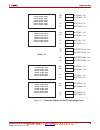
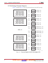
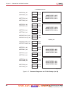
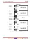
Virtex-6 fpga gtx transceivers user guide www.Xilinx.Com 43 ug366 (v2.5) january 17, 2011 implementation x-ref target - figure 1-6 figure 1-6: placement diagram for the ff484 package (2 of 2) lx75t: gtxe1_x0y 3 lx1 3 0t: gtxe1_x0y11 lx75t: gtxe1_x0y2 lx1 3 0t: gtxe1_x0y10 quad_114 lx75t: gtxe1_x0y1 ...
Page 44: Www.Bdtic.Com/xilinx
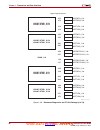
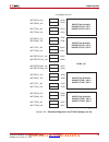
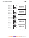
44 www.Xilinx.Com virtex-6 fpga gtx transceivers user guide ug366 (v2.5) january 17, 2011 chapter 1: transceiver and tool overview ff7 8 4 package placement diagrams figure 1-7 through figure 1-9 show the placement diagrams for the ff784 package. X-ref target - figure 1-7 figure 1-7: placement diagr...
Page 45: Www.Bdtic.Com/xilinx
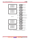
Virtex-6 fpga gtx transceivers user guide www.Xilinx.Com 45 ug366 (v2.5) january 17, 2011 implementation x-ref target - figure 1- 8 figure 1-8: placement diagram for the ff784 package (2 of 3) lx75t: gtxe1_x0y7 lx1 3 0t: gtxe1_x0y15 lx195t: gtxe1_x0y15 lx240t: gtxe1_x0y15 lx75t: gtxe1_x0y6 lx1 3 0t:...
Page 46: Www.Bdtic.Com/xilinx
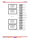
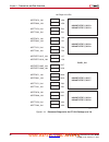
46 www.Xilinx.Com virtex-6 fpga gtx transceivers user guide ug366 (v2.5) january 17, 2011 chapter 1: transceiver and tool overview x-ref target - figure 1-9 figure 1-9: placement diagram for the ff784 package (3 of 3) lx75t: gtxe1_x0y 3 lx1 3 0t: gtxe1_x0y11 lx195t: gtxe1_x0y11 lx240t: gtxe1_x0y11 l...
Page 47: Www.Bdtic.Com/xilinx
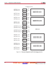
Virtex-6 fpga gtx transceivers user guide www.Xilinx.Com 47 ug366 (v2.5) january 17, 2011 implementation ff1156 package placement diagrams figure 1-10 through figure 1-14 show the placement diagrams for the ff1156 package. X-ref target - figure 1-10 figure 1-10: placement diagram for the ff1156 pack...
Page 48: Www.Bdtic.Com/xilinx
48 www.Xilinx.Com virtex-6 fpga gtx transceivers user guide ug366 (v2.5) january 17, 2011 chapter 1: transceiver and tool overview x-ref target - figure 1-11 figure 1-11: placement diagram for the ff1156 package (2 of 5) lx1 3 0t: gtxe1_x0y15 lx195t: gtxe1_x0y15 lx240t: gtxe1_x0y15 lx 3 65t: gtxe1_x...
Page 49: Www.Bdtic.Com/xilinx
Virtex-6 fpga gtx transceivers user guide www.Xilinx.Com 49 ug366 (v2.5) january 17, 2011 implementation x-ref target - figure 1-12 figure 1-12: placement diagram for the ff1156 package (3 of 5) lx1 3 0t: gtxe1_x0y11 lx195t: gtxe1_x0y11 lx240t: gtxe1_x0y11 lx 3 65t: gtxe1_x0y11 s x 3 15t: gtxe1_x0y1...
Page 50: Www.Bdtic.Com/xilinx
50 www.Xilinx.Com virtex-6 fpga gtx transceivers user guide ug366 (v2.5) january 17, 2011 chapter 1: transceiver and tool overview x-ref target - figure 1-13 figure 1-13: placement diagram for the ff1156 package (4 of 5) lx1 3 0t: gtxe1_x0y7 lx195t: gtxe1_x0y7 lx240t: gtxe1_x0y7 lx 3 65t: gtxe1_x0y7...
Page 51: Www.Bdtic.Com/xilinx
Virtex-6 fpga gtx transceivers user guide www.Xilinx.Com 51 ug366 (v2.5) january 17, 2011 implementation x-ref target - figure 1-14 figure 1-14: placement diagram for the ff1156 package (5 of 5) lx1 3 0t: gtxe1_x0y 3 lx195t: gtxe1_x0y 3 lx240t: gtxe1_x0y 3 lx 3 65t: gtxe1_x0y 3 s x 3 15t: gtxe1_x0y ...
Page 52: Www.Bdtic.Com/xilinx
52 www.Xilinx.Com virtex-6 fpga gtx transceivers user guide ug366 (v2.5) january 17, 2011 chapter 1: transceiver and tool overview ff1759 package placement diagrams figure 1-15 through figure 1-23 show the placement diagrams for the ff1759 package. X-ref target - figure 1-15 figure 1-15: placement d...
Page 53: Www.Bdtic.Com/xilinx
Virtex-6 fpga gtx transceivers user guide www.Xilinx.Com 53 ug366 (v2.5) january 17, 2011 implementation x-ref target - figure 1-16 figure 1-16: placement diagram for the ff1759 package (2 of 9) lx240t: gtxe1_x0y2 3 lx 3 65t: gtxe1_x0y2 3 lx550t: gtxe1_x0y 3 1 s x 3 15t: gtxe1_x0y2 3 s x475t: gtxe1_...
Page 54: Www.Bdtic.Com/xilinx
54 www.Xilinx.Com virtex-6 fpga gtx transceivers user guide ug366 (v2.5) january 17, 2011 chapter 1: transceiver and tool overview x-ref target - figure 1-17 figure 1-17: placement diagram for the ff1759 package (3 of 9) lx240t: gtxe1_x0y19 lx 3 65t: gtxe1_x0y19 lx550t: gtxe1_x0y27 s x 3 15t: gtxe1_...
Page 55: Www.Bdtic.Com/xilinx
Virtex-6 fpga gtx transceivers user guide www.Xilinx.Com 55 ug366 (v2.5) january 17, 2011 implementation x-ref target - figure 1-1 8 figure 1-18: placement diagram for the ff1759 package (4 of 9) lx240t: gtxe1_x0y15 lx 3 65t: gtxe1_x0y15 lx550t: gtxe1_x0y2 3 s x 3 15t: gtxe1_x0y15 s x475t: gtxe1_x0y...
Page 56: Www.Bdtic.Com/xilinx
56 www.Xilinx.Com virtex-6 fpga gtx transceivers user guide ug366 (v2.5) january 17, 2011 chapter 1: transceiver and tool overview x-ref target - figure 1-19 figure 1-19: placement diagram for the ff1759 package (5 of 9) lx240t: gtxe1_x0y11 lx 3 65t: gtxe1_x0y11 lx550t: gtxe1_x0y19 s x 3 15t: gtxe1_...
Page 57: Www.Bdtic.Com/xilinx
Virtex-6 fpga gtx transceivers user guide www.Xilinx.Com 57 ug366 (v2.5) january 17, 2011 implementation x-ref target - figure 1-20 figure 1-20: placement diagram for the ff1759 package (6 of 9) lx240t: gtxe1_x0y7 lx 3 65t: gtxe1_x0y7 lx550t: gtxe1_x0y15 s x 3 15t: gtxe1_x0y7 s x475t: gtxe1_x0y15 lx...
Page 58: Www.Bdtic.Com/xilinx
58 www.Xilinx.Com virtex-6 fpga gtx transceivers user guide ug366 (v2.5) january 17, 2011 chapter 1: transceiver and tool overview x-ref target - figure 1-21 figure 1-21: placement diagram for the ff1759 package (7 of 9) lx240t: gtxe1_x0y 3 lx 3 65t: gtxe1_x0y 3 lx550t: gtxe1_x0y11 s x 3 15t: gtxe1_...
Page 59: Www.Bdtic.Com/xilinx
Virtex-6 fpga gtx transceivers user guide www.Xilinx.Com 59 ug366 (v2.5) january 17, 2011 implementation x-ref target - figure 1-22 figure 1-22: placement diagram for the ff1759 package (8 of 9) lx240t: not available lx 3 65t: not available lx550t: gtxe1_x0y7 s x 3 15t: not available s x475t: gtxe1_...
Page 60: Www.Bdtic.Com/xilinx
60 www.Xilinx.Com virtex-6 fpga gtx transceivers user guide ug366 (v2.5) january 17, 2011 chapter 1: transceiver and tool overview x-ref target - figure 1-23 figure 1-23: placement diagram for the ff1759 package (9 of 9) lx240t: not available lx 3 65t: not available lx550t: gtxe1_x0y 3 s x 3 15t: no...
Page 61: Www.Bdtic.Com/xilinx
Virtex-6 fpga gtx transceivers user guide www.Xilinx.Com 61 ug366 (v2.5) january 17, 2011 implementation ff1154 package placement diagrams figure 1-24 through figure 1-35 show the placement diagrams for the ff1154 package. X-ref target - figure 1-24 figure 1-24: placement diagram for the ff1154 pack...
Page 62: Www.Bdtic.Com/xilinx
62 www.Xilinx.Com virtex-6 fpga gtx transceivers user guide ug366 (v2.5) january 17, 2011 chapter 1: transceiver and tool overview x-ref target - figure 1-25 figure 1-25: placement diagram for the ff1154 package (2 of 12) hx250t:gtxe1_x1y19 hx380t:gtxe1_x1y19 hx250t:gtxe1_x1y18 hx380t:gtxe1_x1y18 hx...
Page 63: Www.Bdtic.Com/xilinx
Virtex-6 fpga gtx transceivers user guide www.Xilinx.Com 63 ug366 (v2.5) january 17, 2011 implementation x-ref target - figure 1-26 figure 1-26: placement diagram for the ff1154 package (3 of 12) hx250t:gtxe1_x1y15 hx380t:gtxe1_x1y15 hx250t:gtxe1_x1y14 hx380t:gtxe1_x1y14 hx250t:gtxe1_x1y13 hx380t:gt...
Page 64: Www.Bdtic.Com/xilinx
64 www.Xilinx.Com virtex-6 fpga gtx transceivers user guide ug366 (v2.5) january 17, 2011 chapter 1: transceiver and tool overview x-ref target - figure 1-27 figure 1-27: placement diagram for the ff1154 package (4 of 12) hx250t:gtxe1_x1y11 hx380t:gtxe1_x1y11 hx250t:gtxe1_x1y10 hx380t:gtxe1_x1y10 hx...
Page 65: Www.Bdtic.Com/xilinx
Virtex-6 fpga gtx transceivers user guide www.Xilinx.Com 65 ug366 (v2.5) january 17, 2011 implementation x-ref target - figure 1-2 8 figure 1-28: placement diagram for the ff1154 package (5 of 12) hx250t:gtxe1_x1y7 hx380t:gtxe1_x1y7 hx250t:gtxe1_x1y6 hx380t:gtxe1_x1y6 hx250t:gtxe1_x1y5 hx380t:gtxe1_...
Page 66: Www.Bdtic.Com/xilinx
66 www.Xilinx.Com virtex-6 fpga gtx transceivers user guide ug366 (v2.5) january 17, 2011 chapter 1: transceiver and tool overview x-ref target - figure 1-29 figure 1-29: placement diagram for the ff1154 package (6 of 12) hx250t:gtxe1_x1y3 hx380t:gtxe1_x1y3 hx250t:gtxe1_x1y2 hx380t:gtxe1_x1y2 hx250t...
Page 67: Www.Bdtic.Com/xilinx
Virtex-6 fpga gtx transceivers user guide www.Xilinx.Com 67 ug366 (v2.5) january 17, 2011 implementation x-ref target - figure 1-30 figure 1-30: placement diagram for the ff1154 package (7 of 12) hx250t:gtxe1_x0y23 hx380t:gtxe1_x0y23 hx250t:gtxe1_x0y22 hx380t:gtxe1_x0y22 hx250t:gtxe1_x0y21 hx380t:gt...
Page 68: Www.Bdtic.Com/xilinx
68 www.Xilinx.Com virtex-6 fpga gtx transceivers user guide ug366 (v2.5) january 17, 2011 chapter 1: transceiver and tool overview x-ref target - figure 1-31 figure 1-31: placement diagram for the ff1154 package (8 of 12) hx250t:gtxe1_x0y19 hx380t:gtxe1_x0y19 hx250t:gtxe1_x0y18 hx380t:gtxe1_x0y18 hx...
Page 69: Www.Bdtic.Com/xilinx
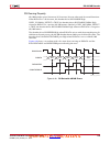
Virtex-6 fpga gtx transceivers user guide www.Xilinx.Com 69 ug366 (v2.5) january 17, 2011 implementation x-ref target - figure 1-32 figure 1-32: placement diagram for the ff1154 package (9 of 12) hx250t:gtxe1_x0y15 hx380t:gtxe1_x0y15 hx250t:gtxe1_x0y14 hx380t:gtxe1_x0y14 hx250t:gtxe1_x0y13 hx380t:gt...
Page 70: Www.Bdtic.Com/xilinx
70 www.Xilinx.Com virtex-6 fpga gtx transceivers user guide ug366 (v2.5) january 17, 2011 chapter 1: transceiver and tool overview x-ref target - figure 1-33 figure 1-33: placement diagram for the ff1154 package (10 of 12) hx250t:gtxe1_x0y11 hx380t:gtxe1_x0y11 hx250t:gtxe1_x0y10 hx380t:gtxe1_x0y10 h...
Page 71: Www.Bdtic.Com/xilinx
Virtex-6 fpga gtx transceivers user guide www.Xilinx.Com 71 ug366 (v2.5) january 17, 2011 implementation x-ref target - figure 1-34 figure 1-34: placement diagram for the ff1154 package (11 of 12) hx250t:gtxe1_x0y7 hx380t:gtxe1_x0y7 hx250t:gtxe1_x0y6 hx380t:gtxe1_x0y6 hx250t:gtxe1_x0y5 hx380t:gtxe1_...
Page 72: Www.Bdtic.Com/xilinx
72 www.Xilinx.Com virtex-6 fpga gtx transceivers user guide ug366 (v2.5) january 17, 2011 chapter 1: transceiver and tool overview x-ref target - figure 1-35 figure 1-35: placement diagram for the ff1154 package (12 of 12) hx250t:gtxe1_x0y3 hx380t:gtxe1_x0y3 hx250t:gtxe1_x0y2 hx380t:gtxe1_x0y2 hx250...
Page 73: Www.Bdtic.Com/xilinx
Virtex-6 fpga gtx transceivers user guide www.Xilinx.Com 73 ug366 (v2.5) january 17, 2011 implementation ff1155 package placement diagrams figure 1-36 through figure 1-41 show the placement diagrams for the ff1155 package. X-ref target - figure 1-36 figure 1-36: placement diagram for the ff1155 pack...
Page 74: Www.Bdtic.Com/xilinx
74 www.Xilinx.Com virtex-6 fpga gtx transceivers user guide ug366 (v2.5) january 17, 2011 chapter 1: transceiver and tool overview x-ref target - figure 1-37 figure 1-37: placement diagram for the ff1155 package (2 of 6) hx255t:gtxe1_x1y7 hx380t:gtxe1_x1y7 hx255t:gtxe1_x1y6 hx380t:gtxe1_x1y6 hx2555t...
Page 75: Www.Bdtic.Com/xilinx
Virtex-6 fpga gtx transceivers user guide www.Xilinx.Com 75 ug366 (v2.5) january 17, 2011 implementation x-ref target - figure 1-3 8 figure 1-38: placement diagram for the ff1155 package (3 of 6) hx255t:gtxe1_x1y3 hx380t:gtxe1_x1y3 hx255t:gtxe1_x1y2 hx380t:gtxe1_x1y2 hx255t:gtxe1_x1y1 hx380t:gtxe1_x...
Page 76: Www.Bdtic.Com/xilinx
76 www.Xilinx.Com virtex-6 fpga gtx transceivers user guide ug366 (v2.5) january 17, 2011 chapter 1: transceiver and tool overview x-ref target - figure 1-39 figure 1-39: placement diagram for the ff1155 package (4 of 6) hx255t:gtxe1_x0y11 hx380t:gtxe1_x0y11 hx255t:gtxe1_x0y10 hx380t:gtxe1_x0y10 hx2...
Page 77: Www.Bdtic.Com/xilinx
Virtex-6 fpga gtx transceivers user guide www.Xilinx.Com 77 ug366 (v2.5) january 17, 2011 implementation x-ref target - figure 1-40 figure 1-40: placement diagram for the ff1155 package (5 of 6) hx255t:gtxe1_x0y7 hx380t:gtxe1_x0y7 hx255t:gtxe1_x0y6 hx380t:gtxe1_x0y6 hx255t:gtxe1_x0y5 hx380t:gtxe1_x0...
Page 78: Www.Bdtic.Com/xilinx
78 www.Xilinx.Com virtex-6 fpga gtx transceivers user guide ug366 (v2.5) january 17, 2011 chapter 1: transceiver and tool overview x-ref target - figure 1-41 figure 1-41: placement diagram for the ff1155 package (6 of 6) hx255t:gtxe1_x0y3 hx380t:gtxe1_x0y3 hx255t:gtxe1_x0y2 hx380t:gtxe1_x0y2 hx255t:...
Page 79: Www.Bdtic.Com/xilinx
Virtex-6 fpga gtx transceivers user guide www.Xilinx.Com 79 ug366 (v2.5) january 17, 2011 implementation ff1923 package placement diagrams figure 1-42 through figure 1-51 show the placement diagrams for the ff1923 package. X-ref target - figure 1-42 figure 1-42: placement diagram for the ff1923 pack...
Page 80: Www.Bdtic.Com/xilinx
80 www.Xilinx.Com virtex-6 fpga gtx transceivers user guide ug366 (v2.5) january 17, 2011 chapter 1: transceiver and tool overview x-ref target - figure 1-43 figure 1-43: placement diagram for the ff1923 package (2 of 10) hx255t:gtxe1_x1y7 hx380t:gtxe1_x1y11 hx565t:gtxe1_x1y11 hx255t:gtxe1_x1y6 hx38...
Page 81: Www.Bdtic.Com/xilinx
Virtex-6 fpga gtx transceivers user guide www.Xilinx.Com 81 ug366 (v2.5) january 17, 2011 implementation x-ref target - figure 1-44 figure 1-44: placement diagram for the ff1923 package (3 of 10) hx255t:gtxe1_x1y3 hx380t:gtxe1_x1y7 hx565t:gtxe1_x1y7 hx255t:gtxe1_x1y2 hx380t:gtxe1_x1y6 hx565t:gtxe1_x...
Page 82: Www.Bdtic.Com/xilinx
82 www.Xilinx.Com virtex-6 fpga gtx transceivers user guide ug366 (v2.5) january 17, 2011 chapter 1: transceiver and tool overview x-ref target - figure 1-45 figure 1-45: placement diagram for the ff1923 package (4 of 10) hx255t:not available hx380t:gtxe1_x1y3 hx565t:gtxe1_x1y3 hx255t:not available ...
Page 83: Www.Bdtic.Com/xilinx
Virtex-6 fpga gtx transceivers user guide www.Xilinx.Com 83 ug366 (v2.5) january 17, 2011 implementation x-ref target - figure 1-46 figure 1-46: placement diagram for the ff1923 package (5 of 10) u38 u37 v44 v43 v40 v39 w42 w41 t35 t36 v35 v36 w38 w37 y44 y43 y40 y39 aa42 aa41 mgttxp0_105 mgttxn0_10...
Page 84: Www.Bdtic.Com/xilinx
84 www.Xilinx.Com virtex-6 fpga gtx transceivers user guide ug366 (v2.5) january 17, 2011 chapter 1: transceiver and tool overview x-ref target - figure 1-47 figure 1-47: placement diagram for the ff1923 package (6 of 10) aa38 aa37 ab44 ab43 ab40 ab39 ac42 ac41 y35 y36 ab35 ab36 ac38 ac37 ad44 ad43 ...
Page 85: Www.Bdtic.Com/xilinx
Virtex-6 fpga gtx transceivers user guide www.Xilinx.Com 85 ug366 (v2.5) january 17, 2011 implementation x-ref target - figure 1-4 8 figure 1-48: placement diagram for the ff1923 package (7 of 10) ae38 ae37 af44 af43 af40 af39 ag42 ag41 ad35 ad36 af35 af36 ag38 ag37 ah44 ah43 ah40 ah39 aj42 aj41 ug3...
Page 86: Www.Bdtic.Com/xilinx
86 www.Xilinx.Com virtex-6 fpga gtx transceivers user guide ug366 (v2.5) january 17, 2011 chapter 1: transceiver and tool overview x-ref target - figure 1-49 figure 1-49: placement diagram for the ff1923 package (8 of 10) ak40 ak39 ak44 ak43 aj38 aj37 al42 al41 ah35 ah36 an37 an38 am40 am39 am44 am4...
Page 87: Www.Bdtic.Com/xilinx
Virtex-6 fpga gtx transceivers user guide www.Xilinx.Com 87 ug366 (v2.5) january 17, 2011 implementation x-ref target - figure 1-50 figure 1-50: placement diagram for the ff1923 package (9 of 10) ap40 ap39 ap44 ap43 at40 at39 ar42 ar41 ar37 ar38 au37 au38 av40 av39 at44 at43 ay40 ay39 au42 au41 ug36...
Page 88: Www.Bdtic.Com/xilinx
88 www.Xilinx.Com virtex-6 fpga gtx transceivers user guide ug366 (v2.5) january 17, 2011 chapter 1: transceiver and tool overview x-ref target - figure 1-51 figure 1-51: placement diagram for the ff1923 package (10 of 10) ba42 ba41 av44 av43 bb40 bb39 aw42 aw41 aw37 aw38 ba37 ba38 bc42 bc41 ay44 ay...
Page 89: Www.Bdtic.Com/xilinx
Virtex-6 fpga gtx transceivers user guide www.Xilinx.Com 89 ug366 (v2.5) january 17, 2011 implementation ff1924 package placement diagrams figure 1-42 through figure 1-51 show the placement diagrams for the ff1924 package. X-ref target - figure 1-52 figure 1-52: placement diagram for the ff1924 pack...
Page 90: Www.Bdtic.Com/xilinx
90 www.Xilinx.Com virtex-6 fpga gtx transceivers user guide ug366 (v2.5) january 17, 2011 chapter 1: transceiver and tool overview x-ref target - figure 1-53 figure 1-53: placement diagram for the ff1924 package (2 of 12) hx380t:gtxe1_x1y19 hx565t:gtxe1_x1y19 hx380t:gtxe1_x1y18 hx565t:gtxe1_x1y18 hx...
Page 91: Www.Bdtic.Com/xilinx
Virtex-6 fpga gtx transceivers user guide www.Xilinx.Com 91 ug366 (v2.5) january 17, 2011 implementation x-ref target - figure 1-54 figure 1-54: placement diagram for the ff1924 package (3 of 12) hx380t:gtxe1_x1y15 hx565t:gtxe1_x1y15 hx380t:gtxe1_x1y14 hx565t:gtxe1_x1y14 hx380t:gtxe1_x1y13 hx565t:gt...
Page 92: Www.Bdtic.Com/xilinx
92 www.Xilinx.Com virtex-6 fpga gtx transceivers user guide ug366 (v2.5) january 17, 2011 chapter 1: transceiver and tool overview x-ref target - figure 1-55 figure 1-55: placement diagram for the ff1924 package (4 of 12) hx380t:gtxe1_x1y11 hx565t:gtxe1_x1y11 hx380t:gtxe1_x1y10 hx565t:gtxe1_x1y10 hx...
Page 93: Www.Bdtic.Com/xilinx
Virtex-6 fpga gtx transceivers user guide www.Xilinx.Com 93 ug366 (v2.5) january 17, 2011 implementation x-ref target - figure 1-56 figure 1-56: placement diagram for the ff1924 package (5 of 12) hx380t:gtxe1_x1y7 hx565t:gtxe1_x1y7 hx380t:gtxe1_x1y6 hx565t:gtxe1_x1y6 hx380t:gtxe1_x1y5 hx565t:gtxe1_x...
Page 94: Www.Bdtic.Com/xilinx
94 www.Xilinx.Com virtex-6 fpga gtx transceivers user guide ug366 (v2.5) january 17, 2011 chapter 1: transceiver and tool overview x-ref target - figure 1-57 figure 1-57: placement diagram for the ff1924 package (6 of 12) hx380t:gtxe1_x1y3 hx565t:gtxe1_x1y3 hx380t:gtxe1_x1y2 hx565t:gtxe1_x1y2 hx380t...
Page 95: Www.Bdtic.Com/xilinx
Virtex-6 fpga gtx transceivers user guide www.Xilinx.Com 95 ug366 (v2.5) january 17, 2011 implementation x-ref target - figure 1-5 8 figure 1-58: placement diagram for the ff1924 package (7 of 12) quad_105 u38 u37 v44 v43 v40 v39 w42 w41 t35 t36 v35 v36 w38 w37 y44 y43 y40 y39 aa42 aa42 mgttxp0_105 ...
Page 96: Www.Bdtic.Com/xilinx
96 www.Xilinx.Com virtex-6 fpga gtx transceivers user guide ug366 (v2.5) january 17, 2011 chapter 1: transceiver and tool overview x-ref target - figure 1-59 figure 1-59: placement diagram for the ff1924 package (8 of 12) quad_104 aa38 aa37 ab44 ab43 ab40 ab39 ac42 ac41 y35 y36 ab35 ab36 ac38 ac37 a...
Page 97: Www.Bdtic.Com/xilinx
Virtex-6 fpga gtx transceivers user guide www.Xilinx.Com 97 ug366 (v2.5) january 17, 2011 implementation x-ref target - figure 1-60 figure 1-60: placement diagram for the ff1924 package (9 of 12) quad_103 ae38 ae37 af44 af43 af40 af39 ag42 ag41 ad35 ad36 af35 af36 ag38 ag37 ah44 ah43 ah40 ah39 aj42 ...
Page 98: Www.Bdtic.Com/xilinx
98 www.Xilinx.Com virtex-6 fpga gtx transceivers user guide ug366 (v2.5) january 17, 2011 chapter 1: transceiver and tool overview x-ref target - figure 1-61 figure 1-61: placement diagram for the ff1924 package (10 of 12) quad_102 ak40 ak39 ak44 ak43 aj38 aj37 al42 al41 ah35 ah36 an37 an38 am40 am3...
Page 99: Www.Bdtic.Com/xilinx
Virtex-6 fpga gtx transceivers user guide www.Xilinx.Com 99 ug366 (v2.5) january 17, 2011 implementation x-ref target - figure 1-62 figure 1-62: placement diagram for the ff1924 package (11 of 12) quad_101 ap40 ap39 ap44 ap43 at40 at39 ar42 ar41 ar37 ar38 au37 au38 av40 av39 at44 at43 ay40 ay39 au42...
Page 100: Www.Bdtic.Com/xilinx
100 www.Xilinx.Com virtex-6 fpga gtx transceivers user guide ug366 (v2.5) january 17, 2011 chapter 1: transceiver and tool overview x-ref target - figure 1-63 figure 1-63: placement diagram for the ff1924 package (12 of 12) quad_100 ba42 ba41 av44 av43 bb40 bb39 aw42 aw41 aw37 aw36 ba37 ba38 bc42 bc...
Page 101: Shared Transceiver Features
Virtex-6 fpga gtx transceivers user guide www.Xilinx.Com 101 ug366 (v2.5) january 17, 2011 chapter 2 shared transceiver features reference clock input structure functional description the reference clock input structure is illustrated in figure 2-1 . The input is terminated internally with 50 on eac...
Page 102: Reference Clock Selection
102 www.Xilinx.Com virtex-6 fpga gtx transceivers user guide ug366 (v2.5) january 17, 2011 chapter 2: shared transceiver features table 2-2 defines the attributes in the ibufds_gtxe1 software primitive that configure the reference clock input. Use modes: reference clock termination the reference clo...
Page 103: Www.Bdtic.Com/xilinx
Virtex-6 fpga gtx transceivers user guide www.Xilinx.Com 103 ug366 (v2.5) january 17, 2011 reference clock selection document describes the reference clocking architecture of the virtex-6 fpga gtx transceivers. Reference clock features include: • clock routing for north and south bound clocks. • clo...
Page 104: Www.Bdtic.Com/xilinx
104 www.Xilinx.Com virtex-6 fpga gtx transceivers user guide ug366 (v2.5) january 17, 2011 chapter 2: shared transceiver features x-ref target - figure 2-2 figure 2-2: conceptual view of gtx transceiver reference clocking ug 3 66_c2_01_051509 gtx2 gtx1 mgtrefclk0 q (n+1) nor thclk1 q (n+1) nor thclk...
Page 105: Www.Bdtic.Com/xilinx
Virtex-6 fpga gtx transceivers user guide www.Xilinx.Com 105 ug366 (v2.5) january 17, 2011 reference clock selection figure 2-3 shows the detailed view of the reference clock multiplexer structure within a single gtxe1 primitive. The txpllrefseldy and rxpllrefseldy ports are required when multiple r...
Page 106: Www.Bdtic.Com/xilinx
106 www.Xilinx.Com virtex-6 fpga gtx transceivers user guide ug366 (v2.5) january 17, 2011 chapter 2: shared transceiver features within the quad. In addition, they can be routed to the gtx transceivers in the north or south neighboring quads using the dedicated reference clock routing shown in figu...
Page 107: Www.Bdtic.Com/xilinx
Virtex-6 fpga gtx transceivers user guide www.Xilinx.Com 107 ug366 (v2.5) january 17, 2011 reference clock selection table 2-5 defines the gtx clocking attributes. Rxpllrefseldy[2:0] in async receiver pll reference clock dynamic selection. Set to 000 when one reference clock is used. When multiple r...
Page 108: Www.Bdtic.Com/xilinx
108 www.Xilinx.Com virtex-6 fpga gtx transceivers user guide ug366 (v2.5) january 17, 2011 chapter 2: shared transceiver features single external reference clock use model each quad has two dedicated differential reference clock inputs (mgtrefclk0[p/n] or mgtrefclk1[p/n]) that can be connected to ex...
Page 109: Www.Bdtic.Com/xilinx
Virtex-6 fpga gtx transceivers user guide www.Xilinx.Com 109 ug366 (v2.5) january 17, 2011 reference clock selection note: the ibufds_gtxe1 diagram in figure 2-5 is a simplification. The output port odiv2 is left floating, and the input port ceb is set to logic 0. The xilinx implementation tools mak...
Page 110: Www.Bdtic.Com/xilinx
110 www.Xilinx.Com virtex-6 fpga gtx transceivers user guide ug366 (v2.5) january 17, 2011 chapter 2: shared transceiver features 3. The total number of quads sourced by an external clock pin pair (mgtrefclkn/mgtrefclkp) must not exceed 3 quads (or 12 gtx transceivers). The maximum number of gtx tra...
Page 111: Www.Bdtic.Com/xilinx
Virtex-6 fpga gtx transceivers user guide www.Xilinx.Com 111 ug366 (v2.5) january 17, 2011 reference clock selection note: the ibufds_gtxe1 diagram in figure 2-6 is a simplification. The output port odiv2 is left floating, and the input port ceb is set to logic 0. The user constraints file (ucf) can...
Page 112: Www.Bdtic.Com/xilinx
112 www.Xilinx.Com virtex-6 fpga gtx transceivers user guide ug366 (v2.5) january 17, 2011 chapter 2: shared transceiver features the flexibility of the reference clock selection architecture allows each transceiver within a quad to have access to the dedicated reference clocks from the quad immedia...
Page 113: Pll
Virtex-6 fpga gtx transceivers user guide www.Xilinx.Com 113 ug366 (v2.5) january 17, 2011 pll for multi-rate designs that require the reference clock source to be changed on the fly, the txpllrefseldy and rxpllrefseldy ports are used to dynamically select the reference clock source. When the select...
Page 114: Www.Bdtic.Com/xilinx
114 www.Xilinx.Com virtex-6 fpga gtx transceivers user guide ug366 (v2.5) january 17, 2011 chapter 2: shared transceiver features the pll input clock selection is described in reference clock selection, page 102 . The pll outputs feed the tx and rx clock divider blocks, which control the generation ...
Page 115: Www.Bdtic.Com/xilinx
Virtex-6 fpga gtx transceivers user guide www.Xilinx.Com 115 ug366 (v2.5) january 17, 2011 pll the virtex-6 fpga gtx transceiver allows the n1 divider to be set independently from the pcs internal datapath width. This allows additional flexibility in reference clock selection. Ports and attributes t...
Page 116: Www.Bdtic.Com/xilinx
116 www.Xilinx.Com virtex-6 fpga gtx transceivers user guide ug366 (v2.5) january 17, 2011 chapter 2: shared transceiver features tx_tdcc_cfg 2-bit binary reserved. Use only recommended values from the virtex-6 fpga gtx transceiver wizard. Txpll_com_cfg rxpll_com_cfg 24-bit hex reserved. Use only re...
Page 117: Www.Bdtic.Com/xilinx
Virtex-6 fpga gtx transceivers user guide www.Xilinx.Com 117 ug366 (v2.5) january 17, 2011 pll pll settings for common protocols table 2-10 shows example pll divider settings for several standard protocols. Rx_clk25_divider tx_clk25_divider integer this attribute is set to get an internal clock for ...
Page 118: Www.Bdtic.Com/xilinx
118 www.Xilinx.Com virtex-6 fpga gtx transceivers user guide ug366 (v2.5) january 17, 2011 chapter 2: shared transceiver features fibre channel (multi-rate) 4.25 20b 2.125 212.5 5 2 1 1 2.125 20b 2.125 212.5 5 2 2 1 1.0625 20b 2.125 212.5 5 2 4 1 xaui 3.125 20b 1.5625 156.25 5 2 1 1 gige 1.25 20b 2....
Page 119: Www.Bdtic.Com/xilinx
Virtex-6 fpga gtx transceivers user guide www.Xilinx.Com 119 ug366 (v2.5) january 17, 2011 pll some protocols are shown twice as a single-rate configuration and a multi-rate configuration. In single-rate configurations, only one line rate is required, and the reference clock is optimized for that pa...
Page 120: Power Down
120 www.Xilinx.Com virtex-6 fpga gtx transceivers user guide ug366 (v2.5) january 17, 2011 chapter 2: shared transceiver features power down functional description the gtx transceiver supports a range of power-down modes. These modes support both generic power management capabilities as well as thos...
Page 121: Www.Bdtic.Com/xilinx
Virtex-6 fpga gtx transceivers user guide www.Xilinx.Com 121 ug366 (v2.5) january 17, 2011 power down generic power-down capabilities the gtx transceiver provides several power-down features that can be used in a wide variety of applications. Table 2-13 summarizes these capabilities. Table 2-12: pow...
Page 122: Www.Bdtic.Com/xilinx
122 www.Xilinx.Com virtex-6 fpga gtx transceivers user guide ug366 (v2.5) january 17, 2011 chapter 2: shared transceiver features pll power down to activate the pll power-down mode, the active-high txpllpowerdown or rxpllpower down signal is asserted. When either pllpowerdown is asserted, the corres...
Page 123: Loopback
Virtex-6 fpga gtx transceivers user guide www.Xilinx.Com 123 ug366 (v2.5) january 17, 2011 loopback • rxpllpowerdown must be tied low. • rxpowerdown[0] and rxpowerdown[1] must be tied low. Refer to rx buffer bypass, page 231 for more information. Power-down features for pci express operation the gtx...
Page 124: Www.Bdtic.Com/xilinx
124 www.Xilinx.Com virtex-6 fpga gtx transceivers user guide ug366 (v2.5) january 17, 2011 chapter 2: shared transceiver features and then compared to check for errors. Figure 2-10 illustrates a loopback test configuration with four different loopback modes. Loopback test modes fall into two broad c...
Page 125: Acjtag
Virtex-6 fpga gtx transceivers user guide www.Xilinx.Com 125 ug366 (v2.5) january 17, 2011 acjtag table 2-17 defines the loopback attributes. Acjtag functional description the virtex-6 fpga gtx transceiver supports acjtag, as specified by ieee std 1149.6. To ensure reliable acjtag operation, the gtx...
Page 126: Www.Bdtic.Com/xilinx
126 www.Xilinx.Com virtex-6 fpga gtx transceivers user guide ug366 (v2.5) january 17, 2011 chapter 2: shared transceiver features ports and attributes table 2-18 defines the drp ports. There are no drp attributes. Note: attributes that have an impact on the entire quad (the cluster of four gtx trans...
Page 127: Transmitter
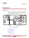
Virtex-6 fpga gtx transceivers user guide www.Xilinx.Com 127 ug366 (v2.5) january 17, 2011 chapter 3 transmitter tx overview this chapter shows how to configure and use each of the functional blocks inside the gtx transmitter (tx). Each gtx transceiver includes an independent transmitter, which cons...
Page 128: Fpga Tx Interface
128 www.Xilinx.Com virtex-6 fpga gtx transceivers user guide ug366 (v2.5) january 17, 2011 chapter 3: transmitter 8. Tx oversampling, page 166 9. Tx polarity control, page 166 10. Tx fabric clock output control, page 167 11. Tx configurable driver, page 172 12. Tx receiver detect support for pci exp...
Page 129: Www.Bdtic.Com/xilinx
Virtex-6 fpga gtx transceivers user guide www.Xilinx.Com 129 ug366 (v2.5) january 17, 2011 fpga tx interface when the 8b/10b encoder is bypassed and the tx_data_width is 10, 20, or 40, the txchardispmode and txchardispval ports are used to extend the txdata port from 8 to 10 bits, 16 to 20 bits, or ...
Page 130: Www.Bdtic.Com/xilinx
130 www.Xilinx.Com virtex-6 fpga gtx transceivers user guide ug366 (v2.5) january 17, 2011 chapter 3: transmitter these rules about the relationships between clocks must be observed for txusrclk and txusrclk2: • txusrclk and txusrclk2 must be positive-edge aligned, with as little skew as possible be...
Page 131: Www.Bdtic.Com/xilinx
Virtex-6 fpga gtx transceivers user guide www.Xilinx.Com 131 ug366 (v2.5) january 17, 2011 fpga tx interface table 3-6 defines the fpga tx interface attributes. Using txoutclk to drive the gtx tx figure 3-2 through figure 3-7 show different ways that fpga clock resources can be used to drive the par...
Page 132: Www.Bdtic.Com/xilinx
132 www.Xilinx.Com virtex-6 fpga gtx transceivers user guide ug366 (v2.5) january 17, 2011 chapter 3: transmitter refer to the virtex-6 fpga data sheet for the maximum clock frequency and jitter limitations of bufr. For details about placement constraints and restrictions on clocking resources (mmcm...
Page 133: Www.Bdtic.Com/xilinx
Virtex-6 fpga gtx transceivers user guide www.Xilinx.Com 133 ug366 (v2.5) january 17, 2011 fpga tx interface refer to the virtex-6 fpga data sheet for the maximum clock frequency and jitter limitations of bufr. For details about placement constraints and restrictions on clocking resources (mmcm, buf...
Page 134: Www.Bdtic.Com/xilinx
134 www.Xilinx.Com virtex-6 fpga gtx transceivers user guide ug366 (v2.5) january 17, 2011 chapter 3: transmitter for details about placement constraints and restrictions on clocking resources (mmcm, bufgctrl, ibufds_gtxe1, bufg, etc.), refer to the virtex-6 fpga clocking resources user guide . Txou...
Page 135: Www.Bdtic.Com/xilinx
Virtex-6 fpga gtx transceivers user guide www.Xilinx.Com 135 ug366 (v2.5) january 17, 2011 fpga tx interface for details about placement constraints and restrictions on clocking resources (mmcm, bufgctrl, ibufds_gtxe1, bufg, etc.), refer to the virtex-6 fpga clocking resources user guide . Txoutclk ...
Page 136: Tx Initialization
136 www.Xilinx.Com virtex-6 fpga gtx transceivers user guide ug366 (v2.5) january 17, 2011 chapter 3: transmitter for details about placement constraints and restrictions on clocking resources (mmcm, bufgctrl, ibufds_gtxe1, bufg, etc.), refer to the virtex-6 fpga clocking resources user guide . Tx i...
Page 137: Www.Bdtic.Com/xilinx
Virtex-6 fpga gtx transceivers user guide www.Xilinx.Com 137 ug366 (v2.5) january 17, 2011 tx initialization all reset ports described in this section initiate the internal transmitter state machines when driven high. The internal reset state machines are held in the reset state until these same res...
Page 138: Www.Bdtic.Com/xilinx
138 www.Xilinx.Com virtex-6 fpga gtx transceivers user guide ug366 (v2.5) january 17, 2011 chapter 3: transmitter notes relevant to figure 3-9 : • the minimum wait time from the rising edge of the txplllkdet/rxplllkdet signals to the first gtxtest[1] reset pulse is 1,024 clock cycles. • the minimum ...
Page 139: Www.Bdtic.Com/xilinx
Virtex-6 fpga gtx transceivers user guide www.Xilinx.Com 139 ug366 (v2.5) january 17, 2011 tx initialization gtx tx reset in response to completion of configuration figure 3-10 shows the gtx tx reset following the completion of configuration of a powered-up gtx transceiver. The same sequence is acti...
Page 140: Www.Bdtic.Com/xilinx
140 www.Xilinx.Com virtex-6 fpga gtx transceivers user guide ug366 (v2.5) january 17, 2011 chapter 3: transmitter notes relevant to figure 3-11 : 1. Gtxtest[1] is only required when the tx output clock divider, txpll_divsel_out, is set to /2 or /4. 2. The timing of the reset sequencer inside the gtx...
Page 141: Www.Bdtic.Com/xilinx
Virtex-6 fpga gtx transceivers user guide www.Xilinx.Com 141 ug366 (v2.5) january 17, 2011 tx initialization table 3-10 lists the recommended resets for various situations. Tx pma tx driver ✓ ✓ ✓ tx oob ✓ ✓ ✓ tx receiver detect for pcie designs ✓ ✓ ✓ tx pll ✓ ✓ ✓ ✓ piso ✓ ✓ ✓ loopback loopback paths...
Page 142: Www.Bdtic.Com/xilinx
142 www.Xilinx.Com virtex-6 fpga gtx transceivers user guide ug366 (v2.5) january 17, 2011 chapter 3: transmitter see tx buffer bypass, page 155 for details on the rate change procedure. After power-up and configuration the entire gtx tx is reset automatically after configuration-provided txpllpower...
Page 143: Tx 8B/10B Encoder
Virtex-6 fpga gtx transceivers user guide www.Xilinx.Com 143 ug366 (v2.5) january 17, 2011 tx 8b/10b encoder tx 8b/10b encoder functional description many protocols use 8b/10b encoding on outgoing data. 8b/10b is an industry-standard encoding scheme that trades two bits of overhead per byte for impr...
Page 144: Www.Bdtic.Com/xilinx
144 www.Xilinx.Com virtex-6 fpga gtx transceivers user guide ug366 (v2.5) january 17, 2011 chapter 3: transmitter k characters the 8b/10b table includes special characters (k characters) that are often used for control functions. To transmit txdata as a k character instead of regular data, the txcha...
Page 145: Www.Bdtic.Com/xilinx
Virtex-6 fpga gtx transceivers user guide www.Xilinx.Com 145 ug366 (v2.5) january 17, 2011 tx 8b/10b encoder table 3-12: tx encoder ports port dir clock domain description txbypass8b10b[3:0] in txusrclk2 txbypass8b10b controls the operation of the tx 8b/10b encoder on a per-byte basis. It is only ef...
Page 146: Tx Gearbox
146 www.Xilinx.Com virtex-6 fpga gtx transceivers user guide ug366 (v2.5) january 17, 2011 chapter 3: transmitter there are no tx encoder attributes. Enabling and disabling 8 b/10b encoding to enable the 8b/10b encoder, txenc8b10buse must be driven high. To disable the 8b/10b encoder on a given gtx ...
Page 147: Www.Bdtic.Com/xilinx
Virtex-6 fpga gtx transceivers user guide www.Xilinx.Com 147 ug366 (v2.5) january 17, 2011 tx gearbox table 3-14 defines the tx gearbox attributes. Enabling the tx gearbox to enable the tx gearbox for the gtx transceiver, the txgearbox_use attribute is set to true. Bit 2 of the gearbox_endec attribu...
Page 148: Www.Bdtic.Com/xilinx
148 www.Xilinx.Com virtex-6 fpga gtx transceivers user guide ug366 (v2.5) january 17, 2011 chapter 3: transmitter header of the second 66-bit block, and 12 data bits from the second 66-bit block. As shown in figure 3-13 , the header bits are serialized first followed by the data bits. Tx gearbox ope...
Page 149: Www.Bdtic.Com/xilinx
Virtex-6 fpga gtx transceivers user guide www.Xilinx.Com 149 ug366 (v2.5) january 17, 2011 tx gearbox external se q uence counter operating mode as shown in figure 3-14 , the external sequence counter operating mode uses the txsequence[6:0], txdata[31:0], and txheader[2:0] inputs. A binary counter m...
Page 150: Www.Bdtic.Com/xilinx
150 www.Xilinx.Com virtex-6 fpga gtx transceivers user guide ug366 (v2.5) january 17, 2011 chapter 3: transmitter figure 3-16 shows how a pause occurs at counter value 44 when using a 2-byte interface, external sequence counter mode, and 64b/67b encoding. The sequence of transmitting 64b/67b data fo...
Page 151: Www.Bdtic.Com/xilinx
Virtex-6 fpga gtx transceivers user guide www.Xilinx.Com 151 ug366 (v2.5) january 17, 2011 tx gearbox internal se q uence counter operating mode as shown in figure 3-17 , the internal sequence counter operating mode uses the txstartseq input and the txgearboxready output in addition to the txdata da...
Page 152: Www.Bdtic.Com/xilinx
152 www.Xilinx.Com virtex-6 fpga gtx transceivers user guide ug366 (v2.5) january 17, 2011 chapter 3: transmitter the sequence of transmitting data for the internal sequence counter mode is: 1. Hold txstartseq low. 2. Assert txreset and wait until the reset cycle is completed. 3. Txgearboxready goes...
Page 153: Tx Buffer
Virtex-6 fpga gtx transceivers user guide www.Xilinx.Com 153 ug366 (v2.5) january 17, 2011 tx buffer tx buffer functional description the gtx tx datapath has two internal parallel clock domains used in the pcs: the pma parallel clock domain (xclk) and the txusrclk domain. To transmit data, the xclk ...
Page 154: Www.Bdtic.Com/xilinx
154 www.Xilinx.Com virtex-6 fpga gtx transceivers user guide ug366 (v2.5) january 17, 2011 chapter 3: transmitter ports and attributes table 3-16 defines the tx buffer ports. Table 3-16 defines the tx buffer attributes. Using the tx buffer to use the tx buffer to resolve phase differences between th...
Page 155: Tx Buffer Bypass
Virtex-6 fpga gtx transceivers user guide www.Xilinx.Com 155 ug366 (v2.5) january 17, 2011 tx buffer bypass tx buffer bypass functional description bypassing the tx buffer is an advanced feature of the virtex-6 fpga gtx transceivers. The tx phase-alignment circuit is used to adjust the phase differe...
Page 156: Www.Bdtic.Com/xilinx
156 www.Xilinx.Com virtex-6 fpga gtx transceivers user guide ug366 (v2.5) january 17, 2011 chapter 3: transmitter txenpmaphasealign in async when activated, the gtx transmitter can align its xclk with its txusrclk. This also allows the xclks in multiple gtx transmitters to be synchronized to reduce ...
Page 157: Www.Bdtic.Com/xilinx
Virtex-6 fpga gtx transceivers user guide www.Xilinx.Com 157 ug366 (v2.5) january 17, 2011 tx buffer bypass table 3-19 defines the tx buffer bypass attributes. Table 3-19: tx buffer bypass attributes attribute type description power_save 10-bit binary power_save[4]: mux select for the txoutclk outpu...
Page 158: Www.Bdtic.Com/xilinx
158 www.Xilinx.Com virtex-6 fpga gtx transceivers user guide ug366 (v2.5) january 17, 2011 chapter 3: transmitter using the tx phase-alignment circuit to bypass the buffer to use the tx phase-alignment circuit, follow these steps: 1. Set the following attributes with their values as follows: a. Set ...
Page 159: Www.Bdtic.Com/xilinx
Virtex-6 fpga gtx transceivers user guide www.Xilinx.Com 159 ug366 (v2.5) january 17, 2011 tx buffer bypass • gtxtxreset is asserted • txpllpowerdown is deasserted • the clocking source changed • the line rate of the gtx tx transceiver changed figure 3-21 shows the tx phase-alignment procedure. See ...
Page 160: Www.Bdtic.Com/xilinx
160 www.Xilinx.Com virtex-6 fpga gtx transceivers user guide ug366 (v2.5) january 17, 2011 chapter 3: transmitter note: phystatus and user_phystatus are used in pci express mode. User_phystatus is a gated version of phystatus from the gtx tx. It is recommended that phystatus indicating a rate change...
Page 161: Www.Bdtic.Com/xilinx
Virtex-6 fpga gtx transceivers user guide www.Xilinx.Com 161 ug366 (v2.5) january 17, 2011 tx buffer bypass for phase alignment to be effective, txusrclk and txusrclk2 for all gtx transceivers must come from the same source and must be routed through a low-skew clocking resource (such as bufg,bufr o...
Page 162: Tx Pattern Generator
162 www.Xilinx.Com virtex-6 fpga gtx transceivers user guide ug366 (v2.5) january 17, 2011 chapter 3: transmitter tx pattern generator functional description pseudo-random bit sequences (prbs) are commonly used to test the signal integrity of high-speed links. These sequences appear random but have ...
Page 163: Www.Bdtic.Com/xilinx
Virtex-6 fpga gtx transceivers user guide www.Xilinx.Com 163 ug366 (v2.5) january 17, 2011 tx pattern generator x-ref target - figure 3-25 figure 3-25: tx pattern generator block ug 3 66_c 3 _15_051110 txdata error in s ertion s pol a rity inver s ion prb s -7 prb s -15 prb s -2 3 prb s - 3 1 pci ex...
Page 164: Www.Bdtic.Com/xilinx
164 www.Xilinx.Com virtex-6 fpga gtx transceivers user guide ug366 (v2.5) january 17, 2011 chapter 3: transmitter ports and attributes table 3-24 defines the pattern generator ports. Table 3-25 defines the pattern generator attribute. Use models the pattern generation and check function are usually ...
Page 165: Www.Bdtic.Com/xilinx
Virtex-6 fpga gtx transceivers user guide www.Xilinx.Com 165 ug366 (v2.5) january 17, 2011 tx pattern generator to calculate accurately the receiver’s ber (bit error rate), an external jitter tolerance tester should be used. For the test, the gtx transceiver should loop received error status back th...
Page 166: Tx Oversampling
166 www.Xilinx.Com virtex-6 fpga gtx transceivers user guide ug366 (v2.5) january 17, 2011 chapter 3: transmitter tx oversampling functional description each gtx transceiver includes built-in 5x oversampling to enable serial rates from 1/10 th of the lower border of the frequency range of the tx pma...
Page 167: Www.Bdtic.Com/xilinx
Virtex-6 fpga gtx transceivers user guide www.Xilinx.Com 167 ug366 (v2.5) january 17, 2011 tx fabric clock output control tx fabric clock output control functional description the tx fabric clock output control block has two main components: serial clock divider control and parallel clock divider an...
Page 168: Www.Bdtic.Com/xilinx
168 www.Xilinx.Com virtex-6 fpga gtx transceivers user guide ug366 (v2.5) january 17, 2011 chapter 3: transmitter 5. The selection of the /4 or /5 divider block is dependent on tx_data_width (see table 3-1, page 128 ): • /4 is selected when the internal data width is 16 • /5 is selected when the int...
Page 169: Www.Bdtic.Com/xilinx
Virtex-6 fpga gtx transceivers user guide www.Xilinx.Com 169 ug366 (v2.5) january 17, 2011 tx fabric clock output control • txoutclkpma_div1/div2: this is the divided down pll clock after the tx phase interpolator and is used by the tx pcs block. The tx phase interpolator is used to match the phase ...
Page 170: Www.Bdtic.Com/xilinx
170 www.Xilinx.Com virtex-6 fpga gtx transceivers user guide ug366 (v2.5) january 17, 2011 chapter 3: transmitter table 3-30 defines the tx fabric clock output control block attributes. Pci express clocking use mode in most applications, txoutclk port is used to clock the fpga logic. Txoutclkpcs via...
Page 171: Www.Bdtic.Com/xilinx
Virtex-6 fpga gtx transceivers user guide www.Xilinx.Com 171 ug366 (v2.5) january 17, 2011 tx fabric clock output control and/or temperature variations from the global clock trees is necessary, txoutclk must be used as the user clock source. See tx buffer bypass, page 155 for more details. In figure...
Page 172: Tx Configurable Driver
172 www.Xilinx.Com virtex-6 fpga gtx transceivers user guide ug366 (v2.5) january 17, 2011 chapter 3: transmitter after a pci express line rate change and if the tx buffer is bypassed, it is necessary to perform a tx phase alignment and reset the tx pll output clock divider. Refer to tx buffer bypas...
Page 173: Www.Bdtic.Com/xilinx
Virtex-6 fpga gtx transceivers user guide www.Xilinx.Com 173 ug366 (v2.5) january 17, 2011 tx configurable driver • pre-cursor and post-cursor transmit pre-emphasis • calibrated termination resistors ports and attributes table 3-31 defines the tx configurable driver ports. X-ref target - figure 3-31...
Page 174: Www.Bdtic.Com/xilinx
174 www.Xilinx.Com virtex-6 fpga gtx transceivers user guide ug366 (v2.5) january 17, 2011 chapter 3: transmitter txdiffctrl[3:0] in async driver swing control. The default is user specified. All listed values (mv ppd ) are typical. Txelecidle in txusrclk2, async txpdownasynch makes this pin asynchr...
Page 175: Www.Bdtic.Com/xilinx
Virtex-6 fpga gtx transceivers user guide www.Xilinx.Com 175 ug366 (v2.5) january 17, 2011 tx configurable driver txpdownasynch in async determines if txelecidle and txpowerdown should be treated as synchronous or asynchronous signals. Enables compliance during cold and warm pci express resets. 0 : ...
Page 176: Www.Bdtic.Com/xilinx
176 www.Xilinx.Com virtex-6 fpga gtx transceivers user guide ug366 (v2.5) january 17, 2011 chapter 3: transmitter table 3-32 defines the tx configurable driver attributes. Txpreemphasis[3:0] in async transmitter pre-cursor tx pre-emphasis control . The default is user specified. All listed values (d...
Page 177: Www.Bdtic.Com/xilinx
Virtex-6 fpga gtx transceivers user guide www.Xilinx.Com 177 ug366 (v2.5) january 17, 2011 tx configurable driver tx_drive_mode string this attribute selects whether pci express pipe spec pins or tx drive control pins control the tx driver. The default is “direct”. Direct: txbuffdiffctrl, txdiffctrl...
Page 178: Www.Bdtic.Com/xilinx
178 www.Xilinx.Com virtex-6 fpga gtx transceivers user guide ug366 (v2.5) january 17, 2011 chapter 3: transmitter use modes – tx driver general tx_drive_mode is set to “direct”. Based on the application requirement, txdiffctrl, txpreemphasis, and txpostemphasis values are set to the appropriate valu...
Page 179: Www.Bdtic.Com/xilinx
Virtex-6 fpga gtx transceivers user guide www.Xilinx.Com 179 ug366 (v2.5) january 17, 2011 tx receiver detect support for pci express designs tx receiver detect support for pci express designs functional description the pci express specification includes a feature that allows the transmitter on a gi...
Page 180: Tx Out-of-Band Signaling
180 www.Xilinx.Com virtex-6 fpga gtx transceivers user guide ug366 (v2.5) january 17, 2011 chapter 3: transmitter there are no tx receiver detect support attributes. Tx out-of-band signaling functional description each gtx transceiver provides support for generating the out-of-band (oob) sequences d...
Page 181: Www.Bdtic.Com/xilinx
Virtex-6 fpga gtx transceivers user guide www.Xilinx.Com 181 ug366 (v2.5) january 17, 2011 tx out-of-band signaling the gtx transceiver supports beaconing as described in the phy interface for the pci express (pipe) specification . The format of the beacon sequence is controlled by the fpga logic. P...
Page 182: Www.Bdtic.Com/xilinx
182 www.Xilinx.Com virtex-6 fpga gtx transceivers user guide ug366 (v2.5) january 17, 2011 chapter 3: transmitter www.Bdtic.Com/xilinx.
Page 183: Receiver
Virtex-6 fpga gtx transceivers user guide www.Xilinx.Com 183 ug366 (v2.5) january 17, 2011 chapter 4 receiver rx overview this chapter shows how to configure and use each of the functional blocks inside the gtx receiver (rx). Each gtx transceiver includes an independent receiver, made up of a pcs an...
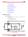
Page 184: Rx Analog Front End
184 www.Xilinx.Com virtex-6 fpga gtx transceivers user guide ug366 (v2.5) january 17, 2011 chapter 4: receiver 6. Rx margin analysis, page 210 7. Rx polarity control, page 213 8. Rx oversampling, page 214 9. Rx pattern checker, page 215 10. Rx byte and word alignment, page 217 11. Rx loss-of-sync st...
Page 185: Www.Bdtic.Com/xilinx
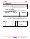
Virtex-6 fpga gtx transceivers user guide www.Xilinx.Com 185 ug366 (v2.5) january 17, 2011 rx analog front end note: mgtavtt_* refers to mgtavtt_s of the south package power plane and mgtavtt_n of the north package power plane, as outlined in figure 5-4, page 277 . Ports and attributes table 4-1 def...
Page 186: Www.Bdtic.Com/xilinx
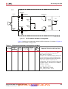
186 www.Xilinx.Com virtex-6 fpga gtx transceivers user guide ug366 (v2.5) january 17, 2011 chapter 4: receiver use modes – rx termination table 4-3 lists the possible settings for rcv_term_gnd and rcv_term_vttrx. Note: mgtavtt_* refers to mgtavtt_s of the south package power plane and mgtavtt_n of t...
Page 187: Www.Bdtic.Com/xilinx
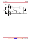
Virtex-6 fpga gtx transceivers user guide www.Xilinx.Com 187 ug366 (v2.5) january 17, 2011 rx analog front end table 4-5 outlines the recommended settings for rx termination in use mode 2. Figure 4-4 shows the use mode 2 configuration. X-ref target - figure 4-3 figure 4-3: rx termination use mode 1 ...
Page 188: Www.Bdtic.Com/xilinx
188 www.Xilinx.Com virtex-6 fpga gtx transceivers user guide ug366 (v2.5) january 17, 2011 chapter 4: receiver x-ref target - figure 4-4 figure 4-4: rx termination use mode 2 configuration ug 3 66_c4_04_120909 ~100 nf nomin a l 50 Ω nomin a l 50 Ω fpga board mgtavtt_ * mgtavtt_ * ~100 nf nomin a l 7...
Page 189: Www.Bdtic.Com/xilinx
Virtex-6 fpga gtx transceivers user guide www.Xilinx.Com 189 ug366 (v2.5) january 17, 2011 rx analog front end table 4-6 outlines the recommended settings for rx termination in use mode 3. Figure 4-5 shows the use mode 3 configuration. Table 4-6: rx termination use mode 3 configuration and notes use...
Page 190: Www.Bdtic.Com/xilinx
190 www.Xilinx.Com virtex-6 fpga gtx transceivers user guide ug366 (v2.5) january 17, 2011 chapter 4: receiver table 4-7 outlines the recommended settings for rx termination in use mode 4. Figure 4-6 shows the use mode 4 configuration. Table 4-7: rx termination use mode 4 configuration and notes use...
Page 191: Www.Bdtic.Com/xilinx
Virtex-6 fpga gtx transceivers user guide www.Xilinx.Com 191 ug366 (v2.5) january 17, 2011 rx analog front end table 4-8 outlines the recommended settings for rx termination in use mode 5. Figure 4-7 shows the use mode 5 configuration. Use mode – resistor calibration for more information on the on-c...
Page 192: Rx Out-of-Band Signaling
192 www.Xilinx.Com virtex-6 fpga gtx transceivers user guide ug366 (v2.5) january 17, 2011 chapter 4: receiver rx out-of-band signaling functional description the gtx receiver provides support for decoding the out-of-band (oob) sequences described in the serial ata (sata) and serial attach scsi (sas...
Page 193: Www.Bdtic.Com/xilinx
Virtex-6 fpga gtx transceivers user guide www.Xilinx.Com 193 ug366 (v2.5) january 17, 2011 rx out-of-band signaling table 4-10 defines the rx oob attributes. Rxstatus[2:0] out rxusrclk2 rxstatus[2:0] are used only for pcie mode, as defined by the pipe specification. Rxvalid out rxusrclk2 indicates s...
Page 194: Rx Equalizer
194 www.Xilinx.Com virtex-6 fpga gtx transceivers user guide ug366 (v2.5) january 17, 2011 chapter 4: receiver rx equalizer functional description the rx has a continuous time rx equalization circuit and a decision feedback equalization circuit to compensate for high-frequency losses in the channel....
Page 195: Www.Bdtic.Com/xilinx
Virtex-6 fpga gtx transceivers user guide www.Xilinx.Com 195 ug366 (v2.5) january 17, 2011 rx equalizer the decision feedback equalizer enhances the internal eye by reducing the post-cursor tail of the transmitted bit. It is a 4-tap architecture. X-ref target - figure 4-10 figure 4-10: relative gain...
Page 196: Www.Bdtic.Com/xilinx
196 www.Xilinx.Com virtex-6 fpga gtx transceivers user guide ug366 (v2.5) january 17, 2011 chapter 4: receiver the dfe allows better compensation of transmission channel losses by providing a closer adjustment of filter parameters than when using a linear equalizer. However, a dfe cannot remove the ...
Page 197: Www.Bdtic.Com/xilinx
Virtex-6 fpga gtx transceivers user guide www.Xilinx.Com 197 ug366 (v2.5) january 17, 2011 rx equalizer ports and attributes table 4-11 defines the rx equalizer ports. Table 4-11: rx equalizer ports port dir clock domain description dfeclkdlyadj[5:0] in rxusrclk2 dfe clock delay adjust override for ...
Page 198: Www.Bdtic.Com/xilinx
198 www.Xilinx.Com virtex-6 fpga gtx transceivers user guide ug366 (v2.5) january 17, 2011 chapter 4: receiver table 4-12 defines the rx equalization attributes. Dfetap3monitor[3:0] out rxusrclk2 dfe tap 3 weight value monitor for each transceiver (3-bit resolution plus 1-bit sign). For example, –2 ...
Page 199: Www.Bdtic.Com/xilinx
Virtex-6 fpga gtx transceivers user guide www.Xilinx.Com 199 ug366 (v2.5) january 17, 2011 rx equalizer use mode – continuous time rx linear e q ualizer only modes with greater gain at high frequencies are intended for lossy (usually longer) channels. Following is a simple way to determine how to us...
Page 200: Www.Bdtic.Com/xilinx
200 www.Xilinx.Com virtex-6 fpga gtx transceivers user guide ug366 (v2.5) january 17, 2011 chapter 4: receiver table 4-14 provides dfetap1 and rxeqmix settings for 4.25 gb/s operation for chip-to-chip applications. Table 4-15 provides dfetap1 and rxeqmix settings for 5 gb/s operation for chip-to-chi...
Page 201: Www.Bdtic.Com/xilinx
Virtex-6 fpga gtx transceivers user guide www.Xilinx.Com 201 ug366 (v2.5) january 17, 2011 rx equalizer table 4-16 provides dfetap1 and rxeqmix settings for 6.25 gb/s operation for chip-to-chip applications. Example – rx linear e q ualizer and dfe settings for backplane applications table 4-17 provi...
Page 202: Www.Bdtic.Com/xilinx
202 www.Xilinx.Com virtex-6 fpga gtx transceivers user guide ug366 (v2.5) january 17, 2011 chapter 4: receiver table 4-18 provides dfetap1 and rxeqmix settings for 4.25 gb/s operation for backplane applications. Table 4-19 provides dfetap1 and rxeqmix settings for 5 gb/s operation for backplane appl...
Page 203: Www.Bdtic.Com/xilinx
Virtex-6 fpga gtx transceivers user guide www.Xilinx.Com 203 ug366 (v2.5) january 17, 2011 rx equalizer table 4-20 provides dfetap1 and rxeqmix settings for 6.25 gb/s operation for backplane applications. Use mode – auto-to-fix this is an advance feature. Use mode – auto this is an advance feature. ...
Page 204: Rx Cdr
204 www.Xilinx.Com virtex-6 fpga gtx transceivers user guide ug366 (v2.5) january 17, 2011 chapter 4: receiver rx cdr functional description the rx clock data recovery (cdr) circuit in each gtx transceiver extracts the recovered clock and data from an incoming data stream. Figure 4-13 illustrates th...
Page 205: Www.Bdtic.Com/xilinx
Virtex-6 fpga gtx transceivers user guide www.Xilinx.Com 205 ug366 (v2.5) january 17, 2011 rx cdr the rx pll provides a base clock to the phase interpolator. The phase interpolator in turn produces fine, evenly spaced sampling phases to allow the cdr state machine to have fine phase control. The cdr...
Page 206: Www.Bdtic.Com/xilinx
206 www.Xilinx.Com virtex-6 fpga gtx transceivers user guide ug366 (v2.5) january 17, 2011 chapter 4: receiver rx_eye_scanmode 2-bit binary this attribute should be set to 00 for normal operation. Refer to rx margin analysis, page 210 for detailed information. Rxpll_divsel_out integer this divider d...
Page 207: Www.Bdtic.Com/xilinx
Virtex-6 fpga gtx transceivers user guide www.Xilinx.Com 207 ug366 (v2.5) january 17, 2011 rx fabric clock output control rx fabric clock output control functional description the rx clock divider control block has two main components: serial clock divider control and parallel clock divider and sele...
Page 208: Www.Bdtic.Com/xilinx
208 www.Xilinx.Com virtex-6 fpga gtx transceivers user guide ug366 (v2.5) january 17, 2011 chapter 4: receiver serial clock divider each receiver pma module has a d divider that divides down the clock from the pll for lower line rate support. This divider can be set statically for applications with ...
Page 209: Www.Bdtic.Com/xilinx
Virtex-6 fpga gtx transceivers user guide www.Xilinx.Com 209 ug366 (v2.5) january 17, 2011 rx fabric clock output control ports and attributes table 4-24 defines the rx clock divider control block ports. Table 4-25 defines the rx clock divider control block attributes. Table 4-24: rx clock divider c...
Page 210: Rx Margin Analysis
210 www.Xilinx.Com virtex-6 fpga gtx transceivers user guide ug366 (v2.5) january 17, 2011 chapter 4: receiver rx margin analysis functional description as line rates and channel attenuation increase, the receiver equalizers are often enabled to overcome channel attenuation. This posts a challenge t...
Page 211: Www.Bdtic.Com/xilinx
Virtex-6 fpga gtx transceivers user guide www.Xilinx.Com 211 ug366 (v2.5) january 17, 2011 rx margin analysis as illustrated in figure 4-17 , when the data sampling phase approaches the edge transition region, user logic observes a corresponding increased in bit error rate on the received user data....
Page 212: Www.Bdtic.Com/xilinx
212 www.Xilinx.Com virtex-6 fpga gtx transceivers user guide ug366 (v2.5) january 17, 2011 chapter 4: receiver eye outline scan mode this method provides diagnostic information related to the deterministic eye shape, particularly the vertical eye opening. Setting rx_eye_scanmode to 01 suspends the d...
Page 213: Rx Polarity Control
Virtex-6 fpga gtx transceivers user guide www.Xilinx.Com 213 ug366 (v2.5) january 17, 2011 rx polarity control table 4-27 defines the rx margin analysis attributes. Rx polarity control functional description the gtx rx can invert incoming data using the rx polarity control function. This function is...
Page 214: Rx Oversampling
214 www.Xilinx.Com virtex-6 fpga gtx transceivers user guide ug366 (v2.5) january 17, 2011 chapter 4: receiver rx oversampling feature description each gtx transceiver includes built-in 5x oversampling to enable serial rates from 1/10 th of the lower border of the frequency range of the rx pma pll u...
Page 215: Rx Pattern Checker
Virtex-6 fpga gtx transceivers user guide www.Xilinx.Com 215 ug366 (v2.5) january 17, 2011 rx pattern checker ports and attributes table 4-29 defines the rx oversampling ports. Table 4-30 defines the rx oversampling attributes. Rx pattern checker functional description the gtx receiver includes a bu...
Page 216: Www.Bdtic.Com/xilinx
216 www.Xilinx.Com virtex-6 fpga gtx transceivers user guide ug366 (v2.5) january 17, 2011 chapter 4: receiver ports and attributes table 4-31 defines the pattern checker ports. Table 4-32 defines the pattern checker attributes. Table 4-33 defines the rx pattern checker registers. Use models to use ...
Page 217: Rx Byte and Word Alignment
Virtex-6 fpga gtx transceivers user guide www.Xilinx.Com 217 ug366 (v2.5) january 17, 2011 rx byte and word alignment data. If the incoming data is inverted by transmitter or reversed rxp/rxn, the received data should also inverted by controlling rxpolarity. Otherwise, the prbs checker will not lock...
Page 218: Www.Bdtic.Com/xilinx
218 www.Xilinx.Com virtex-6 fpga gtx transceivers user guide ug366 (v2.5) january 17, 2011 chapter 4: receiver the gtx transceiver includes an alignment block that can be programmed to align specific commas to various byte boundaries, or to manually align data using attribute settings (see figure 4-...
Page 219: Www.Bdtic.Com/xilinx
Virtex-6 fpga gtx transceivers user guide www.Xilinx.Com 219 ug366 (v2.5) january 17, 2011 rx byte and word alignment on rx_data_width. Either a 16-bit or a 20-bit comma alignment mode is possible. Figure 4-24 shows how the commas are combined when comma_double is true. Figure 4-25 shows how comma_1...
Page 220: Www.Bdtic.Com/xilinx
220 www.Xilinx.Com virtex-6 fpga gtx transceivers user guide ug366 (v2.5) january 17, 2011 chapter 4: receiver alignment boundaries the allowed boundaries for alignment are defined by align_comma_word. The spacing of the possible boundaries is determined by rx_data_width, and the number of boundary ...
Page 221: Www.Bdtic.Com/xilinx
Virtex-6 fpga gtx transceivers user guide www.Xilinx.Com 221 ug366 (v2.5) january 17, 2011 rx byte and word alignment x-ref target - figure 4-27 figure 4-27: manual data alignment using rxslide for rx_data_width = 20 bits rxusrclk2 rxslide rxdata txdata slide results on rxdata after several cycles o...
Page 222: Www.Bdtic.Com/xilinx
222 www.Xilinx.Com virtex-6 fpga gtx transceivers user guide ug366 (v2.5) january 17, 2011 chapter 4: receiver ports and attributes table 4-34 defines the rx comma alignment and detection ports. Table 4-34: rx comma alignment and detection ports port dir clock domain description rxbyteisaligned out ...
Page 223: Www.Bdtic.Com/xilinx
Virtex-6 fpga gtx transceivers user guide www.Xilinx.Com 223 ug366 (v2.5) january 17, 2011 rx byte and word alignment table 4-35 defines the rx comma alignment attributes. Rxslide in rxusrclk2 rxslide implements a comma alignment bump control. When rxslide is asserted, the byte alignment is adjusted...
Page 224: Www.Bdtic.Com/xilinx
224 www.Xilinx.Com virtex-6 fpga gtx transceivers user guide ug366 (v2.5) january 17, 2011 chapter 4: receiver comma_double boolean specifies whether a comma match consists of either a comma plus or a comma minus alone, or whether both are required in the sequence. False: the plus comma (pcomma) and...
Page 225: Www.Bdtic.Com/xilinx
Virtex-6 fpga gtx transceivers user guide www.Xilinx.Com 225 ug366 (v2.5) january 17, 2011 rx byte and word alignment rx_slide_mode string defines the rxslide mode: off: this is the default setting. The rxslide feature is not used. Pcs: the pcs is used to perform the bit slipping function. Rxslide i...
Page 226: Www.Bdtic.Com/xilinx
226 www.Xilinx.Com virtex-6 fpga gtx transceivers user guide ug366 (v2.5) january 17, 2011 chapter 4: receiver rx loss-of-sync state machine functional description several 8b/10b protocols make use of a standard loss-of-sync (los) state machine to detect when the channel is malfunctioning. Each gtx ...
Page 227: Www.Bdtic.Com/xilinx
Virtex-6 fpga gtx transceivers user guide www.Xilinx.Com 227 ug366 (v2.5) january 17, 2011 rx loss-of-sync state machine loss_of_sync state. The rx_los_threshold entry in table 4-37 shows the valid settings for this attribute. The los state machine allows the error count in the sync_acquired state t...
Page 228: Rx 8B/10B Decoder
228 www.Xilinx.Com virtex-6 fpga gtx transceivers user guide ug366 (v2.5) january 17, 2011 chapter 4: receiver rx 8b/10b decoder functional description many protocols require receivers to decode 8b/10b data. 8b/10b is an industry standard encoding scheme that trades two bits of overhead per byte for...
Page 229: Www.Bdtic.Com/xilinx
Virtex-6 fpga gtx transceivers user guide www.Xilinx.Com 229 ug366 (v2.5) january 17, 2011 rx 8b/10b decoder rx running disparity 8b/10b includes special characters (k characters) that are often used for control functions. When rxdata is a k character, the decoder drives rxcharisk high. If dec_pcomm...
Page 230: Www.Bdtic.Com/xilinx
230 www.Xilinx.Com virtex-6 fpga gtx transceivers user guide ug366 (v2.5) january 17, 2011 chapter 4: receiver ports and attributes table 4-38 defines the rx decoder ports. Table 4-38: rx decoder ports port dir clock domain description rxchariscomma[3:0] out rxusrclk2 rxchariscomma indicates that th...
Page 231: Rx Buffer Bypass
Virtex-6 fpga gtx transceivers user guide www.Xilinx.Com 231 ug366 (v2.5) january 17, 2011 rx buffer bypass table 4-39 defines the rx decoder attributes. Rx buffer bypass functional description bypassing the rx buffer is an advanced feature of the virtex-6 fpga gtx transceivers. Rx buffer bypass can...
Page 232: Www.Bdtic.Com/xilinx
232 www.Xilinx.Com virtex-6 fpga gtx transceivers user guide ug366 (v2.5) january 17, 2011 chapter 4: receiver the cdr to be adjusted so that there is no significant phase difference between xclk and rxusrclk. Note: bypassing the rx buffer is an advanced feature. Rx buffer bypass can operate only un...
Page 233: Www.Bdtic.Com/xilinx
Virtex-6 fpga gtx transceivers user guide www.Xilinx.Com 233 ug366 (v2.5) january 17, 2011 rx buffer bypass table 4-40: rx buffer bypass ports port dir clock domain description rxdlyaligndisable in async rx delay aligner enable/disable signal. When driven low, it enables the delay phase aligner. Rxd...
Page 234: Www.Bdtic.Com/xilinx
234 www.Xilinx.Com virtex-6 fpga gtx transceivers user guide ug366 (v2.5) january 17, 2011 chapter 4: receiver table 4-41 defines the rx buffer bypass attributes. Table 4-41: rx buffer bypass attributes attribute type description power_save 10-bit binary power_save[4]: mux select for the txoutclk ou...
Page 235: Www.Bdtic.Com/xilinx
Virtex-6 fpga gtx transceivers user guide www.Xilinx.Com 235 ug366 (v2.5) january 17, 2011 rx buffer bypass using the rx phase alignment circuit to bypass the buffer bypassing the rx buffer is an advanced feature. Rx buffer bypass can operate only under certain system-level conditions. To use the rx...
Page 236: Www.Bdtic.Com/xilinx
236 www.Xilinx.Com virtex-6 fpga gtx transceivers user guide ug366 (v2.5) january 17, 2011 chapter 4: receiver figure 4-32 shows the rx phase alignment procedure. Notes for figure 4-32 . 1. Assert this signal when rxusrclk/rxusrclk2 clocks are stabilized. 2. Repeat the rxpmasetphase procedure if bad...
Page 237: Www.Bdtic.Com/xilinx
Virtex-6 fpga gtx transceivers user guide www.Xilinx.Com 237 ug366 (v2.5) january 17, 2011 rx buffer bypass x-ref target - figure 4-33 figure 4-33: steps required for successful rx phase alignment a ss ert rxpma s etpha s e for 3 2 rxu s rclk2 cycle s to ph as e align w a it for mmcm lock. Rxn/rxp s...
Page 238: Rx Elastic Buffer
238 www.Xilinx.Com virtex-6 fpga gtx transceivers user guide ug366 (v2.5) january 17, 2011 chapter 4: receiver rx elastic buffer functional description the gtx rx datapath has two internal parallel clock domains used in the pcs: the pma parallel clock domain (xclk) and the rxusrclk domain. To receiv...
Page 239: Www.Bdtic.Com/xilinx
Virtex-6 fpga gtx transceivers user guide www.Xilinx.Com 239 ug366 (v2.5) january 17, 2011 rx elastic buffer ports and attributes table 4-43 defines the rx elastic buffer ports. Table 4-44 defines the rx elastic buffer attributes. Table 4-43: rx elastic buffer ports port dir clock domain description...
Page 240: Rx Clock Correction
240 www.Xilinx.Com virtex-6 fpga gtx transceivers user guide ug366 (v2.5) january 17, 2011 chapter 4: receiver using the rx elastic buffer for channel bonding or clock correction the rx elastic buffer is also used for clock correction (see rx clock correction ) and channel bonding (see rx channel bo...
Page 241: Www.Bdtic.Com/xilinx
Virtex-6 fpga gtx transceivers user guide www.Xilinx.Com 241 ug366 (v2.5) january 17, 2011 rx clock correction clock correction should be used whenever there is a frequency difference between xclk and rxusrclk. It can be avoided by using the same frequency source for tx and rx, or by using the recov...
Page 242: Www.Bdtic.Com/xilinx
242 www.Xilinx.Com virtex-6 fpga gtx transceivers user guide ug366 (v2.5) january 17, 2011 chapter 4: receiver table 4-47 defines the rx clock correction attributes. Rxclkcorcnt[2:0] out rxusrclk2 reports the clock correction status of the rx elastic buffer: 000 : no clock correction 001 : 1 sequenc...
Page 243: Www.Bdtic.Com/xilinx
Virtex-6 fpga gtx transceivers user guide www.Xilinx.Com 243 ug366 (v2.5) january 17, 2011 rx clock correction clk_cor_min_lat integer specifies the minimum rx elastic buffer latency. If the rx elastic buffer drops below clk_cor_min_lat, the clock correction circuit replicates incoming clock correct...
Page 244: Www.Bdtic.Com/xilinx
244 www.Xilinx.Com virtex-6 fpga gtx transceivers user guide ug366 (v2.5) january 17, 2011 chapter 4: receiver clk_cor_seq_2_1 10-bit binary the clk_cor_seq_2 attributes are used in conjunction with clk_cor_seq_2_enable to define the second clock correction sequence. This second sequence is used as ...
Page 245: Www.Bdtic.Com/xilinx
Virtex-6 fpga gtx transceivers user guide www.Xilinx.Com 245 ug366 (v2.5) january 17, 2011 rx clock correction using rx clock correction the user must follow the steps described in this section to use the receiver clock correction. Enabling clock correction each gtx transceiver includes a clock corr...
Page 246: Www.Bdtic.Com/xilinx
246 www.Xilinx.Com virtex-6 fpga gtx transceivers user guide ug366 (v2.5) january 17, 2011 chapter 4: receiver some protocols use clock correction sequences with don’t care subsequences. The clock correction circuit can be programmed to recognize these sequences using clk_cor_seq_1_enable and clk_co...
Page 247: Rx Channel Bonding
Virtex-6 fpga gtx transceivers user guide www.Xilinx.Com 247 ug366 (v2.5) january 17, 2011 rx channel bonding rx channel bonding functional description the rx elastic buffer can also be used for channel bonding. Channel bonding cancels out the skew between gtx transceiver lanes by using the rx elast...
Page 248: Www.Bdtic.Com/xilinx
248 www.Xilinx.Com virtex-6 fpga gtx transceivers user guide ug366 (v2.5) january 17, 2011 chapter 4: receiver table 4-49 defines the rx channel bonding attributes. Rxchanrealign out rxusrclk2 this signal from the rx elastic buffer is held high for at least one cycle when the receiver has changed th...
Page 249: Www.Bdtic.Com/xilinx
Virtex-6 fpga gtx transceivers user guide www.Xilinx.Com 249 ug366 (v2.5) january 17, 2011 rx channel bonding table 4-49: rx channel bonding attributes attribute type description chan_bond_1_max_skew integer these attributes control the number of usrclk cycles that the master waits before ordering t...
Page 250: Www.Bdtic.Com/xilinx
250 www.Xilinx.Com virtex-6 fpga gtx transceivers user guide ug366 (v2.5) january 17, 2011 chapter 4: receiver using rx channel bonding the user must follow the steps described below in order to use the receiver channel bonding. Enabling channel bonding each gtx transceiver includes a circuit that p...
Page 251: Www.Bdtic.Com/xilinx
Virtex-6 fpga gtx transceivers user guide www.Xilinx.Com 251 ug366 (v2.5) january 17, 2011 rx channel bonding connecting channel bonding ports the channel bonding operation requires connecting the master gtx rxchbondo port to the rxchbondi port of all slaves in the group. A direct connection is requ...
Page 252: Www.Bdtic.Com/xilinx
252 www.Xilinx.Com virtex-6 fpga gtx transceivers user guide ug366 (v2.5) january 17, 2011 chapter 4: receiver to set up a daisy chain, first connect the gtx transceivers using rxchbondo and rxchbondi to create a path from the rxchbondi port of each slave to the rxchbondo port of the master. Use the...
Page 253: Www.Bdtic.Com/xilinx
Virtex-6 fpga gtx transceivers user guide www.Xilinx.Com 253 ug366 (v2.5) january 17, 2011 rx channel bonding as long as timing constraints are met, the following items apply: • there is no limit to the number of gtx transceivers that can be on a particular rxchanbondlevel[2:0]. • gtx transceivers c...
Page 254: Www.Bdtic.Com/xilinx
254 www.Xilinx.Com virtex-6 fpga gtx transceivers user guide ug366 (v2.5) january 17, 2011 chapter 4: receiver setting channel bonding se q uences the channel bonding sequence is programmed in the same way as the clock correction sequence. Chan_bond_seq_len sets the length of the sequence, and chan_...
Page 255: Www.Bdtic.Com/xilinx
Virtex-6 fpga gtx transceivers user guide www.Xilinx.Com 255 ug366 (v2.5) january 17, 2011 rx channel bonding chan_bond_1_max_skew and chan_bond_2_max_skew are used to set the maximum skew allowed for channel bonding sequences 1 and 2, respectively. The maximum skew range is 1 to 14. This range must...
Page 256: Rx Gearbox
256 www.Xilinx.Com virtex-6 fpga gtx transceivers user guide ug366 (v2.5) january 17, 2011 chapter 4: receiver rx gearbox functional description the rx gearbox uses output pins rxdata[31:0] and rxheader[2:0] for receiving data. Similar to tx gearbox, page 146 , the rx gearbox operates with the pma u...
Page 257: Www.Bdtic.Com/xilinx
Virtex-6 fpga gtx transceivers user guide www.Xilinx.Com 257 ug366 (v2.5) january 17, 2011 rx gearbox enabling the rx gearbox to enable the rx gearbox for the gtx transceiver, the rxgearbox_use attribute is set to true. Bit 2 of the gearbox_endec attribute must be set to 0 to enable the gearbox deco...
Page 258: Www.Bdtic.Com/xilinx
258 www.Xilinx.Com virtex-6 fpga gtx transceivers user guide ug366 (v2.5) january 17, 2011 chapter 4: receiver rx gearbox block synchronization the 64b/66b and 64b/67b protocols depend on block synchronization to determine their block boundaries. Block synchronization is required because all incomin...
Page 259: Www.Bdtic.Com/xilinx
Virtex-6 fpga gtx transceivers user guide www.Xilinx.Com 259 ug366 (v2.5) january 17, 2011 rx gearbox the state machine works by keeping track of valid and invalid synchronization headers. Upon reset, block lock is deasserted, and the state is lock_init. The next state is reset_cnt where all counter...
Page 260: Www.Bdtic.Com/xilinx
260 www.Xilinx.Com virtex-6 fpga gtx transceivers user guide ug366 (v2.5) january 17, 2011 chapter 4: receiver for the block synchronization state machine shown in figure 4-47 , sh_cnt_max and sh_invalid_cnt_max are both constants that are set to 64 and 16, respectively. From the valid_sh state, if ...
Page 261: Rx Initialization
Virtex-6 fpga gtx transceivers user guide www.Xilinx.Com 261 ug366 (v2.5) january 17, 2011 rx initialization rx initialization functional description the gtx rx must be reset before it can be used. There are three ways to reset the gtx rx: 1. Power up and configure the fpga. Power-up reset is covere...
Page 262: Www.Bdtic.Com/xilinx
262 www.Xilinx.Com virtex-6 fpga gtx transceivers user guide ug366 (v2.5) january 17, 2011 chapter 4: receiver table 4-53 defines the rx initialization attributes. Rxbufreset in async pcs rx elastic buffer reset. This active-high signal resets the rx elastic buffer logic; it resets the pointers in t...
Page 263: Www.Bdtic.Com/xilinx
Virtex-6 fpga gtx transceivers user guide www.Xilinx.Com 263 ug366 (v2.5) january 17, 2011 rx initialization gtx rx reset in response to completion of configuration figure 4-50 shows the gtx rx reset following the completion of configuration of a powered-up gtx transceiver. The same sequence is acti...
Page 264: Www.Bdtic.Com/xilinx
264 www.Xilinx.Com virtex-6 fpga gtx transceivers user guide ug366 (v2.5) january 17, 2011 chapter 4: receiver link idle reset support the link idle reset circuitry is built into the gtx receiver. The rx elastic buffer reset sequence during an electrical idle condition is available for additional fu...
Page 265: Www.Bdtic.Com/xilinx
Virtex-6 fpga gtx transceivers user guide www.Xilinx.Com 265 ug366 (v2.5) january 17, 2011 rx initialization table 4-55 lists the recommended resets for various situations. Table 4-54: available receiver resets and the components reset by them component configuration gt x r xr es et rxpllpo w erdo w...
Page 266: Www.Bdtic.Com/xilinx
266 www.Xilinx.Com virtex-6 fpga gtx transceivers user guide ug366 (v2.5) january 17, 2011 chapter 4: receiver after power-up and configuration the entire gtx rx is reset automatically after the configuration-provided rxpllpowerdown is low. The supplies for the calibration resistor and calibration r...
Page 267: Www.Bdtic.Com/xilinx
Virtex-6 fpga gtx transceivers user guide www.Xilinx.Com 267 ug366 (v2.5) january 17, 2011 rx initialization if the reference clock(s) or gtx transceiver(s) are powered up after configuration, gtxrxreset must be asserted to allow the rx pll(s) to lock. After changing the reference clock to rx pll wh...
Page 268: Www.Bdtic.Com/xilinx
268 www.Xilinx.Com virtex-6 fpga gtx transceivers user guide ug366 (v2.5) january 17, 2011 chapter 4: receiver after connecting rxn/rxp when the rx data to the gtx transceiver comes from a connector that can be plugged in and unplugged, the rx cdr must be reset when the data source is plugged in to ...
Page 269: Fpga Rx Interface
Virtex-6 fpga gtx transceivers user guide www.Xilinx.Com 269 ug366 (v2.5) january 17, 2011 fpga rx interface after comma realignment when set to true, rx_en_realign_reset_buf enables automatic reset of the rx elastic buffer during comma realignment. Fpga rx interface functional description the fpga ...
Page 270: Www.Bdtic.Com/xilinx
270 www.Xilinx.Com virtex-6 fpga gtx transceivers user guide ug366 (v2.5) january 17, 2011 chapter 4: receiver 16 to 20 bits, or 32 to 40 bits. Table 4-57 shows the data received when the 8b/10b decoder is disabled. Rxusrclk and rxusrclk2 generation the fpga rx interface includes two parallel clocks...
Page 271: Www.Bdtic.Com/xilinx
Virtex-6 fpga gtx transceivers user guide www.Xilinx.Com 271 ug366 (v2.5) january 17, 2011 fpga rx interface the following rules about the relationships between clocks must be observed for rxusrclk and rxusrclk2: • rxusrclk and rxusrclk2 must be positive-edge aligned, with as little skew as possible...
Page 272: Www.Bdtic.Com/xilinx
272 www.Xilinx.Com virtex-6 fpga gtx transceivers user guide ug366 (v2.5) january 17, 2011 chapter 4: receiver table 4-61 defines the fpga rx attributes. Rxusrclk in clock this port provides a clock for the internal rx pcs datapath. In some use cases, this clock is internally generated. See table 4-...
Page 273: Board Design Guidelines
Virtex-6 fpga gtx transceivers user guide www.Xilinx.Com 273 ug366 (v2.5) january 17, 2011 chapter 5 board design guidelines overview this chapter discusses topics related to implementing a design that uses the virtex®-6 fpga gtx transceiver on a printed circuit board (pcb). The gtx transceivers are...
Page 274: Www.Bdtic.Com/xilinx
274 www.Xilinx.Com virtex-6 fpga gtx transceivers user guide ug366 (v2.5) january 17, 2011 chapter 5: board design guidelines figure 5-1 shows the connections of the power supply pins for the gtx transceiver. The listed voltages are nominal values. Refer to the virtex-6 fpga data sheet for values an...
Page 275: Www.Bdtic.Com/xilinx
Virtex-6 fpga gtx transceivers user guide www.Xilinx.Com 275 ug366 (v2.5) january 17, 2011 pin description and design guidelines the mgtavttrcal pin should be connected to the mgtavtt supply and to a pin on the 100 precision external resistor. The other pin of the resistor is connected to the mgtrre...
Page 276: Www.Bdtic.Com/xilinx
276 www.Xilinx.Com virtex-6 fpga gtx transceivers user guide ug366 (v2.5) january 17, 2011 chapter 5: board design guidelines managing unused gtx transceivers in many applications, only a portion of the gtx transceivers are required. There are considerations for managing the unused gtx transceivers ...
Page 277: Www.Bdtic.Com/xilinx
Virtex-6 fpga gtx transceivers user guide www.Xilinx.Com 277 ug366 (v2.5) january 17, 2011 pin description and design guidelines figure 5-4 shows the orientation in the device of the quad power banks within a device. The type of grouping for the quads in a column depends on the device package. The f...
Page 278: Www.Bdtic.Com/xilinx
278 www.Xilinx.Com virtex-6 fpga gtx transceivers user guide ug366 (v2.5) january 17, 2011 chapter 5: board design guidelines partially unused quad column if only a portion of the quads is used, there are two possible scenarios that affect how the quad pins can be connected. For the first scenario, ...
Page 279: Www.Bdtic.Com/xilinx
Virtex-6 fpga gtx transceivers user guide www.Xilinx.Com 279 ug366 (v2.5) january 17, 2011 pin description and design guidelines partially used quad there are four gtx transceivers in a quad. For a partially used quad where one or more transceivers (but not all) are unused, the analog power supplies...
Page 280: Reference Clock
280 www.Xilinx.Com virtex-6 fpga gtx transceivers user guide ug366 (v2.5) january 17, 2011 chapter 5: board design guidelines depending on availability in the package, these quads have equal priority. North/south package power plane prioritization • priority 1: mgt115 this quad should be used if any...
Page 281: Www.Bdtic.Com/xilinx
Virtex-6 fpga gtx transceivers user guide www.Xilinx.Com 281 ug366 (v2.5) january 17, 2011 reference clock figure 5-6 illustrates the differential clock input voltage swing, peak-to-peak, which is defined as mgtrefclkp – mgtrefclkn. Figure 5-7 shows the rise and fall time convention of the reference...
Page 282: Www.Bdtic.Com/xilinx
282 www.Xilinx.Com virtex-6 fpga gtx transceivers user guide ug366 (v2.5) january 17, 2011 chapter 5: board design guidelines reference clock checklist the following criteria must be met when choosing an oscillator for a design with gtx transceivers: • provide ac coupling between the oscillator outp...
Page 283: Power Supply And Filtering
Virtex-6 fpga gtx transceivers user guide www.Xilinx.Com 283 ug366 (v2.5) january 17, 2011 power supply and filtering ac coupled reference clock ac coupling of the oscillator reference clock output to the quad reference clock inputs serves multiple purposes: • dc current is blocked between the oscil...
Page 284: Www.Bdtic.Com/xilinx
284 www.Xilinx.Com virtex-6 fpga gtx transceivers user guide ug366 (v2.5) january 17, 2011 chapter 5: board design guidelines power supply pins, page 276 for a discussion of the internal power planes in the virtex-6 fpga packages. Noise on the gtx analog power supplies can cause degradation in the p...
Page 285: Www.Bdtic.Com/xilinx
Virtex-6 fpga gtx transceivers user guide www.Xilinx.Com 285 ug366 (v2.5) january 17, 2011 power supply and filtering there are potentially two major disadvantages to linear regulators: minimum dropout voltage and limited efficiency. Linear regulators require an input voltage that is higher than the...
Page 286: Www.Bdtic.Com/xilinx
286 www.Xilinx.Com virtex-6 fpga gtx transceivers user guide ug366 (v2.5) january 17, 2011 chapter 5: board design guidelines power supply distribution network staged decoupling die there is decoupling capacitance on the die to filter the highest frequency noise components on the power supplies. The...
Page 287: Www.Bdtic.Com/xilinx
Virtex-6 fpga gtx transceivers user guide www.Xilinx.Com 287 ug366 (v2.5) january 17, 2011 power supply and filtering this subsection discusses some issues regarding the implementation of these design issues on the pcb. Board stackup for virtex-6 fpga gtx transceivers, the board stackup layers can b...
Page 288: Www.Bdtic.Com/xilinx
288 www.Xilinx.Com virtex-6 fpga gtx transceivers user guide ug366 (v2.5) january 17, 2011 chapter 5: board design guidelines layers above and below the power planes. Because of their low impedance, power planes are often prime candidates for providing return current paths for signals routed above o...
Page 289: Www.Bdtic.Com/xilinx
Virtex-6 fpga gtx transceivers user guide www.Xilinx.Com 289 ug366 (v2.5) january 17, 2011 power supply and filtering signal bga breakout the receiver, transmitter, and reference clock signals must be routed from the bga pin field to destinations on the pcb. The signal routing layers provide the rou...
Page 290: Www.Bdtic.Com/xilinx
290 www.Xilinx.Com virtex-6 fpga gtx transceivers user guide ug366 (v2.5) january 17, 2011 chapter 5: board design guidelines for signals that are on the inner rows of pins, it is necessary to route from the bga pin pad on top of the board to a via. The signal pair is routed from each via by stripli...
Page 291: Hot Swapping Devices
Virtex-6 fpga gtx transceivers user guide www.Xilinx.Com 291 ug366 (v2.5) january 17, 2011 hot swapping devices crosstalk crosstalk is a major contributor to degradation in the performance of a gtx transceiver. The mechanisms for crosstalk are aggressor signals coupling into signal traces and/or cou...
Page 292: Www.Bdtic.Com/xilinx
292 www.Xilinx.Com virtex-6 fpga gtx transceivers user guide ug366 (v2.5) january 17, 2011 chapter 5: board design guidelines • eliminate routing of gtx transceiver signals and selectio interface signals on adjacent layers. Be aware of the potential of broadside coupling if these signals are routed ...
Page 293: 8B/10B Valid Characters
Virtex-6 fpga gtx transceivers user guide www.Xilinx.Com 293 ug366 (v2.5) january 17, 2011 appendix a 8b/10b valid characters 8b/10b encoding includes a set of data characters and k characters. Eight-bit values are coded into 10-bit values, keeping the serial line dc balanced. K characters are speci...
Page 294: Www.Bdtic.Com/xilinx
294 www.Xilinx.Com virtex-6 fpga gtx transceivers user guide ug366 (v2.5) january 17, 2011 appendix a: 8b/10b valid characters d21.0 000 10101 101010 1011 101010 0100 d22.0 000 10110 011010 1011 011010 0100 d23.0 000 10111 111010 0100 000101 1011 d24.0 000 11000 110011 0100 001100 1011 d25.0 000 110...
Page 295: Www.Bdtic.Com/xilinx
Virtex-6 fpga gtx transceivers user guide www.Xilinx.Com 295 ug366 (v2.5) january 17, 2011 d21.1 001 10101 101010 1001 101010 1001 d22.1 001 10110 011010 1001 011010 1001 d23.1 001 10111 111010 1001 000101 1001 d24.1 001 11000 110011 1001 001100 1001 d25.1 001 11001 100110 1001 100110 1001 d26.1 001...
Page 296: Www.Bdtic.Com/xilinx
296 www.Xilinx.Com virtex-6 fpga gtx transceivers user guide ug366 (v2.5) january 17, 2011 appendix a: 8b/10b valid characters d21.2 010 10101 101010 0101 101010 0101 d22.2 010 10110 011010 0101 011010 0101 d23.2 010 10111 111010 0101 000101 0101 d24.2 010 11000 110011 0101 001100 0101 d25.2 010 110...
Page 297: Www.Bdtic.Com/xilinx
Virtex-6 fpga gtx transceivers user guide www.Xilinx.Com 297 ug366 (v2.5) january 17, 2011 d21.3 011 10101 101010 1100 101010 0011 d22.3 011 10110 011010 1100 011010 0011 d23.3 011 10111 111010 0011 000101 1100 d24.3 011 11000 110011 0011 001100 1100 d25.3 011 11001 100110 1100 100110 0011 d26.3 011...
Page 298: Www.Bdtic.Com/xilinx
298 www.Xilinx.Com virtex-6 fpga gtx transceivers user guide ug366 (v2.5) january 17, 2011 appendix a: 8b/10b valid characters d21.4 100 10101 101010 1101 101010 0010 d22.4 100 10110 011010 1101 011010 0010 d23.4 100 10111 111010 0010 000101 1101 d24.4 100 11000 110011 0010 001100 1101 d25.4 100 110...
Page 299: Www.Bdtic.Com/xilinx
Virtex-6 fpga gtx transceivers user guide www.Xilinx.Com 299 ug366 (v2.5) january 17, 2011 d21.5 101 10101 101010 1010 101010 1010 d22.5 101 10110 011010 1010 011010 1010 d23.5 101 10111 111010 1010 000101 1010 d24.5 101 11000 110011 1010 001100 1010 d25.5 101 11001 100110 1010 100110 1010 d26.5 101...
Page 300: Www.Bdtic.Com/xilinx
300 www.Xilinx.Com virtex-6 fpga gtx transceivers user guide ug366 (v2.5) january 17, 2011 appendix a: 8b/10b valid characters d21.6 110 10101 101010 0110 101010 0110 d22.6 110 10110 011010 0110 011010 0110 d23.6 110 10111 111010 0110 000101 0110 d24.6 110 11000 110011 0110 001100 0110 d25.6 110 110...
Page 301: Www.Bdtic.Com/xilinx
Virtex-6 fpga gtx transceivers user guide www.Xilinx.Com 301 ug366 (v2.5) january 17, 2011 d21.7 111 10101 101010 1110 101010 0001 d22.7 111 10110 011010 1110 011010 0001 d23.7 111 10111 111010 0001 000101 1110 d24.7 111 11000 110011 0001 001100 1110 d25.7 111 11001 100110 1110 100110 0001 d26.7 111...
Page 302: Www.Bdtic.Com/xilinx
302 www.Xilinx.Com virtex-6 fpga gtx transceivers user guide ug366 (v2.5) january 17, 2011 appendix a: 8b/10b valid characters www.Bdtic.Com/xilinx.
Page 303: Drp Address Map of The Gtx
Virtex-6 fpga gtx transceivers user guide www.Xilinx.Com 303 ug366 (v2.5) january 17, 2011 appendix b drp address map of the gtx transceiver table b-1 and table b-2 list the drp map sorted by address. Note: do not modify the reserved bits! Attributes that are not described explicitly are set automat...
Page 304: Www.Bdtic.Com/xilinx
304 www.Xilinx.Com virtex-6 fpga gtx transceivers user guide ug366 (v2.5) january 17, 2011 appendix b: drp address map of the gtx transceiver 6h 15:13 r/w rx_los_invalid_incr 2:0 1 000 2 001 4 010 8 011 16 100 32 101 64 110 128 111 12:10 rx_los_threshold 2:0 4 000 8 001 16 010 32 011 64 100 128 101 ...
Page 305: Www.Bdtic.Com/xilinx
Virtex-6 fpga gtx transceivers user guide www.Xilinx.Com 305 ug366 (v2.5) january 17, 2011 bh 15:12 r/w rx_idle_hi_cnt 3:0 0-15 1 (1) 11 rx_xclk_sel rxrec 0 rxusr 1 10 rx_en_idle_reset_buf false 0 true 1 9:0 chan_bond_seq_2_4 9:0 0-1023 1 (1) ch 15:14 r/w reserved 1:0 13 rx_fifo_addr_mode false 0 tr...
Page 306: Www.Bdtic.Com/xilinx
306 www.Xilinx.Com virtex-6 fpga gtx transceivers user guide ug366 (v2.5) january 17, 2011 appendix b: drp address map of the gtx transceiver 13h 15:12 r/w rx_slide_auto_wait 3:0 0-15 1 (1) 11:10 clk_cor_det_len 1:0 1 00 2 01 reserved 4 11 9:0 clk_cor_seq_2_3 9:0 0-1023 1 (1) 14h 15 r/w dec_valid_co...
Page 307: Www.Bdtic.Com/xilinx
Virtex-6 fpga gtx transceivers user guide www.Xilinx.Com 307 ug366 (v2.5) january 17, 2011 17h 15 r/w gen_rxusrclk false 0 true 1 14:12 rx_data_width 2:0 20 011 8 000 10 001 16 010 32 100 40 101 11 chan_bond_seq_2_cfg 4 0-31 1 (1) 10 bias_cfg 16 9:5 rx_clk25_divider 4:0 6 00101 1 00000 2 00001 3 000...
Page 308: Www.Bdtic.Com/xilinx
308 www.Xilinx.Com virtex-6 fpga gtx transceivers user guide ug366 (v2.5) january 17, 2011 appendix b: drp address map of the gtx transceiver 18h 15:4 r/w reserved 11:0 3 rxgearbox_use false 0 true 1 2:0 gearbox_endec 2:0 0-7 1 (1) 19h 15:0 r/w rxpll_com_cfg 15:0 1ah 15:8 r/w rxpll_cp_cfg 7:0 7:0 rx...
Page 309: Www.Bdtic.Com/xilinx
Virtex-6 fpga gtx transceivers user guide www.Xilinx.Com 309 ug366 (v2.5) january 17, 2011 20h 15 r/w tx_oversample_mode false 0 true 1 14:6 reserved 8:0 5:1 txpll_divsel_ref 4:0 1 10000 2 00000 0 reserved 21h 15 r/w pci_express_mode false 0 true 1 14 reserved 13:0 tx_detect_rx_cfg 13:0 22h 15 pma_c...
Page 310: Www.Bdtic.Com/xilinx
310 www.Xilinx.Com virtex-6 fpga gtx transceivers user guide ug366 (v2.5) january 17, 2011 appendix b: drp address map of the gtx transceiver 23h 15 r/w reserved 14:10 tx_clk25_divider 4:0 6 00101 1 00000 2 00001 3 00010 4 00011 5 00100 7 00110 8 00111 9 01000 10 01001 11 01010 12 01011 13 01100 14 ...
Page 311: Www.Bdtic.Com/xilinx
Virtex-6 fpga gtx transceivers user guide www.Xilinx.Com 311 ug366 (v2.5) january 17, 2011 27h 15 r/w tx_en_rate_reset_buf false 0 true 1 14:12 sata_idle_val 2:0 0-7 1 (1) 11:6 sata_min_init 5:0 1-61 1 (1) 5:0 sata_max_init 5:0 1-61 1 (1) 28h 15 r/w reserved 14:12 sata_burst_val 2:0 0-7 1 (1) 11:6 s...
Page 312: Www.Bdtic.Com/xilinx
312 www.Xilinx.Com virtex-6 fpga gtx transceivers user guide ug366 (v2.5) january 17, 2011 appendix b: drp address map of the gtx transceiver 30h 15:14 r/w reserved 1:0 13:11 tx_idle_deassert_delay 2:0 0-7 1 (1) 10 mcomma_detect false 0 true 1 9:0 mcomma_10b_value 9:0 0-1023 1 (1) 31h 15 r/w gen_txu...
Page 313: Www.Bdtic.Com/xilinx
Virtex-6 fpga gtx transceivers user guide www.Xilinx.Com 313 ug366 (v2.5) january 17, 2011 3eh 15:10 r/w reserved 5:0 9:5 tx_deemph_1 4:0 0-31 1 (1) 4:0 tx_deemph_0 4:0 0-31 1 (1) 3fh 15:8 r/w reserved 7:0 7:0 trans_time_rate 7:0 40h 15:0 r/w reserved 15:0 41h 31:16 r/w tst_attr 31:16 42h 15:0 tst_a...
Page 314: Www.Bdtic.Com/xilinx
314 www.Xilinx.Com virtex-6 fpga gtx transceivers user guide ug366 (v2.5) january 17, 2011 appendix b: drp address map of the gtx transceiver 4ch 15:8 r/w tx_dlyalign_ovrdsetting 7:0 0-255 1 (1) 7:4 tx_dlyalign_lpfinc 3:0 0-15 1 (1) 3:0 tx_dlyalign_ctrinc 3:0 0-15 1 (1) 4dh 15:8 rx_dlyalign_ovrdsett...
Page 315: Low Latency Design
Virtex-6 fpga gtx transceivers user guide www.Xilinx.Com 315 ug366 (v2.5) january 17, 2011 appendix c low latency design this appendix illustrates the latency of the different functional blocks inside the tx and the rx sections of the gtx transceiver. Figure c-1 shows a pictorial definition of the t...
Page 316: Gtx Tx Latency
316 www.Xilinx.Com virtex-6 fpga gtx transceivers user guide ug366 (v2.5) january 17, 2011 appendix c: low latency design gtx tx latency figure c-2 shows a detailed block diagram of the gtx tx. Refer to tx overview, page 127 for more details on the gtx tx blocks. Table c-1 defines the latency for th...
Page 317: Gtx Rx Latency
Virtex-6 fpga gtx transceivers user guide www.Xilinx.Com 317 ug366 (v2.5) january 17, 2011 gtx rx latency gtx rx latency figure c-3 shows a detailed block diagram of the gtx rx. Refer to rx overview, page 183 for more details on the gtx rx blocks. Table c-2 defines the latency for the specific funct...


