1 ©2002 vertex standard co., ltd. Printed in japan. Technical supplement vr-120d contents introduction this manual provides technical information necessary for servicing the yaesu vr-120d communications receiver. Information on its installation and operation can be found in the vr-120d operating man...
12 alignment note:.
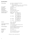
2 specifications frequency range: usa: 100 khz ~ 1299.995 mhz (cellular blocked) exp: 100 khz ~ 1299.995 mhz (frequency range is varied per local law. Ask your yaesu dealer for details for frequency range in your country.) receiving mode: am/fm/wfm circuit type: triple super-heterodyne memory channe...
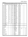
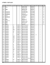
3 exploded view & miscellaneous parts no. Vxstd p/n description qty. U07240307 panhead screw m2x4b#3 2 u9900119 taptite screw m2x5b#3 2 u07125301 panhead screw m1.7x2.5#3 3 À Á vxstd p/n description qty. S6000335 hand strap 1 ra014370b belt clip 1 u9900097 binding head screw m3x5.5b 1 À À Á Á s80019...
Exploded view & miscellaneous parts 4 note:.
5 circuit description vr-120d separates into two substrate blocks. It is rf unit and cntl • af unit. Att, ant band path filter, bar ant for am, rfamp, 1st • 2ndmix, 2ndif-amp, 3rdif-detic, pll, 1st • 2nd-vco, amdet circuit are had by the rf unit. Also, the cntl • af unit has a cpu, lcd, a power, aud...
6 circuit description note:.
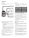
7 alignment introduction the vr-120d has been carefully aligned at the factory for the specified performance across the amateur band. Realignment should therefore not be necessary except in the event of a component failure. All component replacement and service should be performed only by an authori...
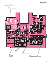
8 alignment test setup set up the test equipment as shown below for receiver alignment. Pll reference frequency adjustment r disable the battery save; m press the [scn] key while press and holding the [func] key. M rotate the dial knob to select the display to " sav e ." m rotate the dial knob while...
9 alignment c305 pll reference frequency adjust tp3 vco vcv: dc voltmeter tp1 pll reference frequency adjust: frequency counter l229 fm discriminator adjust tp2 rf voltege: dc voltmeter alignment points.
10 alignment r tune the receiver to 448.250 mhz. R press and hold the [scan] key for 2 seconds, the rotate the dial knob to select the display to " su ." r press and hold the [scan] key for 2 second while press and holding the [func] key. " sql set " will appears on the display. Sounds a beep. Sql l...
11 alignment r press the [bnd(p)] key while press and holding [func] key. " s m et + " will appear on the display. R press the [v/m] key while press and holding [func] key. Sounds a beep. R reduce the ssg output level to -5 dbµ. R press the [scan] key while press and holding [func] key. " s m et 2 "...
13 block diagram.
14 block diagram note:.
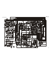
15 cntl•af unit circuit diagram usa b1 b2 r113 --- 0 ---.
16 cntl•af unit note:.
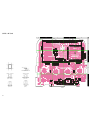
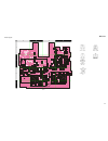
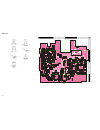
17 cntl•af unit side a a b c d e 1 2 3 4 parts layout rn5vl20a (b0) (q112) umg2n (g2) (q113) dta144ee (16) (q114) dtc144ee (26) (q131, 142) xc6371a351pr (a35) (q116) ta31056f (q123) 2sa1588y (zy) (q124, 125, 128) umw1 (w1) (q126, 127) umx2n (x2) (q130) 1ss382 (a1) (q129) xc6201p322pr (p32) (q118) dt...
18 cntl•af unit side b e d c b a 1 2 3 4 hd6433837sd (q101) 1ss382 (a1) (q102, 103, 104) 2sc4617 (br) (q107, 110) rb706f-40t106 (3j) (q120, 121) at24c64n-10si1.8sl722a (q115) 2sd1615 (gk) (q136).
19 cntl•af unit pcb with component (w/ lcd ass'y, shield case, cushion, contact c) s8101164 usa pcb with component (w/ lcd ass'y, shield case, cushion, contact c) s8101165 b1 pcb with component (w/ lcd ass'y, shield case, cushion, contact c) s8101166 b2 c101 chip cap. 47pf 50v ch grm39ch470j50pt k22...
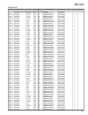
20 cntl•af unit description value v/w tol. Vxstd p/n mfr’s desig vers. Ref. Lot. Lay adr q116 ic xc6371a351pr g1093343 1- d4 q117 diode rb520s-30te61 g2070822 1- d4 q118 ic xc6201p322pr g1093624 1- d3 q120 diode rb706f-40t106 g2070824 1- c4 q121 diode rb706f-40t106 g2070824 1- c4 q123 ic ta31056f(tp...
21 cntl•af unit description value v/w tol. Vxstd p/n mfr’s desig vers. Ref. Lot. Lay adr r150 chip res. 1k 1/16w 5% rmc1/16 102jatp j24185102 1- r151 chip res. 1k 1/16w 5% rmc1/16 102jatp j24185102 1- r152 chip res. 1k 1/16w 5% rmc1/16 102jatp j24185102 1- r153 chip res. 10k 1/16w 5% rmc1/16 103jatp...
22 cntl•af unit note:.
23 rf unit circuit diagram.
24 rf unit note:.
25 rf unit side a a b c d 1 2 3 4 parts layout 1ss364 (bf) (q205, 213, 215) µpc2757t (c1y) (q218) dta144ee (16) (q225) 2sj144y (vy) (q227) 2sc5010 (83) (q214) 2sc4915y (qy) (q220) 2sc4617r (br) (q233) 2sc5006 (24) (q240, 241).
26 rf unit side b 1 2 3 4 d c b a 1ss364 (bf) (q208, 209, 222, 223) dtc144ee (26) (q203, 224, 226) 2sc5006 (24) (q211, 216, 217, 219, 239) 2sc4617r (br) (q234) ta31136fn (q221) umx2n (x2) (q231) mb15f02pfv (q235) 2sk1580 (g13) (q236).
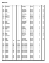
27 rf unit pcb with component (w/ bar antenna ass'y, shield case) s8101168 c201 chip cap. 0.01uf 25v b grm39b103k25pt k22144803 1- c202 chip cap. 0.01uf 25v b grm39b103k25pt k22144803 1- c203 chip cap. 0.01uf 25v b grm39b103k25pt k22144803 1- c204 chip cap. 0.01uf 25v b grm39b103k25pt k22144803 1- c...
28 rf unit description value v/w tol. Vxstd p/n mfr’s desig vers. Ref. Lot. Lay adr c267 chip cap. 0.01uf 25v b grm39b103k25pt k22144803 1- c268 chip cap. 0.01uf 25v b grm39b103k25pt k22144803 1- c269 chip cap. 0.01uf 25v b grm39b103k25pt k22144803 1- c270 chip cap. 0.01uf 25v b grm39b103k25pt k2214...
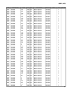
29 rf unit description value v/w tol. Vxstd p/n mfr’s desig vers. Ref. Lot. Lay adr c338 chip cap. 0.001uf 50v b grm39b102k50pt k22174821 1- c339 chip cap. 47pf 50v ch grm39ch470j50pt k22174227 1- c340 chip cap. 47pf 50v ch grm39ch470j50pt k22174227 1- c342 chip cap. 0.01uf 25v b grm39b103k25pt k221...
30 rf unit description value v/w tol. Vxstd p/n mfr’s desig vers. Ref. Lot. Lay adr q203 transistor dtc144ee tl g3070075 1- d2 q204 diode 1ss371(tph3) g2070728 1- c3 q205 diode 1ss364(te85r) g2070730 1- d2 q206 diode 1ss371(tph3) g2070728 1- d2 q207 diode 1ss371(tph3) g2070728 1- d2 q208 diode 1ss36...
31 rf unit description value v/w tol. Vxstd p/n mfr’s desig vers. Ref. Lot. Lay adr r226 chip res. 2.2k 1/16w 5% rmc1/16 222jatp j24185222 1- r227 chip res. 6.8k 1/16w 5% rmc1/16 682jatp j24185682 1- r228 chip res. 10k 1/16w 5% rmc1/16 103jatp j24185103 1- r229 chip res. 0 1/16w rmc1/16 000jatp j241...
32 rf unit description value v/w tol. Vxstd p/n mfr’s desig vers. Ref. Lot. Lay adr r294 chip res. 15k 1/16w 5% rmc1/16 153jatp j24185153 1- r295 chip res. 100k 1/16w 5% rmc1/16 104jatp j24185104 1- r296 chip res. 220k 1/16w 5% rmc1/16 224jatp j24185224 1- r297 chip res. 1k 1/16w 5% rmc1/16 102jatp ...
33 rf unit.
34 rf unit printed in japan. Copyright © 2002 vertex standard co., ltd. All rights reserved no portion of this manual may be reproduced without the permission of vertex standard co., ltd..

