- DL manuals
- Yamaha
- Recording Equipment
- CS1D
- Service Manual
Yamaha CS1D Service Manual
SERVICE MANUAL
PA
011508
CONTENTS
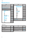
REVISED PAGE LIST ··························································· 2-1
SPECIFICATIONS ································································· 3-1
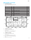
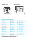
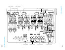
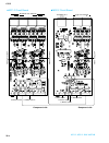
PANEL LAYOUT···································································· 3-3
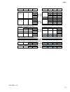
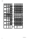
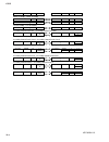
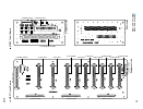
CONNECTOR CIRCUIT DIAGRAM ········································· 4
DISASSEMBLY PROCEDURE··············································· 15
LSI PIN DESCRIPTION ·························································· 31
IC BLOCK DIAGRAM ····························································· 39
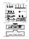
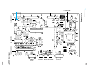
CIRCUIT BOARDS ································································· 45
INSPECTION ·········································································· 98
TEST PROGRAM ································································· 103
BLOCK DIAGRAM ································································ 126
CONTROL SURFACE
HAMAMATSU, JAPAN
Copyright (c) Yamaha Corporation. All rights reserved. PDF-K-
****
'01.03
Summary of CS1D
Page 1
Service manual pa 011508 contents revised page list ··························································· 2-1 specifications ································································· 3-1 panel layout···································································· 3-3 connector circ...
Page 2: Revised Page List
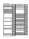
Cs1d 2-1 revised page list specifications connector circuit diagram disassembly procedure lsi pin description ic block diagram circuit boards sto1,sto2,ps2hp mtcpu mb22 mio cio sti aei cnds2,pnis4 cnds1,lampvr,lcdc pnc2,pnm4 ada2 mo1-2,mo2-2 cnds3,lcdif pcif pnis3,pnm3 mtg,mti eif ccas item 3-1 4,5,...
Page 3
Cs1d 2-2 mb21 circuit diagram 002 mb22 circuit diagram mio circuit diagram 002 003 004 cio1 circuit diagram 2/2 sti circuit diagram 2/2 aei circuit diagram 005 sto1 circuit diagram mo1-2 circuit diagram mo2-2 circuit diagram pnc1 circuit diagram 002 003 005 006 008 009 010 eif,ccas circuit diagram 0...
Page 4
Cs1d 2-3 warning: chemical content notice! The solder used in the production of this product contains lead. In addition, other electrical/electronic and/or plastic (where applicable) components may also contain traces of chemicals found by the california health and welfare agency (and possibly other...
Page 5: Specifications
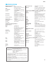
Cs1d 3-1 specifications important notice for the united kingdom connecting the plug and cord important. The wires in this main lead are coloured in accordance with the following code: blue: neutral brown: live as the colours of the wires in the main lead of this apparatus may not correspond with the...
Page 6
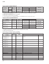
Cs1d 3-2 analog input characteristics input terminals gain actual load impedance for use with nominal input level nominal max. Before clip connector talkback in 1, 2 *3. *5. 2-track in analog 1, 2 *4. -44 db +10 db – 3 k Ω 10 k Ω 50–600 Ω mics & 600 Ω lines 600 Ω lines xlr-3-31 type (balanced) *1. X...
Page 7: Panel Layout
Cs1d 3-3 panel layout note: see operation manual for details. Input/output terminals format level connector type quantity control i/o engine a1in, 1out, 2in, 2out engine b1in, 1out, 2in, 2out console 1in, 1out, 2in, 2out dc power input – – -0.225 v–-1.825 v dc 60 v bnc connector 68p 12 kn-27-32s 27p...
Page 8: Connector Circuit Diagram
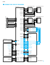
Kec-92541-2 7 6p pni1(cn803) 6p cnds1(cn101) 16p 16p cnds1(cn105) cnds1(cn106) 6p cnds1(cn102) 16p 16p cnds1(cn107) cnds1(cn108) 6p 16p 16p 6p cnds3(cn503) 16p 16p cnds3(cn507) cnds3(cn508) incpu(cn4) incpu(cn5) incpu(cn1) 12p 12p pnc2(cn104) 16p 16p 12p 12p pnc2(cn106) 12p pnc2(cn103) 6p cnds3(cn50...
Page 9
2p 2p 4p cn18 cn12 cn13 6p 2p cn10 cn14 6p cn11 2p cn15 6p cn2 6p cn3 6p 6p 13p cn100 cn103 cn104 6p 6p 16p 16p 16p 16p cn101 cn102 cn105 cn106 cn107 cn108 50p 40p 40p 40p cn1 cn6 cn5 cn4 100p 100p 100p 100p 100p 100p 100p 100p 100p 5p 5p cn101 cn2 cn1 cn1 cn200 cn100 cn2 cn2 cn100 cn100 cn100 [engi...
Page 10
Cs1d 6 to cnds3(cn65) 6p 6p cn31 cn34 6p cn30 6p cn35 8p cn41 6p 2p cn39 cn32 4p cn38 2p 4p 4p cn36 cn40 cn37 2p cn33 cn204 cn207 4p cn201 cn202 2p cn200 12p 12p 12p 4p cn301 to cnds3(cn60) ** • bottom assy(under the assy control panel mas/outsel/insel) 4p cn13 6p 6p 4p cn5 cn6 cn11 2p cn23 2p 6p cn...
Page 11
Cs1d 7 6p 2p cn60 cn68 8p 4p 4p cn67 cn62 2p 6p cn61 cn65 cn66 4p 4p 4p 6p cn501 cn502 cn506 cn505 4p 4p 4p 6p 5p 5p cn507 cn508 cn500 6p cn503 cn509 cn510 6p cn504 16p 16p 16p 16p cn110 cn111 cn114 cn113 cn101 cn101 40p cn102 40p cn103 cn104 cn105 cn106 cn107 cn108 cn109 cn110 10p 10p 10p 10p 12p 1...
Page 12
Cs1d 8 • front assy 6p 8p cn601 cn602 • meter assy cn4 9p cn1 cn5 12p 8p cn6 9p cn5 9p cn4 cn3 12p 8p cn3 cn5 9p 8p cn1 cn2 12p 14p 9p cn2 cn2 cn1 • lcd assy 2p cn401 3p 5p cn301 cn302 cn303 12p 14p 15p lcd 41p 3p cn304 cn3 cn1 cn2 10p 10p [mouse] [keyboard] [monitor a] [monitor b] lcd- backlight **...
Page 13
Cs1d 9 • assy control panel mas 4p fader 2p 7p cn100 cn953 cn954 cn950 cn955 40p 40p 40p 20p 4p 3p 7p cn16 cn32 cn1 4p 3p 7p cn17 cn33 cn2 4p 3p 7p cn18 cn34 cn3 4p 3p 7p cn19 cn35 cn4 4p 3p 7p cn20 cn36 cn5 4p 3p 7p cn21 cn37 cn6 4p 3p 7p cn22 cn38 cn7 4p 3p 7p cn23 cn39 cn8 40p 40p 40p 20p cn15 cn...
Page 14
Cs1d 10 • assy control panel outsel cn101 cn105 100p cn1 cn2 cn9 4p 3p 7p cn34 cn8 cn2 40p 22p 12p 40p 22p 12p cn26 cn13 cn41 8p cn27 4p 3p 7p cn33 cn7 cn1 8p cn25 4p 3p 5p cn21 cn12 cn6 4p 3p 5p cn20 cn11 cn5 cn3 cn9 4p 3p 7p cn36 cn10 cn4 8p cn32 4p 3p 7p cn35 8p cn30 cn701 cn200 cn200 cn602 cn301...
Page 15
Cs1d 11 • assy control panel insel 4p 2p 5p cny1 3p cnx1 cn805 cn801 cn803 cn804 cn802 12p 12p 26p 40p 40p cn804 cn803 cn800 cn802 cn801 12p 12p 22p 40p 40p 4p 3p 5p cn17 3p cn16 12p 12p 26p 40p 40p 12p 12p 22p 40p 40p cn2 cn1 cn15 cn14 cn6 cn10 cn12 cn8 cn13 cn4 cn9 cn7 cn300 cn301 8p 5p cn302 3p c...
Page 16
Cs1d 12 • assy control panel in cn800 cn801 cn802 40p 40p 40p cn44 cn28 cn7 40p 40p 40p cn2 cn6 cn3 cn43 cn46 cn31 cn13 cn45 cn48 cn37 cn16 cn47 cn50 cn40 cn22 cn49 cn52 cn29 cn8 cn51 cn54 cn32 cn14 cn53 cn56 cn38 cn17 cn55 cn58 cn30 cn9 cn57 4p 3p cn60 cn33 cn15 8p cn59 4p 3p cn62 cn41 cn23 8p cn61...
Page 17
Pw1d (input a) pw1d – bottom assembly 11–20 22–24 26–27 3 1,2,4–10 27 power unit 1–10 1–3 1–2 1–9 9 pw1d (input b) 11–20 22–24 26–27 3 1,2,4–10 27 bottom assembly – assembly control panel insel cs ada2 cn104 1–4 4 4 5–8 cs phnab2 cn300 5–8 4 5–8 cs ada2 cn105 1–4 4 4 5–8 bottom assembly – lcd assemb...
Page 18
Cs1d 14 power unit cn15 1–4 4 cn16 4 1–4 cs cnds2 cn41 1–4 8 5–8 power unit cn17 1–4 4 cn18 4 1–4 cs cnds3 cn65 1–4 8 5–8 power unit cn19 1–2 6 3–6 cs cnds2 cn39 1–2 2 cs cnds3 cn66 4 1–4 cn34 power unit 4–6 7–9 1–3 4–6 7–9 1–3 9 cn35 9 cs cnds1 cs cnds2 cs cnds3 cs cnds1 1–3 1–3 4–6 1–3 6 cn11 6 cn...
Page 19
Cannon conector meter assembly – meter assembly 3–4 4 (cn33–43) cs drn 1–2 2 cn101 lcd assembly – lcd assembly 1–2 3 cs lcdc 1–2 2 cn401 cannon conector 3–4 4 cs rds 1–2 2 cn101 cn3 lcd-backlight assembly control panel mas – assembly control panel mas a b 2 mt fader 1 3 3 cn32 cs mscpu (cn2–6) assem...
Page 20: Disassembly Procedure
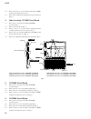
Fig. 1 control panel assembly in 13~24 ch control panel assembly master control panel assembly outsel lcd assembly control panel assembly insel control panel assembly in 1~12 ch control panel assembly in 37~48 ch control panel assembly in 25~36 ch [680k] [680k] [680k] [680b] [680j] [680j] [680j] [68...
Page 21
5. Cs pnm3 circuit board 5-1 remove the control panel assembly (master). (see procedure 1.) 5-2 remove the two (2) screws marked [280]. (fig. 3) 5-3 remove the two (2) switch knobs marked [c]. (fig. 3) 5-4 remove the two (2) screws marked [275]. The cs pnm3 circuit board can then be removed. (fig. 2...
Page 22
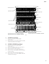
Fig. 3 control panel master encoder knob x36 switch knob c switch knob a x24 switch knob c switch knob b x12 switch knob b x12 fader knob x12 switch knob d [280] [280] [280] [280] [330] [220] x24 [220]: flat head screw 3.0 x 6 mfzn2bl (ec030030) [280]: flat head screw 3.0 x 16 mfzn2bl (vl668700) [33...
Page 23
Cs1d 18 [170a] [190] [190] [190] [170a] [247b] [247a] [248b]x2 [210] [210] [248a]x2 [500]x4 [490] [170b] x10 fig. 4 cs pnis1 cs iscpu protect,p.C.B. Spacer switch knob a switch knob b fader knob fader assembly cs pnis2 cs pnis4 cs pnis3 [170]: bind head screw 3.0x6 mfzn2bl (eg330360) [190]: bind hea...
Page 24
Fig. 5 switch knob a x24 fader knob x12 fader assembly spacer x7 encoder knob x36 cs pni1 cs incpu cs pni2 [210] x24 [130] x36 [170] [150] [205] x12 [130]: hexagonal nut 7.0 10x2 mfzn2bl (es200180) [150]: bind head screw 3.0x6 mfzn2bl (eg330360) [170]: bind head screw 3.0x6 mfzn2bl (eg330360) [205]:...
Page 25
14. Fader assembly, cs pni2 circuit board 14-1 remove the control panel assembly (in12, in24, in36, in48). (see procedure 1.) 14-2 remove the fader knob. (fig. 5) 14-3 remove the two (2) screws marked [210]. The fader assembly can then be removed. (fig. 5) 14-4 remove the screw marked [205]. The cs ...
Page 26
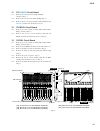
Fig. 7 fader assembly b x2 fader assembly a x4 set screw b encoder assembly protect,p.C.B. Set screw a cs pnos1l cs pnos1c cs pnos3 cs pnos2 cs pnos5 cs pni2 cs oscpu cs pni2 cs pnos1r cs pnos6 [860]x5 [370a] [836a] [275] x6 [180b] x5 [180a] x8 [180c] x3 [836b] [880] [370b] [370a] [180]: bind head s...
Page 27
20. Cs hmvolb2 circuit board 20-1 remove the control panel assembly (out sel). (see procedure 1.) 20-2 remove the two (2) knobs marked [c]. 20-3 remove the two (2) hexagonal nuts marked [c]. The cs hmvolb2 circuit board can then be removed. (fig. 6, fig. 7) 21. Cs pnos3 circuit board 21-1 remove the...
Page 28
Fig. 8 [150] [30] [50] cs crdc1 cs crdc2 [150]: bind head screw a3.0x6 mfzn2bl (vp156600) [30]: bind head screw 3.0x6 mfzn2bl (eg330360) [50]: bind head screw 3.0x6 mfzn2bl (eg330360) cs1d 23 25-3 remove the hexagonal nut marked [d]. The encoder assembly can then be removed. (fig. 6, fig. 7) 26. Cs ...
Page 29
34. Cs cnds1, cs mtcpu circuit board 34-1 remove the control panel assembly (in12, in24). (see procedure 1.) 34-2 remove the six (6) screws marked [826]. The cs cnds1 circuit board can then be removed. (fig. 11) 34-3 remove the eight (8) screws marked [780]. The cs mtcpu circuit board can then be re...
Page 30
Fig. 11 cs pnc2 cs ada2 cs cnds3 cs cnds2 cs mtcpu cs cnds1 [520]x7 [510]x5 [860]x4 [828]x6 [840]x4 [820]x9 [480]x2 [490]x2 [780]x8 [880]x8 [826]x6 [450] [460] [450]: bind head tapping screw-b a4.0x8 mfzn2bl (vc688800) [460]: bind head tapping screw-b 3.0x6 mfzn2bl (ep600230) [480]: bind head tappin...
Page 31
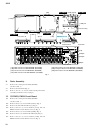
Fan assembly 1 fan assembly 2 cannon assembly cannon assembly fig. 13 [c50] [c50] [c50] [a70] [370] [40] [40] [370] [350] [370] [140] [330] [80] cs mt2 cs mt1 cs mt3 cs drn cs drs cs drl [40]: bind head tapping screw-b 3.0x6 mfzn2bl (ep600230) [80]: bind head tapping screw-b 3.0x6 mfzn2bl (ep600230)...
Page 32
Mo22-card assembly mo12-card assembly sto-card assembly aei-card assembly sti-card assembly cio-card assembly mio-card assembly ad2-card assembly fig. 14 [660]x2 [626]x2 [c] [c] [b]x2 [a]x2 [640]x2 [560]x4 [540]x8 cs1d 27 43. Cs drl circuit board 43-1 remove the cannon assembly. (see procedure 42.) ...
Page 33
Cmu1 fig. 17 battery vn103500 vn103600(battery holder for vn103500) notice for back-up battery removal push the battery as shown in figure, then the battery will pop up. Druk de batterij naar beneden zoals aangeven in de tekening, de batterij springt dan naar voren. Battery battery holder cmu2-card ...
Page 34
Fig. 19 cs mb23 [500c] [500c]: bind head tapping screw-b 3.0 x 6 mfzn2bl (ep600230) cs1d 29 49. Cs mb21, mb22 circuit board 49-1 remove the control panel assembly (in sel, in12, in24). (see procedure 1.) 49-2 remove the rear panel (a). (see procedure 38.) 49-3 remove all the card assembly in the pro...
Page 35
Cs1d 30 52. Cs ps2hp circuit board 52-1 remove the four (4) screws marked [140]. The phj angle can then be removed. (fig. 21) 52-2 remove the two (2) hexagonal nuts marked [30], the two (2) screws marked [50] and the screw marked [60]. Remove the cs ps2hp circuit board on the phj angle. (fig. 21) cs...
Page 36: Lsi Pin Description
Pin no. I/o function name pin no. I/o function name 1 2 3 4 5 6 7 8 vss mclk dm0 dm1 res wcin din v dd i i i i i i ground master clock input din/bclk/wclk format select dm1,dm0=0,0 dsp,ldsp (64 bit,lsb first) dm1,dm0=0,1stereo,dsp (64 bit,msb first) dm1,dm0=1,0 dsp2 (128 bit,msb first) dm1,dm0=1,1 b...
Page 37
Pin no. I/o function name pin no. I/o function name 1 2 3 4 5 6 7 8 9 10 11 12 13 14 dvss dvdd mclk /pd bick sdata lrck smute//cs dfs dem0/cclk dem1/cdti dif0 dif1 dif2 - - i i i i i i i i i i i i digital ground digital power supply master clock power down mode audio serial data clock audio serial d...
Page 38
Cs1d 33 pin no. I/o function name pin no. I/o function name 1 2 3 4 5 6 7 8 9 10 11 12 13 14 15 16 17 18 19 20 21 22 23 24 25 26 27 28 29 30 31 32 33 34 35 36 37 38 39 40 41 42 43 44 45 46 47 48 49 50 51 52 53 54 55 56 57 58 59 60 61 62 63 64 65 66 67 68 69 70 71 72 /wrhh /dack0/pe14 /wrhl cashh/pa2...
Page 39
Cs1d 34 pin no. I/o function name pin no. I/o function name 1 2 3 4 5 6 7 8 9 10 11 12 13 14 15 16 17 18 19 20 21 22 nc nc txd clk res nc /dsr /rts /dtr nc nc nc /rxclk vdd ic d0 d1 d2 d3 rxd gnd nc o i i i o o i i/o i/o i/o i/o i no connection serial data output master clock reset no connection dat...
Page 40
Cs1d 35 pin no. I/o function name pin no. I/o function name 1 2 3 4 5 6 7 8 9 10 11 12 13 14 15 16 17 18 19 20 21 22 23 24 25 26 27 28 29 30 31 32 33 34 35 36 37 38 39 40 syncati mccti mcbti vcc gnd mcati gnd siat0 siat1 siat2 siat3 ati gnd ato soat3 soat2 soat1 soat0 vcc gnd mcato gnd mcbto mccto s...
Page 41
Pin no. I/o function name pin no. I/o function name 1 2 3 4 5 6 7 8 9 10 11 12 13 14 data0 data1 data2 data3 gnd data4 data5 data6 data7 ale cs_n suspend clkout int_n i/o i/o i/o i/o - i/o i/o i/o i/o i i i/o o o bit 0 of bi-directional data. Bit 1 of bi-directional data. Bit 2 of bi-directional dat...
Page 42
Cs1d 37 pin no. I/o function name pin no. I/o function name 1 2 3 4 5 6 7 8 9 10 11 12 13 14 15 16 17 18 19 20 21 22 23 24 25 26 27 28 29 30 31 32 33 34 35 36 37 38 39 40 41 42 43 44 45 46 47 48 49 50 51 52 53 54 55 56 57 58 59 60 61 62 63 64 65 66 67 68 69 70 71 72 73 74 75 76 77 78 79 80 81 82 83 ...
Page 43
Cs1d 38 pin no. I/o function name pin no. I/o function name 1 2 3 4 5 6 7 8 9 10 11 12 13 14 15 5v 5v a_pgm a_vcc /a_vcc /a_vcc 12v avpp avcc avcc avcc gnd nc /shdn 3.3v i i i i i i i o o o o - - i i card power (5 v) card power (5 v) avpp voltage control avpp voltage control avpp voltage control avp...
Page 44: Ic Block Diagram
Ic block diagram cs1d 39 hd74lv02afpel (is000200) quad 2 input nor hd74lv04afpel (is000400) hd74ls06fpel (xh610a00) sn74ls06nsr (xp985a00) hex inverter hd74lv08afpel (is000800) quad 2 input and hd74lv11afpel (is001100) triple 3 input and hd74lv14afpel (is001400) hex inverter hd74hc30fptl (xq970a00) ...
Page 45
Cs1d 40 hd74lv125afpel (is012500) quad 3-state bus buffer sn74lv138ansr (is013810) 3 to 8 demultiplexer sn74lv139ansr (is013910) dual 2 to 4 demultiplexer sn74lv164ansr (is016410) 8-bit shift register hd74lv244afpel (is024400) octal 3-state bus buffer hd74lv245afpel (is024500) tc74vhct245af (xv242a0...
Page 46
Cs1d 41 sn75124nsr (xv930a00) triple line receiver sn75c1168nsr (xu073a00) line driver / receiver sn74lv4052ansr (is405210) differential 4-channel multiplexer/demultiplexer tc74lvx4245fs (xu229a00) dual supply octal bus transceiver am26ls31cnsr (xu996a00) quad line driver ds26c32atm (xq544a00) quad ...
Page 47
Cs1d 42 tc74hc238af (xt163a00) 3 to 8 line decoder ta7291s (xf557a00) motor driver driver tb62705cf (xv013a00) led driver 1 2 3 4 5 6 7 a b c g2b g1 y7 gnd g2a 16 15 14 13 12 11 ycc y0 y1 y2 y3 y4 y5 8 9 10 y6 1 2 a 16 vcc 15 y0 4 g2a 5 g2b 6 g1 7 y7 8 gnd select inputs enable inputs b 3 c 14 y1 13 ...
Page 48
Cs1d 43 td62m8600f (xv014a00) source driver dp8392cn (xw278a00) cti max202cse (xp113a00) rs-232c transceiver 1 2 3 cd+ rx+ 4 v ee 5 v ee 6 rx– tx+ tx– 7 cd– 16 15 14 cds rxi 13 v ee 12 rr– 11 rr+ 10 8 9 gnd hbe txo coax cable rxi cds hbe txo gnd date buffer sense buffer receiver equalizer and amplif...
Page 49: Circuit Boards Contents
Cs1d 44 circuit boards contents ad1890jp (xv453a00) asrc 917090 (xk866a00) ha serial in serial out accum mult fifo coef rom clock tracking 3 4 2 1 28 27 26 25 24 23 22 21 20 19 18 17 16 15 14 13 12 11 10 9 8 7 6 5 wclk - i bclk - i data - i mclk gpdlys setlslw gnd bclk - o wclk - o data - o vdd gnd ...
Page 50: Circuit Boards
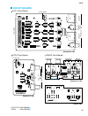
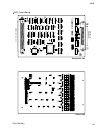
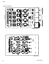
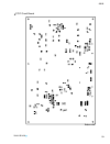
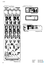
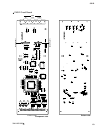
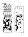
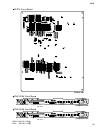
3na-v454540 component side component side component side pattern side to mb21-cn7 to sto2-cn101 aes/ebu 1 2 coaxial stereo out digital aes/ebu coaxial 3na-v504660 ps2hp: sto1,sto2: sto1 circuit board sto2 circuit board ps2hp circuit board word clock mouse keyboard monitor a monitor b to ada2-cn302 t...
Page 51
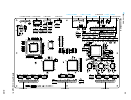
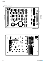
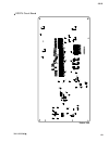
3na-v411320 component side to mb21-cn4 2 mtcpu circuit board to mb21-cn5 to mb21-cn6 to mb21-cn1 to mo1_2-cn405 to mo2_2-cn604 to mo2_2-cn602 to mo1_2-cn400 to mt1-cn2 to mt2-cn2 to mt2-cn1 to pn2-cn109 to cnds1-cn100 to ada2-cn303 to mb22-cn503 cs1d 46.
Page 52
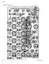
3na-v411320 pattern side 2 mtcpu circuit board cs1d 47.
Page 53
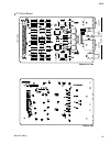
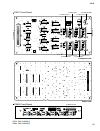
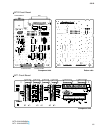
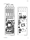
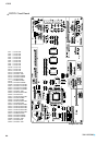
Mb22: 3na-v454540 mb21: 3na-v411330 component side component side pattern side to mtcpu-cn11 to cndc1-cn104 to cnds1-cn103 to mtcpu-cn10 to mtcpu-cn12 to mtcpu-cn14 1 mb21 circuit board mb22 circuit board to sto1-cn1 to ae1-cn1 to sti-cn200 to cio-cn2 to cio-cn2 to mio-cn100 to mio-cn100 to mio-cn10...
Page 54
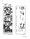
3na-v438190 component side pattern side to mb21-cn15,14,13,12 digital i/o enginea, b 4 mio circuit board cs1d 49.
Page 55
3na-v438180 component side pattern side to mb21-cn10,11 digital i/o console 3 cio circuit board cs1d 50
Page 56
3na-v411300 component side pattern side to mb21-cn9 1 aes/ebu coaxial 2tr in digital aes/ebu coaxial 2 4 sti circuit board cs1d 51.
Page 57
3na-v438150 component side pattern side to mb21-cn8 aes/ebu 3 aes/ebu 4 2tr in digital aes/ebu 5 aes/ebu 6 3 aei circuit board cs1d 52.
Page 58
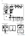
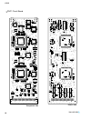
Component side component side pattern side cn30: cn31: cn32: cn33: cn34: cn35: cn36: cn37: cn38: to power unit-cn7 to power unit-cn8 to power unit-cn34,35 to power unit-cn37,38 to power unit-cn9 to power unit-cn10 to power unit-cn36 to power unit-cn40 to power unit-cn11,12 cn39: cn40: cn41: cn200: c...
Page 59
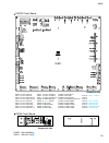
Lampvr, lcdc: 3na-v454540 cnds1: 3na-v506560 component side component side component side pattern side pattern side to incpu-cn5 cnds1 circuit board lcdc circuit board lampvr circuit board from power unit -cn5,6 from power unit -cn11,12 from power unit -cn13,14 from power unit -cn23 from power unit ...
Page 60
Pnm4: 3na-v445280 pnc2: 3na-v454540 component side pattern side to mb23-cn101 to mscpu-cn31 pnc2 circuit board pnm4 circuit board component side to mscpu-cn30 to incpu-cn1 to mtcpu-cn1 to incpu-cn1 to oscpu-cn17 to incpu-cn1 to iscpu-cn3 to cnds3-cn500 to incpu-cn1 3 4 cs1d 55.
Page 61
Cs1d 56-a ada2: 3na-v667370 component side ada2 circuit board to mo2_2-cn606 to mtcpu-cn3 to cutbvl2-cn503 to tb1_2-cn703 to tb1_2-cn702 to hmvolb2-cn204 to hmvola2-cn104 to phnab2-cn300 to ps2hp-cn602 to cutbvl2-cn504 to hmvolb2-cn203 to mo2_2-cn601 to hmvola2-cn103 to cnds2-cn319 to cnds2-cn317 to...
Page 62
Mo1-2, mo2-2: 3na-v667340 component side component side mo1-2 circuit board mo2-2 circuit board l a to mtcpu-cn16 to mtcpu-cn8 r monitor out analog talkback in 2 cue out analog l b r l r to hmvolb2-cn200 to hmvola2-cn100 to cutbvl2-cn500 to ada2-cn103 to mtcpu-cn4 to mtcpu-cn15 to ada2-cn100 to cnds...
Page 63
Lcdif: 3na-v454540 cnds3: 3na-v506570 component side component side pattern side to incpu-cn5 cnds3 circuit board lcdif circuit board to incpu-cn4 to mb23-cn114 to mb23-cn110 to mb23-cn113 from power unit -cn37,38 to lcd to pcif-cn302 to pcif-cn303 to pcif-cn304 from power unit -cn5,6 from power uni...
Page 64
Component side remote rs-422 num key to tpsw-cn101 to ps2hp-cn601 mouse key board svga out pcif circuit board 3na-v451420 7 to crdc1-cn101 to crdc1-cn105 to lcdif-cn301 to lcdif-cn303 to cnds2-cn300 to lcdif-cn302 from mb23-cn108 from mb23-cn109 cs1d 58.
Page 65
3na-v451420 pattern side 7 pcif circuit board cs1d 59.
Page 66
Pnis3: 3na-v411140 pnm3: 3na-v445280 lmy4ad: 3na-v491400 component side component side component side pattern side 2-track in analog l r 1 l r to iscpu-cn16 to mscpu-cn29 2 3 lmy4ad circuit board pnis3 circuit board pnm3 circuit board to mb22-cn502 mscpu-cn46 3 cs1d 60
Page 67
Mt1: 3na-v433370 component side component side pattern side gp1 time code in 2 mtg: 3na-v454540 mtg circuit board mt1 circuit board to cmu2-cn104 to cmu2-cn105 to mt2-cn3 to mt2-cn4 to mt3-cn1 to mt3-cn2 to mtcpu-cn7 to cnds2-cn202 4 cs1d 61.
Page 68
3na-v451320 component side pattern side 2 cmu1 circuit board to mb23-cn106 rc-232-c usb pc control cs1d 62.
Page 69
3na-v451320 component side pattern side out thru in to mtg-cn201 midi 2 cmu2 circuit board to mtg-cn202 to mb23-cn107 cs1d 63.
Page 70
3na-v451380 component side pattern side 5 eif circuit board to mb23-cn104,105 1 in out 2 in out control i/o engine a, b cs1d 64.
Page 71
3na-v504990 component side pattern side 5 ccas circuit board to mb23-cn103 1 in out 2 in out control i/o console cs1d 65.
Page 72
3na-v451350 component side pattern side 3 pnc1 circuit board to mb23-cn102 cs1d 66.
Page 73
3na-v451400 component side pattern side to pcif-cn801 to cnds3-cn505 1 mb23 circuit board to cnds3-cn506 to cnds3-cn502 to cnds3-cn501 to pcif-cn802 to cmu2-cn101 to cmu1-cn101 to efi-cn101 to efi-cn101 to ccas-cn101 to pnc1-cn101 to pnc2-cn102 cs1d 67.
Page 74
Cutbvl2, hmvola2, hmvolb2: 3na-v667380 component side component side to mo2_2-cn605 cutbvl2 circuit board hmvola2 circuit board hmvolb2 circuit board cue out level talkback2 talkback1 phones phones level level to ada2-cn108 to ada2-cn107 component side to ada2-cn307 to ada2-cn308 to phnab2-cn304 to ...
Page 75
Drs: 3na-v470630 drl: 3na-v554710 phnab2: 3na-v667380 drn: 3na-v456620 component side 3 3 1 drn circuit board drs circuit board to fan to cnds2-cn201 lamp component side drl circuit board phnab2 circuit board fan high/low to ada2-cn104,105,300 to hmvolb2-cn206 to hmvola2-cn105 to hmvola2-cn106 lamp ...
Page 76
3na-v433380 component side pattern side to mtcpu-cn5 to mtcpu-cn6 to cnds2-cn204 to mt1-cn1 to mt1-cn5 2 mt2 circuit board cs1d 70
Page 77
3na-v504970 component side pattern side to mt1-cn3 to mt1-cn6 to cnds2-cn207 mt3 circuit board 2 cs1d 71.
Page 78
Pnm2: 3na-v411170 pnm1: 3na-v411160 component side component side to mscpu-cn15 to mscpu-cn28 to mscpu-cn13 to mscpu-cn14 to mscpu-cn16 2 2 pnm1 circuit board pnm2 1/12 circuit board 1 component side to mscpu-cn17 pnm2 2/12 circuit board 2 cs1d 72.
Page 79
To mscpu-cn18 to mscpu-cn19 pnm2: 3na-v411170 pnm1: 3na-v411160 pattern side component side 2 2 pnm1 circuit board pnm2 3/12 circuit board 3 component side pnm2 4/12 circuit board 4 to cnds2-cn302 to cnds2-cn303 cs1d 73.
Page 80
3na-v41170 component side 2 pnm2 5/12 circuit board to mscpu-cn20 5 component side pnm2 6/12 circuit board to mscpu-cn21 6 component side pnm2 7/12 circuit board to mscpu-cn22 7 component side pnm2 8/12 circuit board to mscpu-cn23 8 component side pnm2 9/12 circuit board to mscpu-cn24 9 component si...
Page 81
Crdc2: 3na-v451440 pnos4: 3na-v504670 crdc1: 3na-v451430 component side component side component side pattern side pattern side to pcif-cn201 to pcif-cn202 to oscpu-cn22/23 crdc1 circuit board crdc2 circuit board pnos4 circuit board pc ata storage card b pc ata storage card a 3 cs1d 75.
Page 82
3na-v411180 component side 3 mscpu circuit board cn1: cn2: cn3: cn4: cn5: cn6: cn7: cn8: cn9: cn10: to fader 1/12-vr to fader 2/12-vr to fader 3/12-vr to fader 4/12-vr to fader 5/12-vr to fader 6/12-vr to fader 7/12-vr to fader 8/12-vr to fader 9/12-vr to fader 10/12-vr cn11: cn12: cn13: cn14: cn15:...
Page 83
3na-v411180 pattern side 2 mscpu circuit board cs1d 77.
Page 84
3na-v445280 component side component side to oscpu-cn13 to oscpu-cn41 to oscpu-cn21 to oscpu-cn26 3na-v504670 pnos5: pnos2: 3 pnos2 circuit board pnos5 1/2 circuit board 3 cs1d 78.
Page 85
3na-v445280 pattern side component side to oscpu-cn20 3 3na-v504670 pnos5: pnos2: 3 pnos2 circuit board pnos5 2/2 circuit board cs1d 79.
Page 86
Pnos3,pnos6: 3na-v445280 tb1-2, tb1can2: 3na-v667380 component side component side component side component side to ada2-cn304 to ada2-cn106 to oscpu-cn29 tb1-2 circuit board pnos3 circuit board pnos6 circuit board tb1can2 circuit board to oscpu-cn28 to oscpu-cn31 3 to cnds2-cn315 cs1d 80
Page 87
3na-v445270 component side pattern side to oscpu-cn38 to oscpu-cn15 to oscpu-cn19 2 pnos1r circuit board cs1d 81.
Page 88
3na-v433340 component side pattern side to oscpu-cn14 2 pnos1l circuit board to oscpu-cn24 to oscpu-cn40 to oscpu-cn42 cs1d 82.
Page 89
Pni2: 3na-v411110 pnos1c: 3na-v445280 component side component side to oscpu-cn39 to incpu-cn43,44 to oscpu-cn16 3 2 pnos1c circuit board pni2 1/26 circuit board to incpu-cn45,46 to incpu-cn47,48 to incpu-cn49,50 component side pni2 2/26 circuit board component side pni2 3/26 circuit board component...
Page 90
3na-v411110 2 pni2 6/26 circuit board component side to incpu-cn53,54 pni2 7/26 circuit board component side to incpu-cn55,56 pni2 8/26 circuit board component side to incpu-cn57,58 pni2 9/26 circuit board component side to incpu-cn59,60 pni2 10/26 circuit board component side to incpu-cn61,62 pni2 ...
Page 91
3na-v411110 2 pni2 15/26 circuit board component side to incpu-cn47,48 pni2 16/26 circuit board component side to incpu-cn49,50 pni2 17/26 circuit board component side to incpu-cn51,52 pni2 18/26 circuit board component side to incpu-cn53,54 pni2 19/26 circuit board component side to incpu-cn55,56 p...
Page 92
Pni2: 3na-v411110 iscpu: 3na-v411150 component side cn1: cn2: cn3: cn4: cn5: to fader-mt to fader-vr to pnc2-cn107 to pnis1-cn800 to cnds2-cn205 cn6: cn7: cn8: cn9: to pnis2-cn803 to pnis1-cn801 to pnis2-cn802 to pnis1-cn802 cn10: cn11: cn12: cn13: to pnis2-cn804 to cnds2-cn206 to pnis1-cn804 to pni...
Page 93
Pni2: 3na-v411110 iscpu: 3na-v411150 pattern side 2 2 iscpu circuit board pni2 26/26 circuit board component side pni2 25/26 circuit board component side to oscpu-cn25,33 cn-30,35 to oscpu-cn27,34 cn-32,36 cs1d 87.
Page 94
3na-v433360 component side cn1: cn2: cn3: cn4: cn5: cn6: cn7: cn8: cn9: cn10: cn11: cn12: cn13: cn14: cn15: cn16: cn17: cn18: cn19: cn20: cn21: cn22: cn23: cn24: cn25: cn26: cn27: cn28: cn29: cn30: cn31: cn32: cn33: cn34: cn35: cn36: cn37: cn38: cn39: cn40: cn41: cn42: to fader-mt to fader-mt to fad...
Page 95
3na-v433360 pattern side 0 oscpu circuit board cs1d 89.
Page 96
3na-v411130 component side to iscpu-cn7 to iscpu-cn9 to iscpu-cn4 to iscpu-cn13 2 pnis1 circuit board to iscpu-cn12 cs1d 90
Page 97
3na-v411130 pattern side 2 pnis1 circuit board cs1d 91.
Page 98
3na-v411140 component side to iscpu-cn8 to iscpu-cn10 3 pnis2 circuit board to iscpu-cn15 to iscpu-cn6 to iscpu-cn14 cs1d 92.
Page 99
3na-v411140 pattern side 3 pnis2 circuit board cs1d 93.
Page 100
3na-v411120 component side cn1: cn2: cn3: cn4: cn5: cn6: cn7: cn8: cn9: cn13: cn14: cn15: cn16: cn17: cn18: cn22: cn23: cn24: cn28: cn29: cn30: cn31: cn32: cn33: cn37: cn38: cn39: cn40: cn41: cn42: to pnc2-cn103,104, 105,106 to pni1-cn800 to pni1-cn802 to cnds1-cn105,107 cnds3-cn507,509 to cnds1-cn1...
Page 101
3na-v411120 pattern side 2 incpu circuit board cs1d 95.
Page 102
3na-v411100 component side to incpu-cn2 to incpu-cn6 to incpu-cn3 2 pni1 circuit board cs1d 96.
Page 103
3na-v411100 pattern side to cnds1-cn101,102 cnds-cn503,504 2 pni1 circuit board cs1d 97.
Page 104: Inspection
Cs1d 98 inspection 1. Range of applicability these standards apply to the cs1d. 2. Preparations 2-1. Conditions for details on the connection method, refer to the test program specifications kes-92654. The function generator used for inspection must be the sony tektronix afg310 or equivalent. When u...
Page 105
Cs1d 99 (4) residual noise (al, ar, bl, and br) conditions: 2-track in analog 1l, 1r, 2l, and 2r shorted with 150 Ω . (5) level differences between al and ar and between bl and br the difference in gain measured in (1) must be within the following range. (6) crosstalk between al and ar and between b...
Page 106
Cs1d 100 3-4. Output level difference the gain differences when monitor out al, ar, bl, and br and cue out l and r are measured at 1 khz must be within the following range. 3-5. Phones out al, ar, bl, and br conditions: inspect according to 16. Analog out in the test program specifications kes-92654...
Page 107
Cs1d 101 (4) noise level ein (1 and 2) conditions: input terminal shorted with 150 Ω . However, if the noise level is not in the above tolerance range, this condition must be met: measurement value - (gain at 1 khz)= -126 (5) level differences between 1 and 2 the difference in gain measured in (1) m...
Page 108
Cs1d 102 4. Noise · for details on the connection method etc., refer to the test program specifications kes-92654. · since a 2 track in digital coaxial 1,2 receiver has been selected in 1,2, use a coaxial cable (50 , 50m) for the connection for those terminals. · output 03d oscillation 1 khz to st o...
Page 109
Cs1d 102-a 7. Factory settings · initialization while holding down the left and right switches at the bottom of the track pad, switch on the power switch to start up the syste software use the material provided in 2-2 m, then initialize according to the screen instructions. The knobs not controlled ...
Page 110: Test Program
Cs1d 103 test program a. Preparations for inspection this equipment requires firmware. When there are changes to the manufacturing processes and program for this equipment, it is necessary to write the new firmware to flashrom from a pc. The software used and firmware used and their version numbers ...
Page 111
• method for writing firmware using the dsp1d rs232c port * it is possible to write the cpu firmware from the pc via the rs232c port. This is the method normally used. * refer to "installation directions" in the "pm1d system software" for precautions and other such warnings. 1. Install and set pm1dl...
Page 112
1. Install and set pm1dload with the methods above. 2. Connect a d-sub 9-pin serial cable (cross) and dsp-check (serial communications jig) between the pc and the connector for the sheet to be written as in the figure above. (for the sheet names and connector numbers, see page 103.) 3. Switch on the...
Page 113
B. Inspection method cs1d is controlled by the pm1d inspection pc software and the inspection is carried out autonomously. The inspection configuration diagrams are on the subsequent pages. Locations with instructions for changes have instructions for that inspection item in the pc software, so chan...
Page 114
The pm1d is inspected using pc inspection software. This inspection software is common for ai8/ao8/dsp1d/cs1d. After connecting as shown in the test program specifications for the unit to be inspected (for example cs1d -> see the inspection configuration drawing on the next page), start the pm1d ins...
Page 115
Cs1d midi out midi in pc gpi in pw1d w.Clk i/o oscilloscope func. Generator tc in gpi out usb serial midi thru remote st.Out a/b (coax) 2tr-in 1-2 (coax) st.Out a/b (aes/ebu) 2tr-in 3 (aes/ebu) 2tr-in 3-6 (aes/ebu) 2tr-in 1-2 (aes/ebu) talk back, cue out,moni 2tr-in ana. Trs-phone console engine b e...
Page 116
* for details on inspections 15 and 16, refer to the cs1d overall inspection specifications. To console 2 my8-ae (out 4) phone a l r 4 2ch 4 2ch 2ch cs1d l r digital analog l r phone b auditory inspection phone a/b have the same output. Switch between aes/ebu and coax with the pm1d inspection softwa...
Page 117
Cs1d 109 ng now checking … 1-3.Cs1d-pcif(lcd,rs422),crdc 1-3. Cs1d-pcif(lcd,rs422),crdc lcd,crt: ng ng carda,b: * lcd, crt ng ng example * card a, b ok 1-3.Cs1d-pcif(lcd,rs422),crdc 1-3. Cs1d-pcif(lcd,rs422),crdc lcd,crt: ok carda,b: ok * lcd, crt ok ok please check [lcd] and [crt]. Ok ng * card a, ...
Page 118
Cs1d 109-a [explanation of the lcd screen check items] the patterns shown as 1 through 8 below are repeated every five seconds. Note that the timer is cleared when the mouse pad is touched. Therefore, move the mouse at the screen that you wish to stop. Hhhhhhhhhhhhhhhhhhhhhhhhhhhhhhhhhhhhhhhhhhhhhhh...
Page 119
2-1. Cs1d-cmu1 (cmu-ic115) test checks around the cmu of cmu1. Check item id cmu [00h] ram • data bus 16bit(15-0) • address bus 16bit(16-1) flash (check sum) version dpm • cm bus hi bus l • cm bus tc bus l • cm bus pn bus l • cm bus cn bus l battery 2-2. Cs1d-cmu2 (tcu-ic109) test checks around the ...
Page 120
* remote (cross) ok * tc in ok * remote (straight) ok * midi ok 3. Cs1d-mtg ok 3. Cs1d-mtg tc ic ok remote (cross) ok tc in ok remote (straight) ok midi ok gpi ok * tc ic ok * gpi ok please stop [d24]. Ok please stop [d24] and connect it by [cross serial cable]. Ok replace [cross] serial cable with ...
Page 121
5-1.Cs1d-in 1-12 panel test checks around the in 1-12 panel cpu (ic2). Check item id in [0bh] ram • data bus 16bit(15-0) • address bus 16bit(16-1) flash (check sum) version 5-2.Cs1d-in13-24 paneltest checks around the in 13-24 panel cpu (ic2). Check item id in [0bh] ram • data bus 16bit(15-0) • addr...
Page 122
* ram ok ok ok ok 9. Cs1d-meter panel ok 2-1. Cs1d-meter panel id: meter [0ah] ok ram(ic4): ok version: ok ok dsp5(ic14,ic15): flash(ic2): ok * id meter [0ah] * version latest = ???? * flash * dsp5cpu ok now checking … databus databus 00000000 00000000 pio 00000000 00000000 00000000 00000000 address...
Page 123
* 1 items common to all panels 1. Entering panel diagnostics mode it is possible to check the panel diagnostics for individual panels or for the entire console. Since the diagnostics program is included in the firmware for each panel, it is possible to inspect by entering panel diagnostics mode with...
Page 124
Dark ok ng panel test mode 2 mode 3 mode 1 all all all all all all all all slow fast slow fast slow slow module (13-24) init fast slow slow module ( 1-12) module (25-36) module (37-48) input fast slow slow fast fast fast fast bright master module selected input module selected output module meter mo...
Page 125
Cs1d 116 1) everything but 7x5 led lit up 2) 7x5 leds display in order from the left overall flow 1 line at a time 1 column at a time ( ) 3) faders 4) everything but 7x5 led off 5) repeated for 12 channels all channels lit at the same time in the order given on the left. Encoder outer periphery leds...
Page 126
Cs1d overall flow 1 block all lit mix send checked four at a time (three sets for mix1-12) 1) encoder outer periphery leds lit (in the order in the figure on the right) 2) encoder outer periphery leds lit up one point at a time in the clockwise direction. (mix1, mix2, mix3, and mix4 simultaneously) ...
Page 127
(from here, all columns are lit at the same time in the order written on the left.) 1) one column all lit (except 7x5 leds) 2) 5x7 leds display in order from the left 1 line at a time 1 column at a time ( ) 3) faders 12 columns repeated overall flow cs1d 118 10-3. Pnm test (master module inspection)...
Page 128
Overall flow for all the blocks, after the entire block has been lit up, the check proceeds. Block all lit block all lit block all lit block all lit block all lit four 7-segment leds 1) encoder outer periphery leds lit up one point at a time in the clockwise direction. (all encoders at the same time...
Page 129
Cs1d 120 • inc: current display value incremented 0.1 (maximum = 99.9) • number keys: the corresponding value is displayed in the first position after the decimal point. The switches around selected output channel are displayed as numbers on the channel select 7-segment display unit. • shift: 1 • de...
Page 130
* w.Clk ok 12-1. Cs1d-mio (engine a1)ok 12-1. Cs1d-mio (engine a1) si/so: ok w.Clk: ok id: ok * si/so ok * id ok * msb/lsb ok * 2ch/4ch ok in out a1 b2 please select 68pin ports to check. [to console port] [engine port] ok connect [engine a1] to [to console 1]. Ok cancel the cio port combinations fo...
Page 131
* w.Clk ok 13-1. Cs1d-cio (console 1) ok 13-1. Cs1d-cio (console 1) (select engine port = a1) si/so: ok w.Clk: ok id: 2ch/4ch: ok ok * si/so ok * id ok in out connect [to console 1] to [engine a1] ok cancel the mio port used for the cio check is selected from the pull-down list. When 1 is selected: ...
Page 132
Cs1d 123 on off ok 14-1.Cs1d-dig i/o(coaxial) ok 14-1. Cs1d-dig i/o (coaxial 1-2) w.Clk 75ohm sw: w.Clk: in48khz + 6%: in44.1khz - 10%: jitter48khz: jitter44.1khz: dir2 in/out: led2: coaxial 1 (st.Out a -> 2tr.In 1): coaxial 2 (st.Out b -> 2tr.In 2): * w.Clk 75ohm sw * w.Clk ok ok ok in 48 khz + 6% ...
Page 133
Cs1d 124 ok 14-3.Cs1d-dig i/o(aes/ebu) ok 14-2.Cs1d-dig i/o (aes/ebu 3-6) aes/ebu 3 (st.Out a ->2tr.In 3): aes/ebu 4 (st.Out a ->2tr.In 4): * aes/ebu 3 (st.Out a ->2tr.In 3) * aes/ebu 4 (st.Out a ->2tr.In 4) ok ok * aes/ebu 5 (st.Out b ->2tr.In 5) * aes/ebu 6 (st.Out b ->2tr.In 6) ok ok ok aes/ebu 5...
Page 134
@@@@@@@@e? @@@@@@@@e? @@h? @@h? @@h? @@h? @@h? @@h? @@@@@@@@e?@@@@@@@@?E@@@@@@@@e?@@@@@@@@?E@@@@@@@@e?@@@@@@@@?E@@@@@@@@e?@@@@@@@@?E@@@@@@@@e?@@@@@@@@?E@@@@@@@@e?@@@@@@@@?E@@@@@@@@e?@@@@@@@@?E@@@@@@@@e?@@@@@@@@?E@@@@@@@@e?@@@@@@@@?E@@@@@@@@e?@@@@@@@@?E@@@@@@@@e?@@@@@@@@?E@@@@@@@@e?@@@@@@@@?E@@@@@@@@...
Page 135: Block Diagram
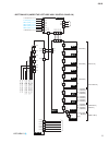
Whole bottom assay assay control panel insole assay control panel mass (fader,mscpu, pnm1,pnm2, pnm3,pnm4) assay control panel outsell front assay (ps2hp) meter assay (drn,drs,fan,lampvr,mt1,mt2,mt3,drl) lcd assay (lcd,lcd- backlight, lcdc,lcdif) 27p [dc power input a] [dc power input b] 27p assay c...
Page 136
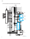
Bottom assy left [engine a] [1] [2] [engine b] [1] [2] [console] [1] [2] power distributor [aes/ebu] [1] [2] [coaxial] [aes/ebu] [3] [4] [5] [6] [1] [2] [75 ] [in] [out] [word clock] [on] [off] [stereo out] [digital] [2tr in digital] [aes/ebu] [coaxial] [aes/ebu] [aes/ebu] [aes/ebu] [aes/ebu] [coaxi...
Page 137
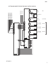
Bottom assy center [2-track in] [analog] [1] [2] [l] [r] [l] [r] [a] [b] [l] [r] [l] [r] [monitor out] [analog] [talkback in 2] [cue out analog] [l] [r] [svga out] [key board] [mouse] [num key] [remote] [rs-422] 27p power unit cpu card 27p p.148 p.148 p.148 p.147 p.146 p.145 power distributor mt1 dr...
Page 138
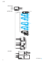
Bottom assy right [in] [out] [thru] [midi] [time code in] [gpi] [usb] [rs-232-c] [pc control] [1] [2] [in] [out] [in] [out] [engine a] [1] [2] [in] [out] [in] [out] [engine b] [1] [2] [in] [out] [in] [out] [console] [control i/o] p.150 p.150 p.151 p.152 p.155 p.149 power distributor pcif cmu2 cmu1 p...
Page 139
Assy control panel in cpu (in) sh7042a sel encoder counter data driver scan driver motor driver sel data buffer buffer buffer led sw x12 fader led sw rotary encoder 7seg ic600~618 16p scan driver data driver matrix circuit matrix buffer matrix dot matrix led buffer in control i/o pni1 pni2 pni2 ic80...
Page 140
Cpu (insel) flash memory sel encoder counter data buffer buffer buffer fader led sw rotary encoder rotary encoder 7seg 7seg scan driver data driver matrix circuit matrix circuit matrix matrix dot matrix led dot matrix led buffer led sw matrix matrix led sw is,os control i/o [monitor a] [monitor b] p...
Page 141
Assy control panel outsel1 rotary encoder scan driver matrix circuit led 7seg matrix sw matrix sw matrix circuit matrix matrix led sw rotary encoder 7seg 7seg scan driver scan driver data driver data driver data driver matrix circuit matrix buffer buffer buffer buffer matrix dot matrix led led cpu (...
Page 142
Assy control panel outsel2 monitor a level monitor b level vol vol vol vol vol monitor a phones monitor b phones monitor a (l) monitor a (r) phones a (r) phones a (l) monitor b (l) monitor b (r) phones b (l) phones b (r) monitor a l monitor a r phones a l phones a r phones a l phones a r monitor b l...
Page 143
Assy control panel master led rotary encoder 7seg scan driver data driver matrix circuit matrix dot matrix led buffer buffer cnds2 supplies the power sw matrix buffer led sw cpu (mas1) sel buffer x12 fader cpu (mas2) encoder counter flash memory data buffer data driver flash memory motor driver scan...
Page 144
Cs1d 135 monitor a monitor b lcd-backlight lcd buffer brightness vol front assy lcd assy pcif supplies the power. Keyboard mouse hp a l out hp a r out hp b l out hp b r out mouse keyboard front,lcd assy pcif pcif lcdc ada2 ps2hp lcdif kec-92540-11 2.
Page 145
Meter assy sw fan fan lamp lamp low speed high speed vol lamp dimmer voltage regulator voltage regulator voltage regulator voltage regulator matrix circuit buffer dot matrix led led matrix scan driver scan driver scan driver data driver data driver data driver matrix circuit buffer buffer buffer led...
Page 146
(bottom assy left) mtcpu cpu (meter) sh7042a ic1 flash memory sram pld (fpga) address decoder i/o port clock system dsp block (see page 209) buffer & transceiver pll for clock generation (dir2 x2) pll for valid detection (dir2 x1) buffer & transceiver xtal (24.576mhz) xtal (22.5792mhz) led drive cir...
Page 147
B 2tr in 1(lr) b 2tr in 2(lr) b 2tr in 5(lr) b 2tr in 6(lr) b 2tr in 3(lr) b 2tr in 4(lr) a 2tr in 1(lr) a 2tr in 2(lr) a 2tr in 5(lr) a 2tr in 6(lr) a 2tr in 3(lr) a 2tr in 4(lr) b digital stereo out a(lr) b digital stereo out b(lr) (bottom assy left) mtcpu -dsp 2tr in 1(digital) [engine a1] 2tr in...
Page 148
Cs1d 139 (bottom assy left) mb21 engine a 1 i/o out audio engine a 1 i/o in audio a fs,etc. Engine a 1 i/o wc engine a 2 i/o in audio engine a 2 i/o wc engine b 1 i/o in audio engine b 1 i/o wc engine b 1 i/o out audio engine b 2 i/o in audio engine b 2 i/o wc console 1 i/o out audio console 1 i/o i...
Page 149
Cs1d 140 (bottom assy left) mio a connector(d-sub half pitch 68p) receiver & buffer dir2 (256fs,etc. Generator, wc detector) engine a 1 i/o in audio engine a 1 i/o in audio engine a 1 i/o in audio engine a 1 i/o wc fs,etc. Fs,etc. A engine a 1 i/o in audio fs,etc. Id id engine a 1 i/o wc engine a 1 ...
Page 150
Cs1d 141 (bottom assy left) cio mb21 buffer & transceiver a connector(d-sub half pitch 68p) receiver & buffer i/o port console 1 i/o in audio console 1 i/o in audio console 1 i/o in audio console 1 i/o wc fs,etc. Fs,etc. A console 1 i/o in audio fs,etc. Id id console 1 i/o wc console 1 i/o wc consol...

