- DL manuals
- Yamaha
- Recording Equipment
- DME32
- Service Manual
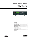
Yamaha DME32 Service Manual
SERVICE MANUAL
PA
011522
HAMAMATSU, JAPAN
1.44K-6661 K
Printed in Japan '00.08
CONTENTS
SPECIFICATIONS ···································································· 3
PANEL LAYOUT ······································································· 5
CIRCUIT BOARD LAYOUT ······················································ 7
DIMENTIONS ··········································································· 8
DISASSEMBLY PROCEDURE················································· 9
LSI PIN DESCRIPTION ·························································· 12
IC BLOCK DIAGRAM ····························································· 19
TEST PROGRAM AND INSPECTION···································· 22
FLASH ROM UPGRADE ························································ 27
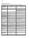
ERROR MESSAGES ······························································ 28
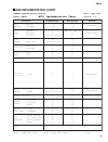
MIDI IMPLEMENTATION CHART ·········································· 31
MIDI DATA FORMAT······························································ 32
CIRCUIT BOARDS ································································· 34
CIRCUIT DIAGRAM AND BLOCK DIAGRAM
DIGITAL MIXING ENGINE
200007**
This document is printed on chlorine free (ECF) paper with soy ink.
Summary of DME32
Page 1
Service manual pa 011522 hamamatsu, japan 1.44k-6661 k printed in japan '00.08 contents specifications ···································································· 3 panel layout ······································································· 5 circuit board layout ··················...
Page 2
Dme32 2 warning: chemical content notice! The solder used in the production of this product contains lead. In addition, other electrical/electronic and/or plastic (where applicable) components may also contain traces of chemicals found by the california health and welfare agency (and possibly other ...
Page 3: Specifications
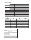
Specifications dme32 3 internal sampling frequency external signal delay configuration memories scene display scene no. Wordclock indicators emergency mode others pc card slot power requirements power consumption dimensions (w x h x d) weight free-air operating temperature storage temperature power ...
Page 4
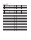
Dme32 4 connector pin assignments pc control (rs232c) pin 1 2 3 4 5 name unused rxd txd dtr gnd in/out — in out out — pin 6 7 8 9 name dsr rts cts unused in/out in out in — pc control (rs422) pin 1 2 3 4 5 name unused rx- tx- tx+ gnd in/out — in out out — pin 6 7 8 9 name rx+ rts cts unused in/out i...
Page 5: Panel Layout
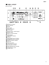
1 6 7 8 9 10 11 12 13 14 15 16 17 18 19 20 21 22 2 3 4 5 1 scene no. Indicator 2 scene edit dots 3 display 4 data wheel 5 inc & dec buttons 6 store button 7 scene recall number keypad 8 recall button 9 48khz & 44.1khz indicators 10 lock indicator 11 emergency indicator 12 usb port 13 component butto...
Page 6
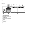
Dme32 6 23 28 29 30 31 32 33 34 35 24 25 26 27 23 ac in connector 24 word clock out connector 25 word clock 75 ohm on/off switch 26 word clock in connector 27 midi in & out ports 28 pc control rs232c/rs422 switch 29 pc control port 30 com port 31 cascade out port 32 cascade in port 33 ground termina...
Page 7: Circuit Board Layout
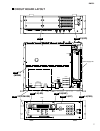
Cn005 cn017 cn018 cn008 cn007 cn010 cn006 cn004 cn012 cn014 cn013 cn011 cn016 cn502 cn501 lcd power supply unit main pnr 3/3(gpi) pnr 1/3 (mymb) pnr 2/3(pcmusb) pnf 3/4(led) pnf 2/4(enc) pnf 1/4(fp) pnf 4/4(psw) circuit board layout dme32 7.
Page 8: Dimentions
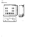
Dme32 8 dimentions w: 480 430 355 d: 375.2 81 81 318 9.5 30 (34) 18 30 43.5 2.2 277.5 132 h: 141.5 unit: mm.
Page 9: Disassembly Procedure
[470] top cover [470] [320a] [320a]: bind head tapping screw-b a4.0x8 mfzn2bl (vc688800) [470]: bind head tapping screw-b a4.0x8 mfzn2bl (vc688800) [320b]: bind head tapping screw-b a4.0x8 mfzn2bl (vc688800) [350]: oval head screw b4.0x10 mfznbl (v6221000) fig. 1 fig. 2 [470] [320b]x4 [350] right si...
Page 10
Dme32 10 [420] [430] [a] [a] pnr [290]: pan head screw 2.6x6 mfzn2bl (vc990500) [420]: bonding screw 3.0x6 mfzn2bl (vs863000) [430]: bonding tapping screw-b 3.0x8 mfzn2bl (vn413300) fig. 3 [290] 3/3(gpi) [290] • lithium battery main [150]: bind head tapping screw-b a4.0x8 mfzn2bl (vc688800) [440]: b...
Page 11
Dme32 11 [30]: bind head tapping screw-b 3.0x6 mfzn2bl (ep600230) [50]: pan head screw 2.6x6 mfzn2bl (vc990500) [60]: bonding screw 3.0x6 mfzn2bl (vs863000) fig. 7 [30a] [30a] [30b] 1/4(fp) [60] [50] [30b] [30c] [30a] lcd [60] pn 2/4(enc) pn 3/4(led) pn 4/4(psw) pn 7-3 pnf1/4(fp) circuit board: remo...
Page 12: Lsi Pin Description
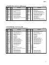
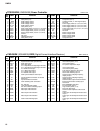
Dme32 12 lsi pin description hd6437042af62f (xy885b00) cpu ································································································· 14 mr-shpc-01 (xw937a00) pc card controller ················································································ 15 sgh609080f-47f ...
Page 13
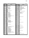
Dme32 13 pin no. I/o function name pin no. I/o function name 1 2 3 4 5 6 7 8 9 10 11 12 13 14 15 16 17 18 19 20 21 22 23 24 25 26 27 28 29 30 31 32 33 34 35 36 37 38 39 40 41 42 43 44 45 46 47 48 49 50 51 52 53 54 55 56 57 58 59 60 61 62 63 64 65 66 67 68 69 70 71 72 gnd /reset /srd /swe0 /swe1 /bs ...
Page 14
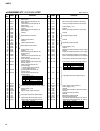
Dme32 14 pin no. I/o function name pin no. I/o function name 1 2 3 4 5 6 7 8 9 10 11 12 13 14 15 16 17 18 19 20 21 22 23 24 25 26 27 28 29 30 31 32 33 34 35 36 37 38 39 40 syncati mccti mcbti vcc gnd mcati gnd siat0 siat1 siat2 siat3 ati gnd ato soat3 soat2 soat1 soat0 vcc gnd mcato gnd mcbto mccto ...
Page 15
Dme32 15 pin no. I/o function name pin no. I/o function name 1 2 3 4 5 6 7 8 9 10 11 12 13 14 15 16 17 18 19 20 21 22 23 24 25 26 27 28 29 30 31 32 33 34 35 36 37 38 39 40 41 42 43 44 45 46 47 48 49 50 51 52 53 54 55 56 57 58 59 60 61 62 63 64 65 66 67 68 69 70 71 72 73 74 75 76 77 78 79 80 81 82 83...
Page 16
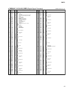
Pin no. I/o function name pin no. I/o function name 1 2 3 4 5 6 7 8 9 10 11 12 13 14 15 16 17 18 19 20 21 22 23 24 25 26 27 28 29 30 31 32 33 34 35 36 37 38 39 40 41 42 43 44 45 46 47 48 49 50 51 52 53 54 55 56 57 58 59 60 61 62 63 64 65 66 67 68 69 70 71 72 73 74 75 76 77 78 79 80 81 82 83 84 85 86...
Page 17
Dme32 17 pin no. I/o function name pin no. I/o function name 1 2 3 4 5 6 7 8 9 10 11 12 13 14 data0 data1 data2 data3 gnd data4 data5 data6 data7 ale cs_n suspend clkout int_n i/o i/o i/o i/o - i/o i/o i/o i/o i i i/o o o bit 0 of bi-directional data. Bit 1 of bi-directional data. Bit 2 of bi-direct...
Page 18
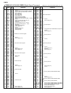
Dme32 18 pin no. I/o function name pin no. I/o function name 1 2 3 4 5 6 7 8 9 10 11 12 13 14 15 5v 5v a_pgm a_vcc /a_vcc /a_vcc 12v avpp avcc avcc avcc gnd nc /shdn 3.3v i i i i i i i o o o o - - i i card power (5 v) card power (5 v) avpp voltage control avpp voltage control avpp voltage control av...
Page 19: Ic Block Diagram
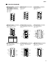
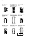
Ic block diagram dme32 19 mm74hcu04sjx (xy070a00) tc74hc04af (xs993a00) hd74lvc04fp (xw905a00) hex inverter main: pnr: mm74hc14sjx (xw104a00) hex inverter main: ic19 74vhc32sjx (xy306a00) quad 2 input or main: ic3, 5 mm74hc74asjx (xy153a00) dual d-type flip-flop main: ic17, 22 tc74hc123af (xn242a00)...
Page 20
Dme32 20 mm74hc175sjx (xy307a00) quad d-type flip-flop main: ic24, 46-49 mm74hc245asjx (xw107a00) sn74abt245bnsr (xu009a00) tc74vhc245f (xt487a00) octal 3-state bus transceiver main: ic29-31, 50-52, 60, 61, 66-75 mm74hc273sjx (xy198a00) octal d-type flir flop main: ic23 tc74hc4052af (xs790a00) diffe...
Page 21
Dme32 21 ds26c32atmx (xu815a00) quad differential line receiver main: ic32, 33, 120, 121 njm2082m-t1 (xn797a00) dual operational amplifier main: ic1 1 2 3 4 5 6 7 input a input a output a output c input c input c gnd enable 16 15 14 13 12 11 vcc input b input b output b enable output d input d 8 9 1...
Page 22: Test Program and Inspection
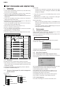
Test program and inspection dme32 22 1. Preparation 1-1. Initial settings • connect the [cascade in] terminal and [cascade out] terminal with a scsi 50p cable. • connect the [pc control] terminal and pc (windows machine) serial terminal with a d-sub 9b cross cable. • connect the [midi in] terminal a...
Page 23
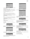
Dme32 23 click [next] and check boxes are set to on and the inspection goes to the next item. Use the following buttons as needed. Click [end] to end the test program. The screen returns to the one shown in “2-2-1 selecting the main sheet inspection items”. Click [abort] to interrupt the diagnosis. ...
Page 24
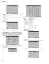
Dme32 24 (1) dsp6 displays the results of a circuit check from the so terminal of dsp6 to the si terminal of dsp6 via dsp5. (2) dram displays the results of the dram address bus and data bus connected to dsp6. 2-2-7. Dsp5 displays the results of connections for all dsp5. 2-3. Comprehensive inspectio...
Page 25
2-3-6. Switch press the switches in the sequence indicated and the results of the diagnosis will be shown. 2-3-7. Data encoder turn [data] knob in the direction indicated and the results of the diagnosis will be shown. 2-3-8. Gpi connect the gpi inspection jig to the gpi terminal indicated. (1) gpi ...
Page 26
3-3. Cascade in/out check 3-3-1. Connection • checks dme32 for one set of two units. Both dme32 should have the latest version of the firmware loaded. • connect the [cascade in] terminal for one unit with the [cascade out] terminal for the outer unit with a scsi 50p cable. • connect the [pc control]...
Page 27: Flash Rom Upgrade
Dme32 27 flash rom upgrade 1. Turn on the power with press and hold [store] and [0] keys on dme32. Lcd display on dme32. 2. Press [recall] key on dme32. Then, wait until display showing the following. 3. Transmit “dme.Bin” files. Set up port of communication soft on pc. (ex. Hyperterm) like follows....
Page 28: Error Message
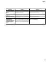
Dme32 28 if the dme32 displays an error message, look for the solution in the following table. ****** warning ****** low battery aborted-toomany errors! Application prog error! Cascade err (my id: ) cpu address error! Dma address error! Dme i/f err ext ram read/write err! Flash rom checksum err! Fla...
Page 29
Dme32 29 dme manager error messages if dme manager displays an error message, look for the solution in the following table. Cannot compile because configuration contains no components! Cannot display more than 32 meters! Com port open error 5 component position error! Configuration must be compiled ...
Page 30
Dme32 30 this operation is protected! Too many components for dme32 #! You must enter a title for the configuration! You must enter a title for the user module! Available resources are low. Further editing is not recommended. Delete some components or restart the program to resolve the problem. An a...
Page 31: Midi Implementation Chart
Dme32 31 yamaha [digital mixing engine] date: 1 may 2000 model: dme32 midi implementation chart version: 1.0 function... Transmitted recognized remarks basic channel default changed 1–16 1–16 1–16 1–16 memorized mode default messages altered x x ************** omni off/omni on x x memorized note num...
Page 32: Midi Data Format
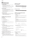
Dme32 32 midi data format 1. Transmit/receive data 1.1 program change when a program change message is received, the scene specified in the [program change assign table] is recalled. Program change messages are transmitted according to the [program change assign table]. If a scene memory number has ...
Page 33
Dme32 33 transmission i f [program change tx] is on, this message is transmitted on the [tx ch] according to the settings of the [program change assign table] when a scene is recalled. If the scene memory number that was recalled is assigned to more than one program change, the lowest-numbered progr...
Page 34: Circuit Boards
3na-v512960 2 pnr1/3(mymb) circuit board pnr3/3(gpi) circuit board pnr2/3(pcmusb) circuit board slot 1 slot 2 slot 3 slot 4 to power supply unit-cn2 to main -cn012 to power supply unit -cn4 to main -cn014 to main -cn013 to main -cn011 to main -cn017 to main -cn018 card to main-cn010 to power supply ...
Page 35: •
3na-v512930-2 2 cascade in cascade out com midi in out in out word clock to power supply unit-cn5 to pnr1/3(mymb)-cn606 75 off on pc control to pnr1/3(mymb)-cn608 to pnr1/3(mymb)-cn607 to pnr1/3(mymb)-cn605 to pnr3/3(gpi)-cn701 to pnf1/4(fp)-cn201 to pnf1/4(fp)-cn202 to pnf2/4(enc)-cn301 to pnr2/3(p...
Page 36
3na-v512930-3 1 main circuit board dme32 36 note: see parts list for details of circuit board component parts. Pattern side.
Page 37
3na-v512940 1 pnf1/4(fp) circuit board pnf2/4(enc) circuit board pnf3/4(led) circuit board pnf4/4(psw) circuit board 48khz 44.1khz lock compponent parameter protect value user define dec inc 7 8 9 4 5 6 1 2 3 store 0 recall utility emergency to main-cn006 to main-cn007 to main-cn005 to power supply ...
Page 38: Parts List
Contents overall assembly······························································································································ 2 front panel assembly ····················································································································· 5 elect...
Page 39: Overall Assembly
Dme32 2 overall assembly 470 460 450 440 400 210 350 340 190 390 360b 200 180 370 260 275 270 130 380 40 190 430 420 290 70 170 100 250 220 60 70 240 140 275 320 150 120 360a 230 230 h, w, b, v j, u 235 280 63 80 110 145 170 160 350 340 35 320 500 310 90 10 10a 10d 10b 10c 65 40c 40b 40a 40d 40ba 36...
Page 40
Dme32 3 overall assembly overall assembly overall assembly overall assembly bottom assembly bottom chassis leg bind head tapping screw-b protection sheet label label rear panel assembly rear panel assembly rear panel assembly rear panel rear panel rear panel rear panel connector assembly ac inlet su...
Page 41
Dme32 4 bonding tapping screw-b bind head tapping screw-b lithium battery top cover bind head tapping screw-b if plate bind head screw label, date cord accessories euroblock connector cable, d-sub holder, ac cord compact disc adapter, ac cord ac cord ac cord ac cord ac cord description 430 440 450 4...
Page 42: Front Panel Assembly
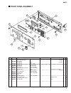
Dme32 5 front panel assembly front panel assembly sub chassis circuit board circuit board circuit board circuit board circuit board bind head tapping screw-b lcd assembly lcd pan head screw bonding screw front panel cover oval head screw power switch knob escutcheon, power switch knob, encoder descr...
Page 43: Electrical Parts
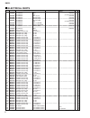
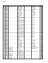
Dme32 6 electrical parts circuit board circuit board circuit board circuit board circuit board circuit board circuit board circuit board circuit board circuit board circuit board battery holder monolithic ceramic cap. Electrolytic cap. (chip) electrolytic cap. (chip) electrolytic cap. (chip) monolit...
Page 44
Dme32 7 wire trap wire trap header, flat cable connector, fcn-235d connector, ffc connector, ffc connector, fcn-235d base post connector connector, ffc connector, ffc diode diode diode diode diode diode array diode array lc filter lc filter lc filter lc filter lc filter lc filter lc filter lc filter...
Page 45
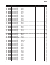
Dme32 8 ic ic ic ic ic ic ic ic ic ic ic ic ic ic ic ic ic ic ic ic ic ic ic ic ic ic ic ic ic ic ic ic ic ic ic ic ic ic ic ic ic ic ic ic ic ic ic ic ic ic ic ic ic ic ic din connector bnc connector bnc connector chip inductance chip bead core chip bead core coil coil chip inductance chip inductan...
Page 46
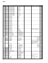
Dme32 9 led (chip) carbon resistor (chip) carbon resistor (chip) carbon resistor (chip) carbon resistor (chip) carbon resistor (chip) carbon resistor (chip) carbon resistor (chip) carbon resistor (chip) carbon resistor (chip) carbon resistor (chip) carbon resistor (chip) carbon resistor (chip) carbo...
Page 47
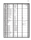
Dme32 10 carbon resistor (chip) carbon resistor (chip) carbon resistor (chip) carbon resistor (chip) carbon resistor (chip) carbon resistor (chip) carbon resistor (chip) carbon resistor (chip) carbon resistor (chip) carbon resistor (chip) carbon resistor (chip) carbon resistor (chip) carbon resistor...
Page 48
Dme32 11 circuit board circuit board circuit board circuit board bind head screw bind head screw hexagonal nut hexagonal nut shield plate electrolytic cap. (chip) electrolytic cap. (chip) monolithic ceramic cap. Monolithic ceramic cap. Monolithic ceramic cap. Monolithic ceramic cap. Monolithic ceram...
Page 49
Dme32 12 lcd assembly ac inlet lithium battery cable, d-sub ac cord ac cord ac cord ac cord description ref no. V5149400 v5065200 vn103500 v5436200 vn580000 vb506800 vb928000 v6190800 part no. 24x2 m1908-c 3p cr2032 17je 414 9p dc-015-j01 2.5m csa vde bs 3p configuration-scene ac in j u,v h,w b rema...
Page 50: Circuit Diagram
Circuit diagram warning components having special characteristics are marked and must be replaced with parts having specification equal to those originally installed. Note: see parts list for details of circuit board component parts. Digital mixing engine block diagram ······························...
Page 51
G f h d c b a e block diagram 002 (dme32) dme32 block diagram 002 (dme32) kec-92547-002 1 2 3 4 5 6 ic006 flash memory 8mbit d[0-15],a[1-19] d[0-7],a[1-17] /mrd,/wrl /mrd,/wrh d[8-15],a[1-17] /mrd,/wrl d[0-7],a[1-17] d[8-15],a[1-17] /mrd,/wrl d[0-7],a[1-17] /mrd,/wrh d[8-15],a[1-17] /mrd,/wrl p.3 ic...
Page 52
G f h d c b a 1 2 3 4 5 6 e block diagram 003 (dme32) dme32 block diagram 003 (dme32) kec-92547-003 x004 60mhz dsp5 dsp5 d51s[40-43] d51s[44-47] ic106 208p d52s[24-27] d52s[28-31] d52s[32-35] d52s[36-39] d52s[40-43] d52s[44-47] ic107 208p 17 18 mckd ssync d51s[16-19] d51s[20-23] dsp6 d51s[24-27] d51...
Page 53
B c d e f g h i j k l m n o p a 1 3 2 8 7 6 5 4 9 10 12 11 wiring (dme32) dme32 wiring (dme32) kec-92548 pnr (pcmusb) main pnf primary power supply (psw) lcd ass'y (v514940) pnf (led) pnf (enc) pnr (gpi) pnf (fp) pnr (mymb) lcd display secondary 5.
Page 54
B c d e f g h i j k l m n o p a main circuit diagram 002 (dme32) dme32 main circuit diagram 002 (dme32) kec-92549-002 6 1 3 2 8 7 6 5 4 9 10 12 11 or system reset or op amp op amp or cpu : ceramic capacitor 6.
Page 55
B c d e f g h i j k l m n o p a 1 3 2 8 7 6 5 4 9 10 12 11 main circuit diagram 003 (dme32) dme32 main circuit diagram 003 (dme32) kec-92549-003 2 flash rom 8m sram 1m sram 1m sram 1m sram 1m sram 1m sram 1m sram 1m sram 1m : ceramic capacitor 7.
Page 56
B c d e f g h i j k l m n o p a 1 3 2 8 7 6 5 4 9 10 12 11 main circuit diagram 004 (dme32) dme32 main circuit diagram 004 (dme32) kec-92549-004 6 fpga : ceramic capacitor 8.
Page 57
B c d e f g h i j k l m n o p a 1 3 2 8 7 6 5 4 9 10 12 11 main circuit diagram 005 (dme32) dme32 main circuit diagram 005 (dme32) kec-92549-005 6 d-ff inverter inverter photo coupler inverter inverter d-ff line driver /receiver : ceramic capacitor uart 9.
Page 58
B c d e f g h i j k l m n o p a 1 3 2 8 7 6 5 4 9 10 12 11 main circuit diagram 006 (dme32) dme32 main circuit diagram 006 (dme32) kec-92549-006 6 : mylar capacitor data selector data selector d-ff d-ff d-ff d-ff inverter dir2 transceiver transceiver inverter transceiver : ceramic capacitor to pnf 1...
Page 59
B c d e f g h i j k l m n o p a 1 3 2 8 7 6 5 4 9 10 12 11 main circuit diagram 007 (dme32) dme32 main circuit diagram 007 (dme32) kec-92549-007 6 line receiver line receiver line driver line driver line driver line driver /receiver : ceramic capacitor 11.
Page 60
B c d e f g h i j k l m n o p a 1 3 2 8 7 6 5 4 9 10 12 11 main circuit diagram 008 (dme32) dme32 main circuit diagram 008 (dme32) kec-92549-008 6 : mylar capacitor atsc line reciever dir2 single shot or or inverter inverter line driver atsc : ceramic capacitor 12.
Page 61
B c d e f g h i j k l m n o p a 1 3 2 8 7 6 5 4 9 10 12 11 main circuit diagram 009 (dme32) dme32 main circuit diagram 009 (dme32) kec-92549-009 6 multiplexer multiplexer d-ff transciever transciever d-ff d-ff d-ff : ceramic capacitor to pnr 3/3 (gpi)-cn701 13.
Page 62
B c d e f g h i j k l m n o p a 1 3 2 8 7 6 5 4 9 10 12 11 main circuit diagram 010 (dme32) dme32 main circuit diagram 010 (dme32) kec-92549-010 6 transciever transciever transciever transciever transciever transciever transciever transciever transciever transciever to pnr 1/3 (mymb)-cn605 to pnr 1/...
Page 63
B c d e f g h i j k l m n o p a 1 3 2 8 7 6 5 4 9 10 12 11 main circuit diagram 011 (dme32) dme32 main circuit diagram 011 (dme32) kec-92549-011 6 data selector data selector decorder decorder transciever transciever transciever transciever transciever transciever transciever transciever : ceramic c...
Page 64
B c d e f g h i j k l m n o p a 1 3 2 8 7 6 5 4 9 10 12 11 main circuit diagram 012 (dme32) dme32 main circuit diagram 012 (dme32) kec-92549-012 6 transciever transciever dsp6 dsp6 dram 16m dram 16m dram 16m dram 16m : ceramic capacitor 16.
Page 65
B c d e f g h i j k l m n o p a 1 3 2 8 7 6 5 4 9 10 12 11 main circuit diagram 013 (dme32) dme32 main circuit diagram 013 (dme32) kec-92549-013 6 dram 16m dram 16m dram 16m dram 16m dsp6 dsp6 : ceramic capacitor 17.
Page 66
B c d e f g h i j k l m n o p a 1 3 2 8 7 6 5 4 9 10 12 11 main circuit diagram 014 (dme32) dme32 main circuit diagram 014 (dme32) kec-92549-014 6 dram 16m dsp6 dsp6 dram 16m dram 16m dram 16m : ceramic capacitor 18.
Page 67
B c d e f g h i j k l m n o p a 1 3 2 8 7 6 5 4 9 10 12 11 main circuit diagram 015 (dme32) dme32 main circuit diagram 015 (dme32) kec-92549-015 6 dram 16m dram 16m dram 16m dram 16m dsp6 dsp6 : ceramic capacitor 19.
Page 68
B c d e f g h i j k l m n o p a 1 3 2 8 7 6 5 4 9 10 12 11 main circuit diagram 016 (dme32) dme32 main circuit diagram 016 (dme32) kec-92549-016 6 dram 16m dram 16m dsp6 dram 16m dram 16m dsp6 : ceramic capacitor 20
Page 69
B c d e f g h i j k l m n o p a 1 3 2 8 7 6 5 4 9 10 12 11 main circuit diagram 017 (dme32) dme32 main circuit diagram 017 (dme32) kec-92549-017 6 dsp5 dsp5 multiplexer multiplexer : ceramic capacitor 21.
Page 70
B c d e f g h i j k l m n o p a 1 3 2 8 7 6 5 4 9 10 12 11 main circuit diagram 018 (dme32) dme32 main circuit diagram 018 (dme32) kec-92549-018 6 dsp5 : ceramic capacitor 22.
Page 71
B c d e f g h i j k l m n o p a 1 3 2 8 7 6 5 4 9 10 12 11 main circuit diagram 019 (dme32) dme32 main circuit diagram 019 (dme32) kec-92549-019 6 transciever transciever transciever transciever transciever transciever transciever from power supply unit - cn5 to pnr 2/3 (pcmusb) - cn101 to pnr 2/3 (...
Page 72
B c d e f g h i j k l m n o p a 1 3 2 8 7 6 5 4 9 10 12 11 main circuit diagram 020 (dme32) dme32 main circuit diagram 020 (dme32) kec-92549-020 6 line driver line driver line reciever line reciever line reciever/driver : ceramic capacitor 24.
Page 73
G f h d c b a e pnf circuit diagram (dme32) dme32 pnf circuit diagram (dme32) kec-92550 1 2 3 4 5 6 to main-cn006 to main-cn004 to main-cn005 to main-cn007 to power supply unit - cn1 to ac inlet pnf 3/4 led pnf 1/4 fp pnf 2/4 enc pnf 4/4 psw 25.
Page 74
B c d e f g h i j k l m n o p a 1 3 2 8 7 6 5 4 9 10 12 11 dme32 pnr 2/3 (pcmusb) circuit diagram 002 (dme32) kec-92551-002 1 pnr 2/3 (pcmusb) circuit diagram 002 (dme32) power connector power controller pc card controller usb i/f inverter to main-cn017 to main-cn018 to power supply unit -cn4 : cera...
Page 75
B c d e f g h i j k l m n o p a 1 3 2 8 7 6 5 4 9 10 12 11 pnr 1/3 (mymb) circuit diagram 003 (dme32) dme32 pnr 1/3 (mymb) circuit diagram 003 (dme32) kec-92551-003 to main-cn012 to main-cn014 to main-cn013 to main-cn011 to power supply unit-cn2 27.
Page 76
G f h d c b a 1 2 3 4 5 6 e pnr 3/3 (gpi) circuit diagram 004 (dme32) dme32 pnr 3/3 (gpi) circuit diagram 004 (dme32) kec-92551-004 2 to main-cn010 to power supply unit-cn3 in/+v slot 1-8 in/+v slot 9-16 out/gnd slot 9-16 out/gnd slot 1-8 28.
Page 77
B c d e f g h i j k l m n o p a 1 3 2 8 7 6 5 4 9 10 12 11 power supply unit circuit diagram 1/3 (dme32) dme32 power supply unit circuit diagram 1/3 (dme32) v484590 ic1 nba-0448-o-1 r26 150k/f c16 0.1/50 c11 100/25 d10 0 d11 1ss133 c66 27/35 d3 1gwj43 c2 0.1/250 r18 47 d1 d3sba60 ic3 fa5332p 9 10 11...
Page 78
B c d e f g h i j k l m n o p a 1 3 2 8 7 6 5 4 9 10 12 11 power supply unit circuit diagram 2/3 (dme32) dme32 power supply unit circuit diagram 2/3 (dme32) v484590 to pnr 1/3 (mymb) -cn609 to pnr 3/3 (gpi) -cn702 to pnr 2/3 (pcmusb) -cn103 to main -cn16 +5v gnd(+5v) +3.3v gnd(+3.3v) gnd(+3.3v) gnd(...
Page 79
B c d e f g h i j k l m n o p a 1 3 2 8 7 6 5 4 9 10 12 11 power supply unit circuit diagram 3/3 (dme32) dme32 power supply unit circuit diagram 3/3 (dme32) q101 2sd1863r r109 10k/f r111 33k/f c106 2200p/50 r112 220k r113 2.2k/f t101 nt-358 6 5 3 4 1 2 c104 100p/50 d104 1ss133 q102 2sb1241r c101 100...

